2 layers

 dteal/hvawg
High voltage modular arbitrary waveform generator.
Hvawg is an open-source printed circuit board by dteal, from the dteal/hvawg repository on GitHub. It is a 2-layer board of 150 × 40 mm with 90 parts on 50 nets, routed with 595 tracks and 43 vias.
It is built around the LM8261M5, NE5532 and L7805, with the IRF730 and IRF9610PBF among its other parts. Its parts include 27 capacitors, 21 resistors, 10 connectors, 7 ICs and 3 diodes.


This is the first draft iteration of a modular arbitrary waveform generator intended to generate possibly tens of separate ±100V 1MHz signals for small capacitive loads, e.g., electrostatic actuators or ion traps.
WARNING: THIS BOARD IS DANGEROUS. IT USES SOMEWHAT HIGH VOLTAGES AT SOMEWHAT HIGH POWER. DO NOT BUILD, TEST, OR USE WITHOUT BOTH CAUTION AND KNOWING WHAT YOU ARE DOING. No guarantees or warranty or support is provided, etc.
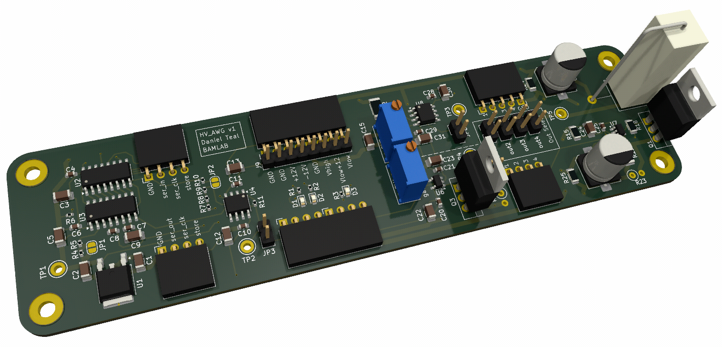
Specifications:
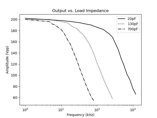
Measured frequency response:
(generated by feeding external signal into on-board amplifier bypassing DAC)
This circuit was made with the following constraints in mind:
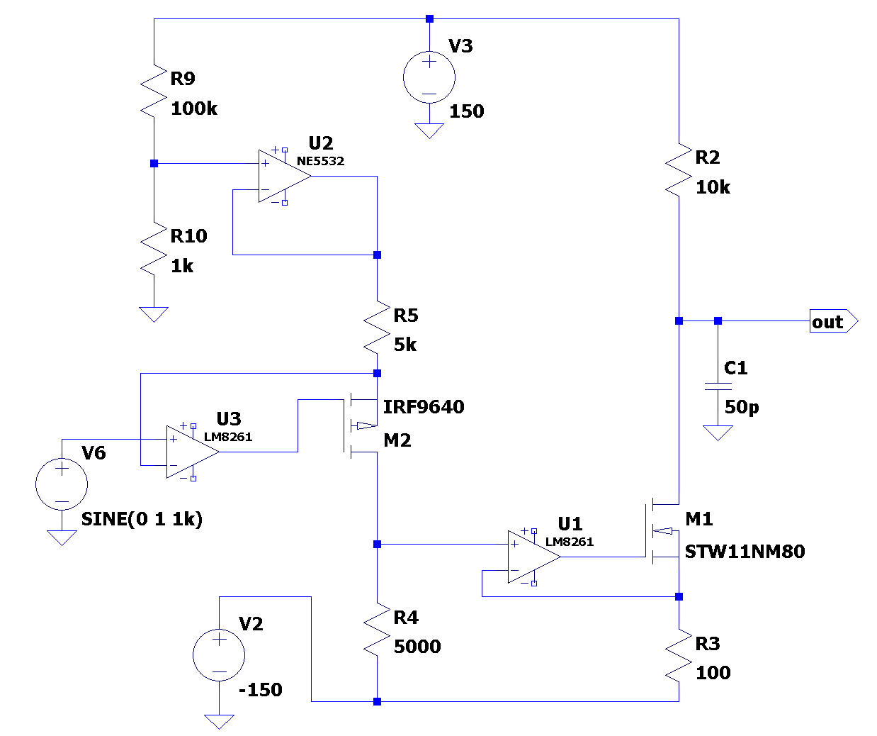
The amplifier looks something like the following:
Previous but insufficient approaches to similar problems include:
This board takes five power inputs (in addition to the GND connection, of course):
These should be turned on in the following order:
LEDs indicate when the three 12V power supplies are on.
The power supplies used for testing were Wanptek WPS series supplies (160V 2A and 30V 10A) from eBay.
The +/-100V high voltage supplies are used to drive the output and need to be capable of the full board power draw (potentially 10W each, depending on component selection and voltage output).
The +/-12V supplies are used to drive the DAC and intermediate amplifier opamps. These are not generated from the +/-100V because a linear regulator would be too lossy and a buck regulator would make the board significantly more complex and expensive. Likewise, the low 12V supply is used to drive the output amplifier opamp, and is not generated from the other supplies for the same efficiency reason.
If more convenience is required, an external board can generate the 12V and 100V supplies however desired.
The DAC circuit takes a serial input via the 74HC595 shift register and sends the output to a DAC0909 DAC chip.
The DAC is 8 bits. Four PCBs can be daisy-chained together (requiring 32 bits).
The DAC should theoretically operate up to about 100MHz, allowing four 8-bit daisy-chained boards to be updated at above 1MHz. This upper speed has not been tested yet and may be limited by inferior PCB routing.
The DAC protocol works (via the 74HC595) as follows:
This should work with any 74HC595 code, e.g., many Arduino libraries.
The level shifter circuit accepts an input +/-1V analog signal, translates this into a current, and sends the result to the negative high voltage rail, where it is converted back into an analog voltage to drive the output opamp.
The level shifter can be disconnected from the DAC via jumper JP3 in order to input an external analog signal (e.g., from a low-voltage waveform generator) for testing purposes.
Potentiometer RV1 controls the gain of the high voltage output and should be adjusted to give a 100x amplification.
NOTE: THE CURRENT PCB HAS AN ERROR (see "Errata" below) where the source and drain of PMOS transistor Q3 are switched. If this is not fixed during assembly, when the high voltage low rail is turned on, significant current will flow through R17, which will burn out due to excessive power draw.
This subcircuit provides compensation such that the final high-voltage output is independent of the high voltage supply level (i.e., high voltage inputs of +50V, +100V, and +150V should not affect a 50Vpp output signal).
Potentiometer RV2 controls the DC bias of the output and should be adjusted to center the output at GND = 0V.
Resistor R12=110kohm dissipating up to 200mW was specifically chosen to minimize power draw while also maximizing the voltage/current at the input to opamp U8A (which has nonzero input offset current).
This circuit takes an input voltage signal near the negative rail (from the level shifter) and converts this into a current signal through Q1 and R21, which form a class-A amplifier to generate the final high-voltage output. The output voltage is determined by the voltage drop of R21 with the given current.
R21 and Q1, as a class-A amplifier, form a resistive divider between the high voltage power rails, and dissipate a large (10W) current even in their quiescent state in order to drive loads with reasonable accuracy. This means they generate significant heat.
R21 was chosen at 10k as a reasonable compromise between quiescent power draw and load drive ability. R21 can be replaced with a 5kohm power resistor to draw more current but double the output load capacity.
The final output from R21 and Q1 can be connected to any one of outputs 1 through 4 via jumpers JP8 through JP11.
Four daisy-chained boards can thus be attached to separate outputs.
All SMD parts are from JLCPCB and specifically chosen from parts with reliable high stock.
Hand-soldered components were added manually afterward (not through JLCPCB) to reduce order lead time.
These boards were designed in KiCad and ordered from JLCPCB with help from the excellent kicad-jlc-pcb tools plugin https://github.com/bouni/kicad-jlcpcb-tools.
Hand assembly of the through hole components takes about 20 minutes per board.
Be sure to bend the legs of the PMOS MOSFET to switch its source and drain to fix a board error (see "Errata" section below).
Header pins are ordered in lenths of 18 to reduce costs. These should be manually cut to size (or ordered in the right size to begin with).
The power resistor R21 needs spare wires soldered on to fit the PCB footprint. The resistor hangs off the edge of the board so it can be bolted to a heatsink. It's possible these spare wires increase EMI emissions. Future board iterations could switch to a TO-220 package power resistor, matching NMOS transistor Q1, which is also at the edge of the board for easy heatsink mounting.
After the board is assembled, the following bringup/test strategy seems to work well:
| Part no. | QTY | Cost | Note | URL |
|---|---|---|---|---|
| 3296Y-1-472LF | 2 | $1.3 | 4.7kohm trimpot | https://www.digikey.com/en/products/detail/bourns-inc/3296Y-1-472LF/2536016 |
| IRF9610PBF | 1 | $1.1 | PMOS power FET | https://www.digikey.com/en/products/detail/vishay-siliconix/IRF9610PBF/811768 |
| IRF730PBF | 1 | $1.1 | NMOS power FET | https://www.digikey.com/en/products/detail/vishay-siliconix/IRF730PBF/811793 |
| QPC02SXGN-RC | 4 | $0.04 | jumper | https://www.digikey.com/en/products/detail/sullins-connector-solutions/QPC02SXGN-RC/2618262 |
| THS2510KJ | 1 | $2.5 | 10kohm power resistor | https://www.digikey.com/en/products/detail/te-connectivity-passive-product/THS2510KJ/2366983 |
| PREC018SABN-RC | 3 | $0.25 | 18-pin male header | https://www.digikey.com/en/products/detail/sullins-connector-solutions/PREC018SABN-RC/2775036 |
| PPPC181LGBN-RC | 3 | $0.82 | 18-pin female header | https://www.digikey.com/en/products/detail/sullins-connector-solutions/PPPC181LGBN-RC/775951 |
Board error:
EMI issue:
Improvements:
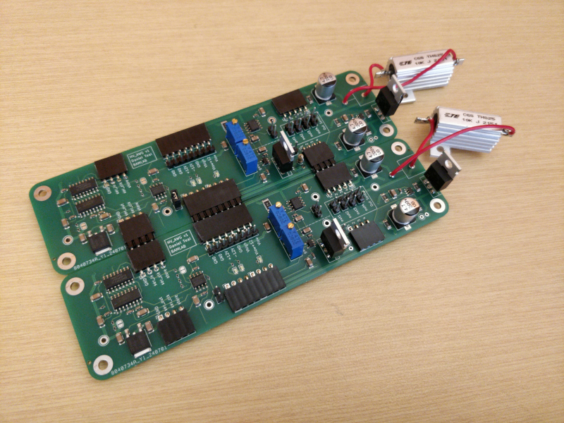
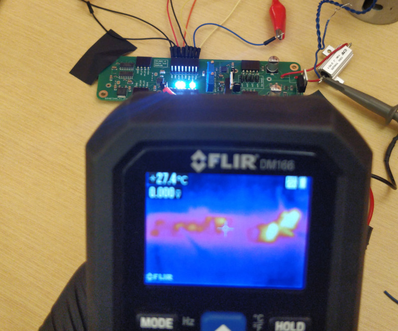
Note the hottest parts of the circuit are the power resistor and MOSFET near the output, as expected.
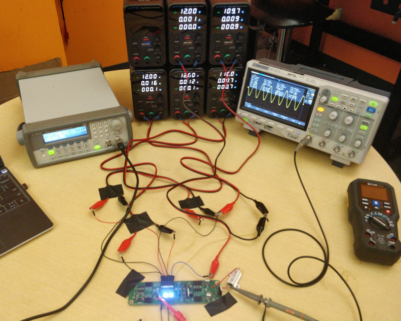
An external function generator was used to generate test waveforms by disconnecting the DAC via jumper JP3.
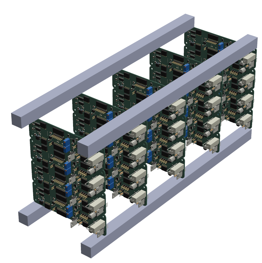
Heatsinks, external wires, and control board not included. Note a large flat heatsink is easy to add along the output power resistors and MOSFETs.
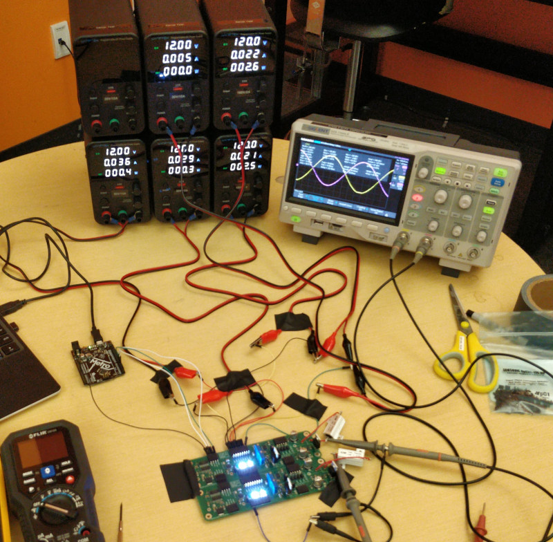
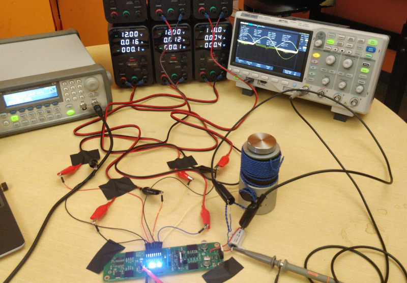
Several-foot-long unshielded wires connected to the output and a capacitive load interfere with the signal generator. Note the waveform on the oscilloscope only shows half a sinusoid; the lower half was somehow blocked. The test was immediately stopped.
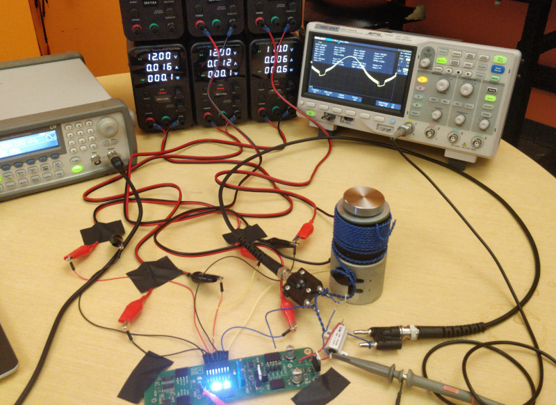
Using a shielded cable reduced interference, but that's still not a perfect sinusoid on the oscilloscope. Recommendation: improve PCB to minimize external wires and other possible EMI sources and use a proper RF SMA connector for the output.
| Qty | Value | Footprint | References |
|---|---|---|---|
| 13 | 10u | Capacitor_SMD:C_1206_3216Metric | C1, C2, C3, C5, C9, C12, C13, C15, C22, C23, C24, C30, C31 |
| 12 | 100n | Capacitor_SMD:C_0603_1608Metric | C4, C6, C7, C8, C10, C11, C14, C20, C21, C25, C28, C29 |
| 12 | 2.7k | Resistor_SMD:R_0402_1005Metric | R1, R2, R3, R4, R5, R6, R7, R8, R9, R10, R11, R17 |
| 5 | TestPoint | TestPoint:TestPoint_Keystone_5005-5009_Compact | TP1, TP2, TP3, TP4, TP5 |
| 4 | 1M | Resistor_SMD:R_1206_3216Metric | R15, R18, R24, R25 |
| 4 | Conn_01x04_Pin | Library:PinSocket_1x04_P2.54mm_Horizontal_flipped | J1, J3, J5, J7 |
| 4 | Conn_01x04_Pin | Connector_PinSocket_2.54mm:PinSocket_1x04_P2.54mm_Horizontal | J2, J4, J6, J8 |
| 4 | Jumper_2_Open | Connector_PinHeader_2.54mm:PinHeader_1x02_P2.54mm_Vertical | JP8, JP9, JP10, JP11 |
| 4 | MountingHole | MountingHole:MountingHole_3.2mm_M3_Pad | H1, H2, H3, H4 |
| 3 | Jumper_2_Bridged | Connector_PinHeader_2.54mm:PinHeader_1x02_P2.54mm_Vertical | JP3, JP4, JP6 |
| 3 | LED | LED_SMD:LED_0603_1608Metric | D1, D2, D3 |
| 2 | 100 | Resistor_THT:R_Axial_DIN0207_L6.3mm_D2.5mm_P2.54mm_Vertical | R19, R23 |
| 2 | 4.7u | Capacitor_SMD:CP_Elec_8x10.5 | C26, C27 |
| 2 | LM8261 | Package_TO_SOT_SMD:SOT-23-5 | U6, U7 |
| 2 | NE5532 | Package_SO:SOIC-8_3.9x4.9mm_P1.27mm | U4, U8 |
| 1 | 10k | Resistor_THT:R_Axial_Power_L25.0mm_W9.0mm_P10.16mm_Vertical | R21 |
| 1 | 110k | Resistor_SMD:R_2010_5025Metric | R12 |
| 1 | 1k | Potentiometer_THT:Potentiometer_Bourns_3296Y_Vertical | RV2 |
| 1 | 3k | Potentiometer_THT:Potentiometer_Bourns_3296Y_Vertical | RV1 |
| 1 | 74HC595D,110 | Package_SO:SOIC-16_3.9x9.9mm_P1.27mm | U2 |
| 1 | 75 | Resistor_SMD:R_2010_5025Metric | R22 |
| 1 | Conn_01x01_Pin | Connector_PinSocket_2.54mm:PinSocket_1x01_P2.54mm_Horizontal | J10 |
| 1 | Conn_01x08_Pin | Connector_PinHeader_2.54mm:PinHeader_1x08_P2.54mm_Vertical | J9 |
| 1 | DAC0808LCMX/NOPB | Package_SO:SOIC-16_3.9x9.9mm_P1.27mm | U3 |
| 1 | IRF730 | Package_TO_SOT_THT:TO-220-3_Vertical | Q1 |
| 1 | IRF9610 | Package_TO_SOT_THT:TO-220-3_Vertical | Q3 |
| 1 | L7805 | Package_TO_SOT_SMD:TO-252-2 | U1 |
| 1 | SolderJumper_2_Bridged | Jumper:SolderJumper-2_P1.3mm_Bridged_RoundedPad1.0x1.5mm | JP2 |
| 1 | SolderJumper_2_Open | Jumper:SolderJumper-2_P1.3mm_Open_RoundedPad1.0x1.5mm | JP1 |
It measures 150 × 40 mm and has 2 copper layers, 1.6 mm thick.
90 parts, built around the LM8261M5, NE5532, L7805 and IRF730. The full list of its parts is on this page, with links to each part's symbol and footprint where PCBKit's library has them.
From the dteal/hvawg repository on GitHub, at the commit this page was made from: the board is hvawg.kicad_pcb and its schematic hvawg.kicad_sch. PCBKit opens the board in the browser, with nothing to install.
Its repository states no licence, so its author keeps all rights: ask dteal before reusing the design.


stefaweb/Q17-Amplifier
The Q17 is an error correction HIFI amplifier based on the QUAD405 current dumping principle.


