

2 layers151.3 × 50.8 mm

 dslmande/TR-808PSU2
UNTESTED KiCad rebuild of the Roland TR-808 power supply board PS3116 in two versions: 230 V (PS3116-054) and 110 V (PS3116-051). Not manufactured, not safety-tested.
TR-808PSU Rev0.5-110V is an open-source printed circuit board by dslmande, from the dslmande/TR-808PSU repository on GitHub, published under the CERN-OHL-W-2.0 licence. It is a 2-layer board of 142.9 × 119.4 mm with 65 parts on 35 nets, routed with 266 tracks and 5 vias.
It is built around the W04 and 2SD880. Its parts include 16 capacitors, 13 connectors, 7 resistors, 4 diodes and 4 crystals. It belongs with the power boards of this library.
⚠️ UNTESTED
This board has not been manufactured, assembled or tested. It has not been checked against the real unit, and it has not been tested against any safety standard. The design is a copy of a historical (1984–86) circuit board. It is connected to mains voltage (230 V, or 110 V for the second variant), which can kill. Use at your own risk, and only if you know what you are doing. Dimensions are derived from a scan (±3 %), see VERIFICATION.md.
KiCad rebuild of the power supply board PS3116 (PCB 291-405A) of the Roland TR-808: schematic redrawn from the 1981 service manual, board with outline, holes, terminals and component positions taken from the original component layout. Two variants of the same board:
| Variant | Original board | Mains | Transformer | Files |
|---|---|---|---|---|
| 230 V | PS3116-054 | 220/240 V | N-219D | TR-808PSU_Rev0.5* |
| 110 V | PS3116-051 | 100/117 V (built for 110 V, 117 V tap) | N-218C | TR-808PSU_Rev0.5-110V* |
Both use the same copper; they differ in parts (fuses, transformer, switch, C1) and in the
silkscreen mark (PS3116-054 230V / PS3116-051 110V), so the boards cannot be mixed up.
Current version: Rev0.5.
| Version | Contents |
|---|---|
| Rev0.1 | historical 1:1 copy of the 1984–86 original; switched mains conductors SW_A/SW_B 3.75 mm apart |
| Rev0.2 | as Rev0.1, but SW_B moved away on the mains side: SW_A/SW_B at least 5.67 mm apart |
| Rev0.3 | as Rev0.2, but the 230 V primary side (terminals 1–9: mains, switch, transformer input) uses RM5.0 screw terminals (Phoenix MKDS 1,5) instead of solder lugs; terminals 10–22 (low voltage) stay solder lugs |
| Rev0.4 / Rev0.4-110V | as Rev0.3, but all board corners rounded to R5 (house rule), voltage mark on the silkscreen; the 110 V variant is new (fuses 0.5 A, transformer N-218C) |
| Rev0.5 / Rev0.5-110V (current) | as Rev0.4, but the voltage mark moved to the free area below the fuse holders (it touched the F4 outline). Two releases: 230 V and 110 V |
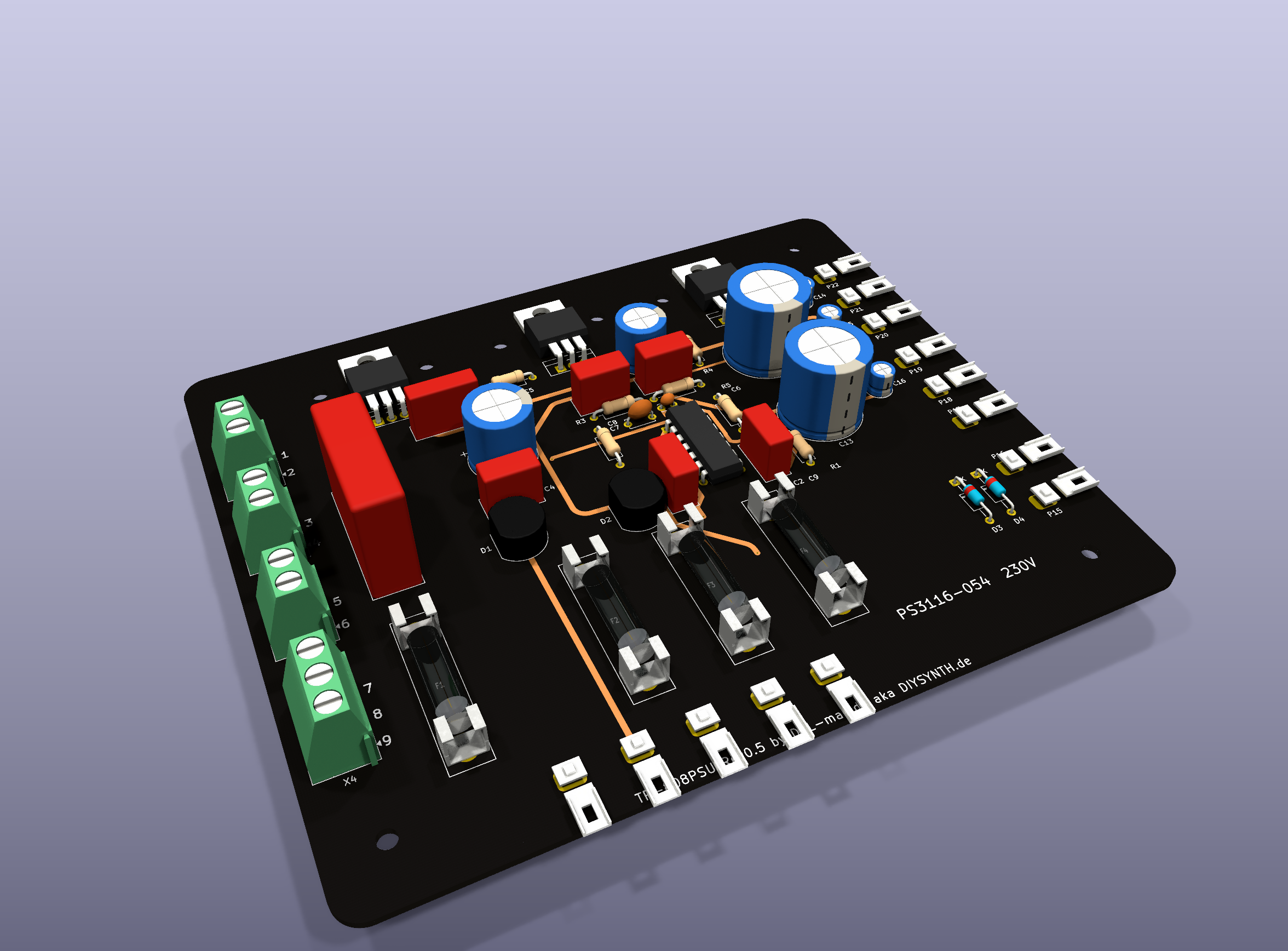
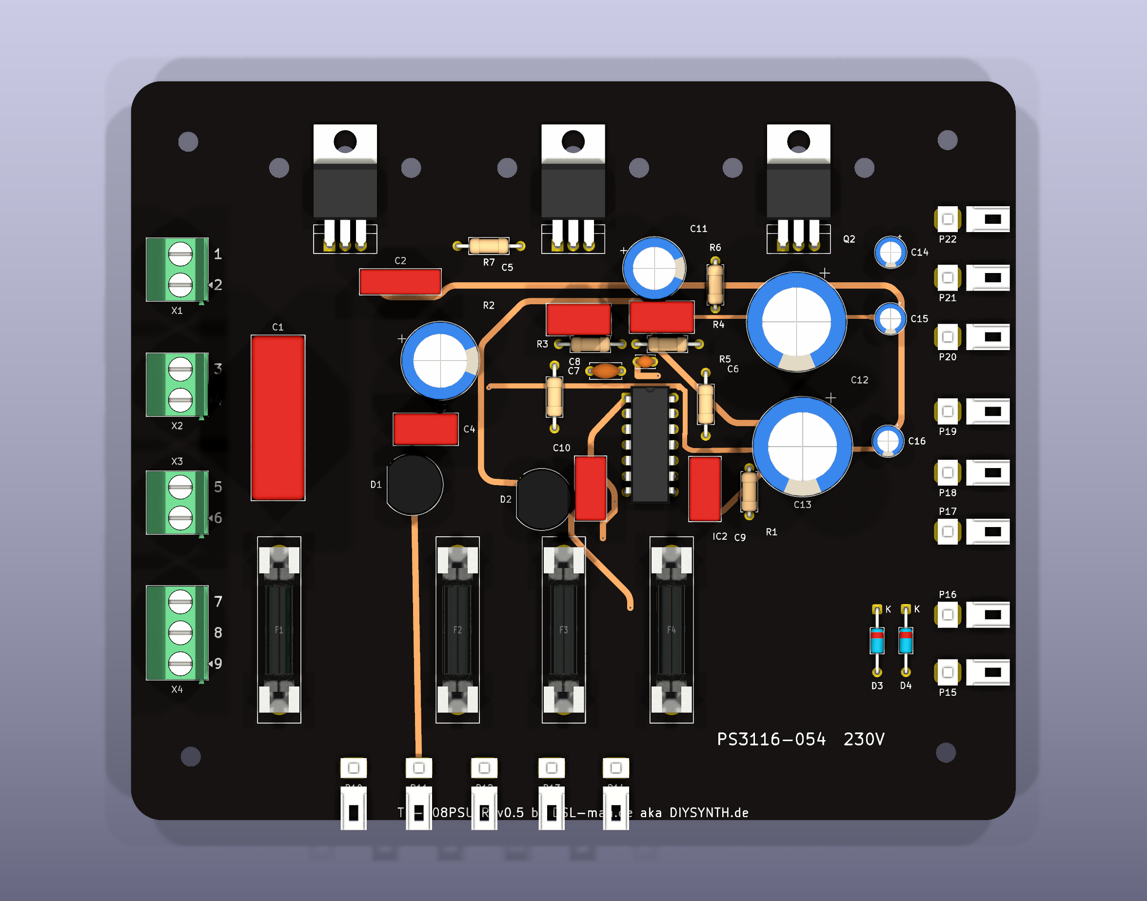
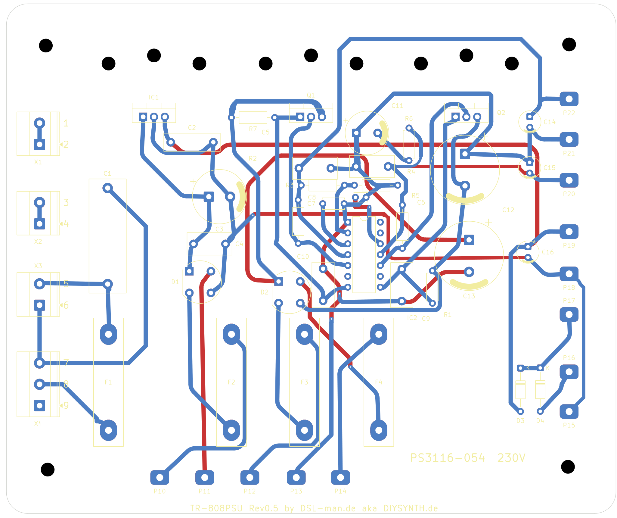
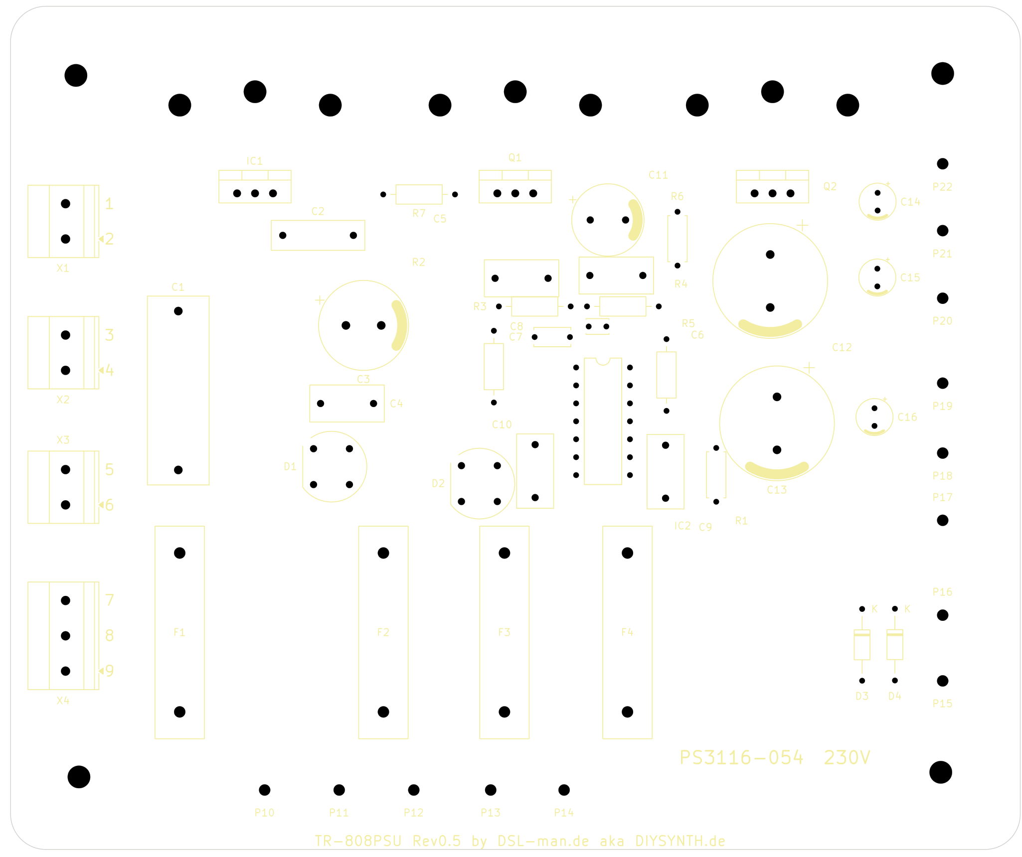
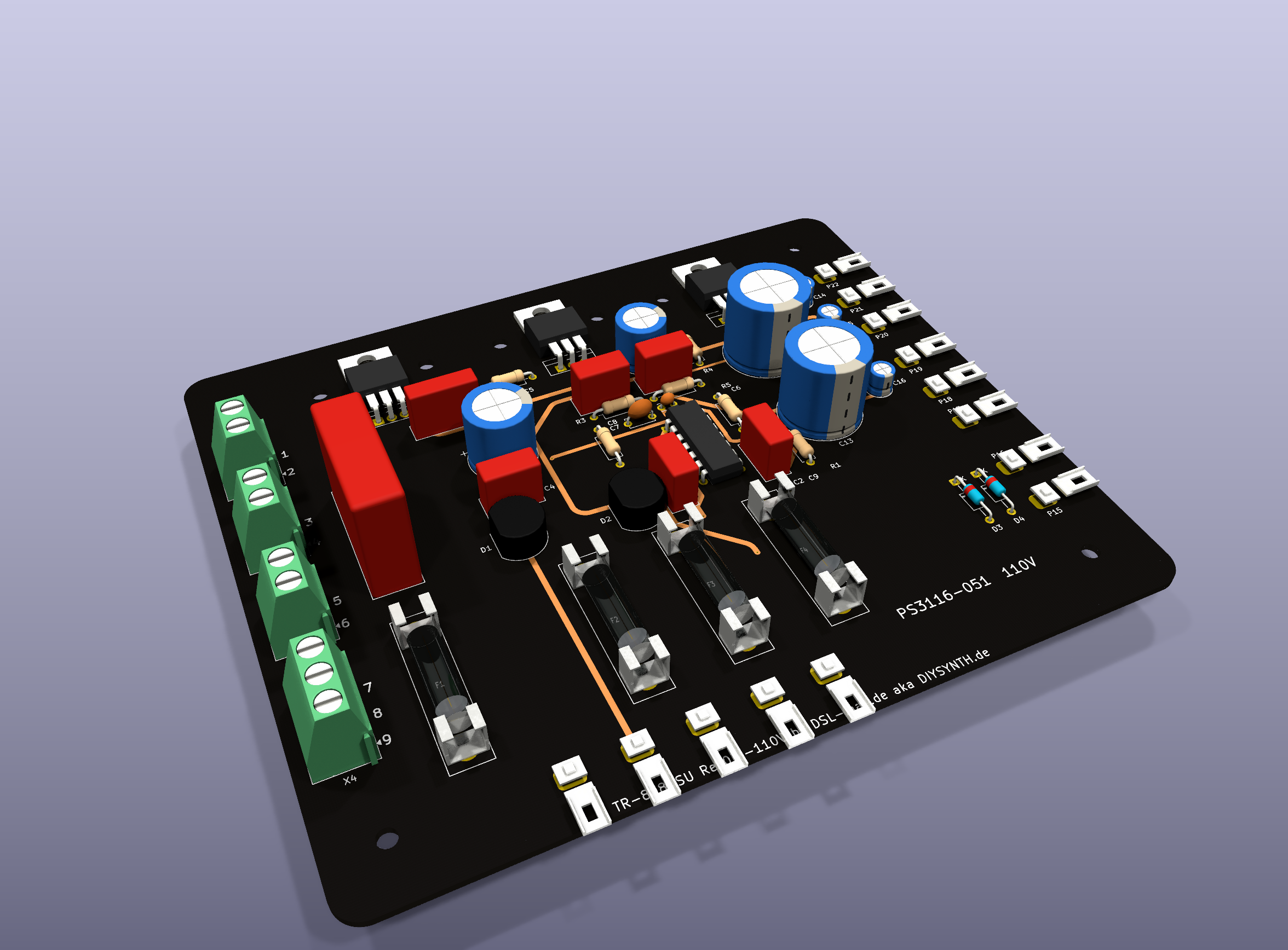
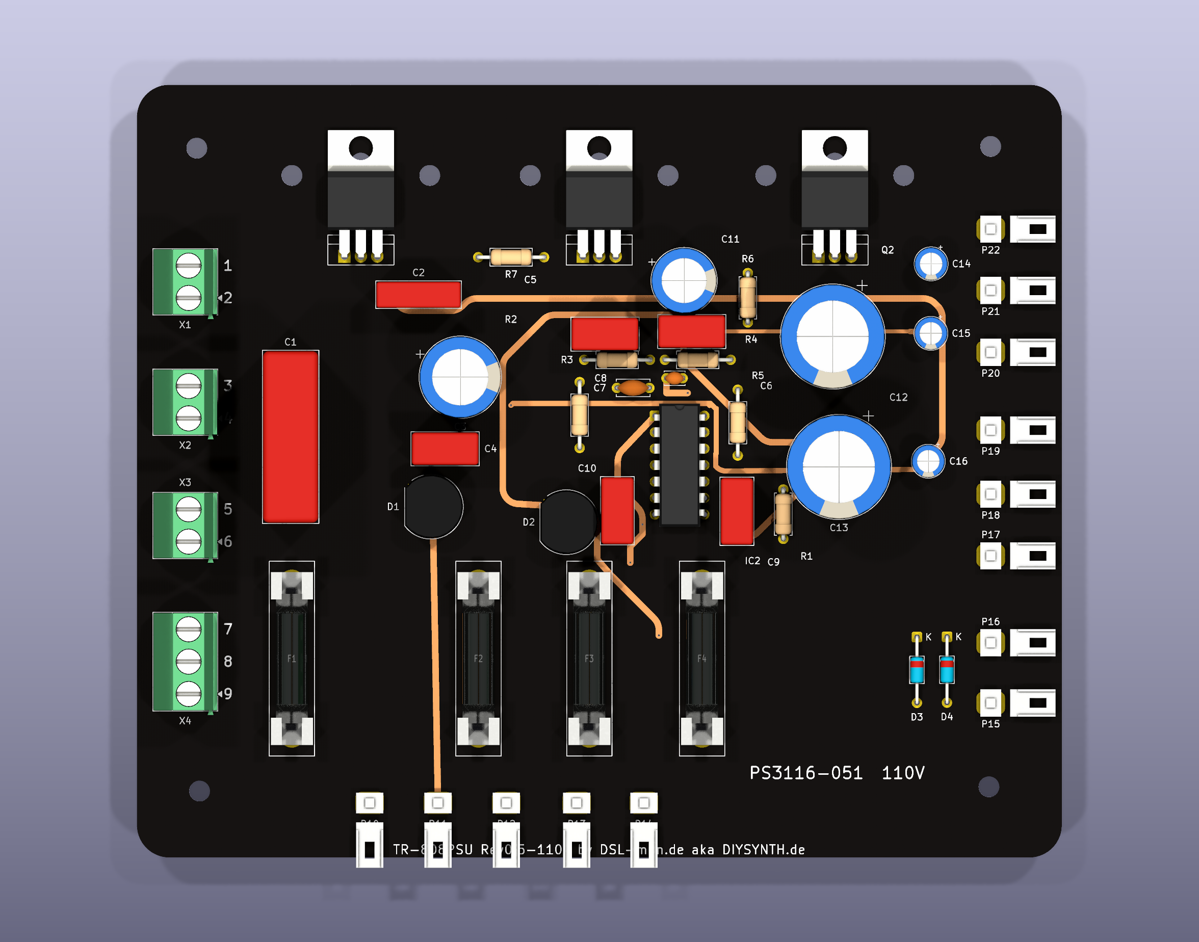
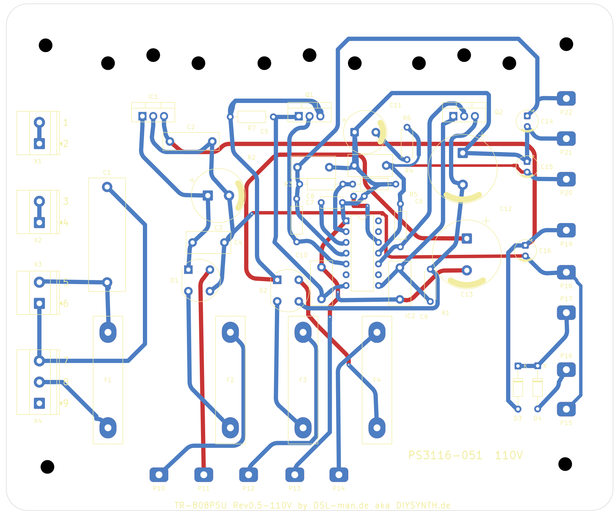
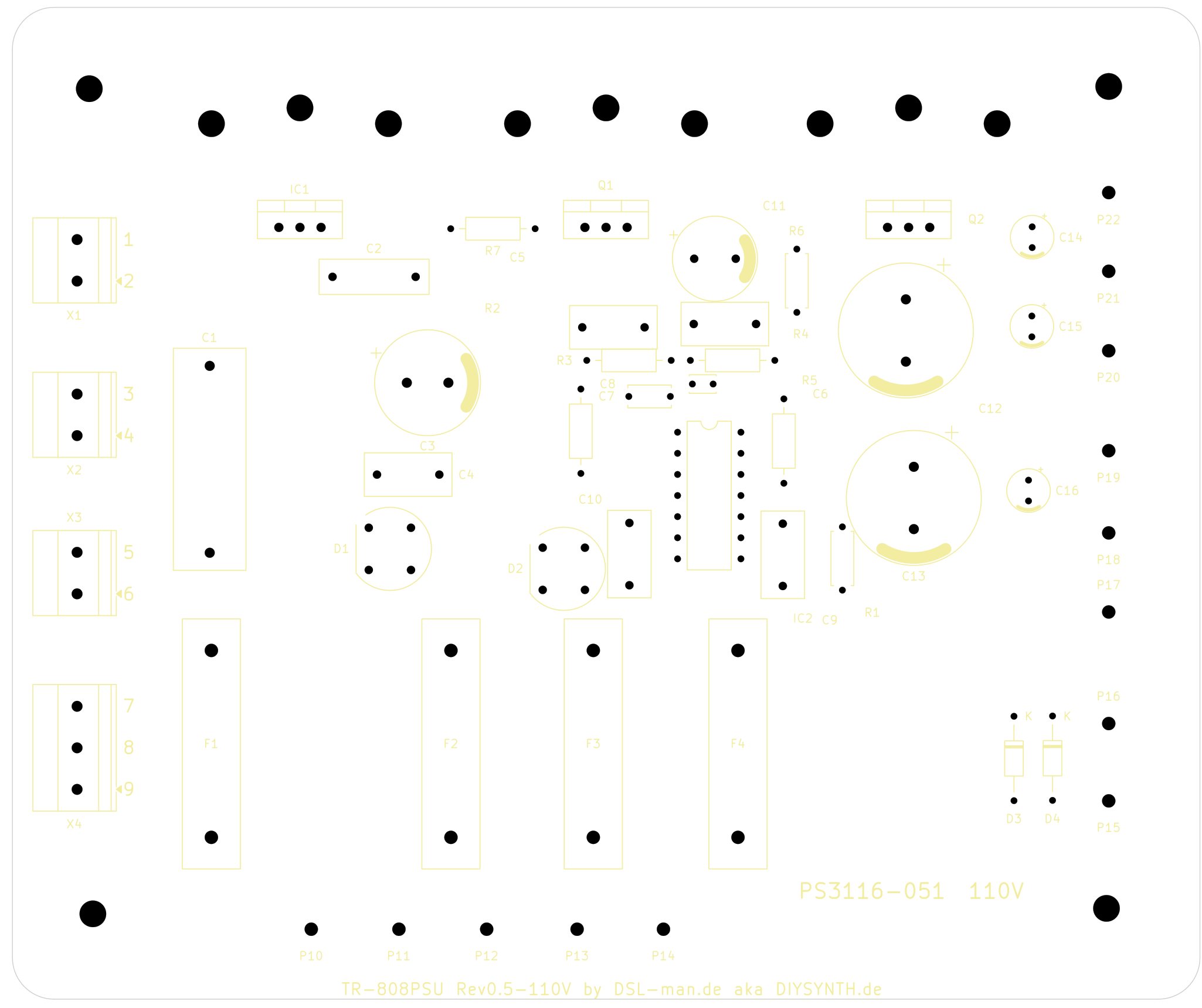
More (230 V; for 110 V use the Rev0.5-110V files, BOM-110V.md): schematic (PDF) · bill of materials (CSV) · 1:1 printout (A4) · Gerber (zip) · assembly drawing (PDF) · original copper vs. tracks · verification · releases
| File | Contents |
|---|---|
| ORIGINAL.md | source, manual pages, variants, circuit description, open points |
| VERIFICATION.md | standards context (DIN EN IEC 62368-1, IEC 60664-1), verification, validation, findings, risks |
BOM.md / BOM-110V.md, psu/TR-808PSU_Rev0.5_bom.csv | bill of materials (readable, with function and original parts; CSV) |
psu/TR-808PSU_Rev0.5.kicad_pro / .kicad_sch / .kicad_pcb (and …Rev0.5-110V…) | KiCad project |
psu/TR-808PSU_Rev0.5_schaltplan.pdf | schematic plot |
psu/gerber_TR-808PSU_Rev0.5/, psu/TR-808PSU_Rev0.5_gerber.zip | Gerber, drill data, position file |
psu/TR-808PSU_Rev0.5_ausdruck_1zu1.pdf | 1:1 printout on A4 landscape: component side, solder side, drill template (print at 100 %, check the measuring bar) |
psu/TR-808PSU_Rev0.5_3d_oben.png, _3d_schraeg.png | 3D views (KiCad ray tracing; own models for fuse holders and terminal lugs) |
psu/TR-808PSU_Rev0.5_pcb_top.pdf, _pcb_bottom.pdf, _assembly.pdf | board plots |
psu/placement.json, psu/placement_scan.json | component positions from the component layout, resp. aligned to the scan (mm) |
psu/kupfer.npz, psu/leitkarte.npz | copper mask and net regions of the original (from the scan) |
psu/TR-808PSU_Rev0.5_ueberlagerung.png | original copper against the tracks of this board |
File names with schaltplan, ausdruck, kupfer and leitkarte are German for schematic, printout, copper and guide map.
psu/TR-808PSU_Rev0.5_ueberlagerung.png shows the original copper (grey) and the tracks
(red solder side, blue component side). Pure tracing without the router fails because of
the scan quality (shorts between neighbouring tracks, pad positions only within ±0.3 mm).psu/TR-808PSU_Rev0.5-erc.rpt).Schematic and layout were generated with a private tool chain that is not part of this
repo. The KiCad project in psu/ is complete and needs only KiCad 9/10.
Hardware files (KiCad project, Gerber, schematic, documents): CERN-OHL-W-2.0 (CERN Open Hardware Licence v2, weakly reciprocal). The licence covers only this redrawing and layout, not Roland's original design or manual. Provided as is, without warranty: see the disclaimer in the licence and the UNTESTED notice above.
Circuit and dimensions come from the Roland TR-808 service manual (15 June 1981). The manual itself and the data sheets are not part of this repo (copyright of Roland and the manufacturers). This repo contains an own redrawing for repair and rebuild. "Roland" and "TR-808" are trademarks of Roland Corporation; this project is not affiliated with Roland.
Data sheets used to check the pin assignments: 2SB596 (MOSPEC), 2SD880 (DC Components), TA7179P and µA7805 (service manual, page 2).
| Qty | Value | Footprint | References |
|---|---|---|---|
| 13 | M3 | MountingHole:MountingHole_3.2mm_M3 | H1, H2, H3, H4, H5, H6, H7, H8, H9, H10, H11, H12, H13 |
| 5 | 0.1u | Capacitor_THT:C_Rect_L10.3mm_W5.0mm_P7.50mm_MKS4 | C4, C5, C6, C9, C10 |
| 4 | 0.5A | TR808PSU:FuseClip_5x20_TF785 | F1, F2, F3, F4 |
| 3 | 10u/16V | Capacitor_THT:CP_Radial_D5.0mm_P2.50mm | C14, C15, C16 |
| 3 | 2P RM5 | TerminalBlock_Phoenix:TerminalBlock_Phoenix_MKDS-1,5-2_1x02_P5.00mm_Horizontal | X1, X2, X3 |
| 2 | 1000u/35V | Capacitor_THT:CP_Radial_D16.0mm_P7.50mm | C12, C13 |
| 2 | 15k | Resistor_THT:R_Axial_DIN0207_L6.3mm_D2.5mm_P10.16mm_Horizontal | R3, R4 |
| 2 | 1S2473 | Diode_THT:D_DO-35_SOD27_P10.16mm_Horizontal | D3, D4 |
| 2 | 3.3 | Resistor_THT:R_Axial_DIN0207_L6.3mm_D2.5mm_P10.16mm_Horizontal | R2, R5 |
| 2 | W04 | Diode_THT:Diode_Bridge_Round_D9.8mm | D1, D2 |
| 1 | 0.01u | Capacitor_THT:C_Disc_D5.0mm_W2.5mm_P5.00mm | C7 |
| 1 | 0.01u | Capacitor_THT:C_Disc_D3.0mm_W2.0mm_P2.50mm | C8 |
| 1 | 0.047u/X2 | Capacitor_THT:C_Rect_L26.5mm_W8.5mm_P22.50mm_MKS4 | C1 |
| 1 | 0.1u | Capacitor_THT:C_Rect_L13.0mm_W4.0mm_P10.00mm_FKS3_FKP3_MKS4 | C2 |
| 1 | 10 | TR808PSU:Terminal_Pin | P10 |
| 1 | 1000u/16V | Capacitor_THT:CP_Radial_D12.5mm_P5.00mm | C3 |
| 1 | 11 | TR808PSU:Terminal_Pin | P11 |
| 1 | 12 | TR808PSU:Terminal_Pin | P12 |
| 1 | 13 | TR808PSU:Terminal_Pin | P13 |
| 1 | 14 | TR808PSU:Terminal_Pin | P14 |
| 1 | 15 | TR808PSU:Terminal_Pin | P15 |
| 1 | 16 | TR808PSU:Terminal_Pin | P16 |
| 1 | 17 | TR808PSU:Terminal_Pin | P17 |
| 1 | 18 | TR808PSU:Terminal_Pin | P18 |
| 1 | 19 | TR808PSU:Terminal_Pin | P19 |
| 1 | 20 | TR808PSU:Terminal_Pin | P20 |
| 1 | 21 | TR808PSU:Terminal_Pin | P21 |
| 1 | 22 | TR808PSU:Terminal_Pin | P22 |
| 1 | 220 | Resistor_THT:R_Axial_DIN0207_L6.3mm_D2.5mm_P7.62mm_Horizontal | R6 |
| 1 | 2SB596 | Package_TO_SOT_THT:TO-220-3_Vertical | Q1 |
| 1 | 2SD880 | Package_TO_SOT_THT:TO-220-3_Vertical | Q2 |
| 1 | 3P RM5 | TerminalBlock_Phoenix:TerminalBlock_Phoenix_MKDS-1,5-3_1x03_P5.00mm_Horizontal | X4 |
| 1 | 47 | Resistor_THT:R_Axial_DIN0207_L6.3mm_D2.5mm_P10.16mm_Horizontal | R7 |
| 1 | 47 | Resistor_THT:R_Axial_DIN0207_L6.3mm_D2.5mm_P7.62mm_Horizontal | R1 |
| 1 | 470u/16V | Capacitor_THT:CP_Radial_D10.0mm_P5.00mm | C11 |
| 1 | TA7179P | Package_DIP:DIP-14_W7.62mm | IC2 |
| 1 | uA7805 | Package_TO_SOT_THT:TO-220-3_Vertical | IC1 |
It measures 142.9 × 119.4 mm and has 2 copper layers, 1.6 mm thick.
65 parts, built around the W04 and 2SD880. The full list of its parts is on this page, with links to each part's symbol and footprint where PCBKit's library has them.
From the dslmande/TR-808PSU repository on GitHub, at the commit this page was made from: the board is psu/TR-808PSU_Rev0.5-110V.kicad_pcb and its schematic psu/TR-808PSU_Rev0.5-110V.kicad_sch. PCBKit opens the board in the browser, with nothing to install.
Its repository publishes it under the CERN-OHL-W-2.0 licence: you may reuse it on that licence's terms (keep the author's notice, and for a copyleft licence share your changes alike).


jimbro1000/Commodore-Vic-20
Late, cost reduced vic-20 schematic and board


sjgray/V364-Remake
Project to recreate the never-released Commodore V364 computer


drandyhaas/KiCadRoutingTools
A set of Python/Rust tools to aid routing in KiCad