2 layers281 × 108.3 mm

 douggilliland/Retro-Computers87
Retro-Computer Designs (Z80, 65C816, etc)
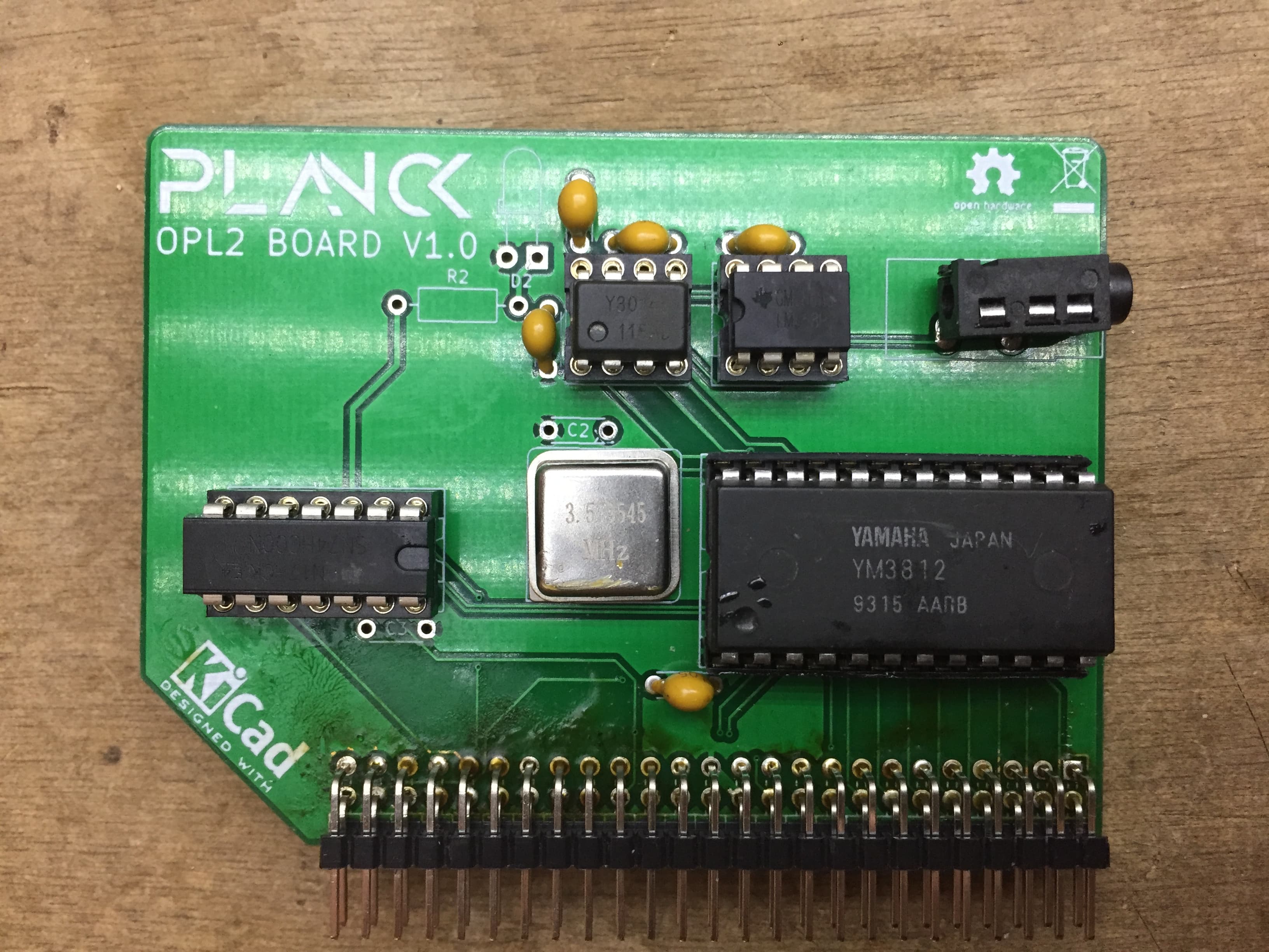
Planck board is an open-source printed circuit board by douggilliland, from the douggilliland/Retro-Computers repository on GitHub. It is a 2-layer board of 80.8 × 60.1 mm with 540 parts on 48 nets, routed with 2 tracks and 0 vias.
It belongs with the retro computing and games boards of this library.
This is a sound card based on the YM3892 OPL2 sound chip.

This documentation is licensed under a Creative Commons Attribution-ShareAlike 4.0 International License.
| Qty | Value | Footprint | References |
|---|---|---|---|
| 1 | Conn_01x40 | Connector_PinHeader_2.54mm:PinHeader_2x25_P2.54mm_Horizontal | J1 |
The 1 most common of 540 parts.

douggilliland/Retro-Computers
Retro-Computer Designs (Z80, 65C816, etc)


SolderedElectronics/Soldered-Inkplate-6-COLOR-hardware-design
Hardware design, BOM, gerbers and 3D files for Soldered-Inkplate-6-COLOR designed by Soldered Electronics.


ADFTech/xtec-uc-ip-main-pcb
KiCad hardware repo for the UC-IP main PCB (currently: IOB board family). This README documents the review-and-release process used to get a schematic/PCB change from an engineer's desk to fabrication.


ulikoehler/OpenPowerDistributor
Open-hardware PCB to distribute DC 12V power to 12V / 5V / 9V & 24V consumers
It measures 80.8 × 60.1 mm and has 2 copper layers, 1.6 mm thick.
540 parts. The full list of its parts is on this page, with links to each part's symbol and footprint where PCBKit's library has them.
From the douggilliland/Retro-Computers repository on GitHub, at the commit this page was made from: the board is 6502/planck-6502/Hardware/proto_board/planck_board.kicad_pcb. PCBKit opens the board in the browser, with nothing to install.
Its repository states no licence, so its author keeps all rights: ask douggilliland before reusing the design.