2 layers85.6 × 54 mm
 dossalab/random-pcbs
Random PCBs I have at my disposal
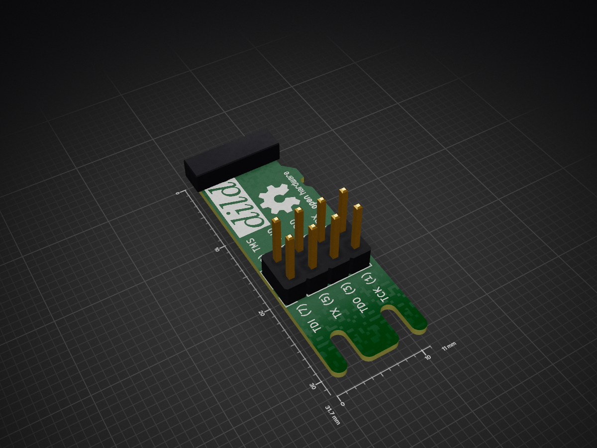
Sd card debug is an open-source printed circuit board by dossalab, from the dossalab/random-pcbs repository on GitHub. It is a 2-layer board of 11 × 31.7 mm with 3 parts on 8 nets, routed with 27 tracks and 0 vias.
These things are too minor to create separate repositories for them.
| Name | Description | Notes |
|---|---|---|
| ips-display-breakout | Breakout for ST7789-based 240x240 IPS display from Aliexpress | |
| library | Directory containing common footprints & libraries | |
| nrf-card | Development board in a size of a credit card containing NRF52832, SD card breakout, ST7789-based display and more | This was done before I discovered that NRF52 consumes 32 uA of current, so it has external RTC and unnecessary powerup logic. |
| sd-card-debug | SD/MMC card breakout board intended for JTAG debugging on Rockchip / Alwinner boards | Codename "dildo" - never ordered |
| Qty | Value | Footprint | References |
|---|---|---|---|
| 1 | Conn_02x04_Odd_Even | Connector_PinHeader_2.54mm:PinHeader_2x04_P2.54mm_Vertical | J3 |
| 1 | Micro_SD_Card | sd-card:microsd | J1 |
The 2 most common of 3 parts.
It measures 11 × 31.7 mm and has 2 copper layers, 0.8 mm thick.
3 parts. The full list of its parts is on this page, with links to each part's symbol and footprint where PCBKit's library has them.
From the dossalab/random-pcbs repository on GitHub, at the commit this page was made from: the board is sd-card-debug/sd-card-debug.kicad_pcb and its schematic ips-display-breakout/display-breakout.kicad_sch. PCBKit opens the board in the browser, with nothing to install.
Its repository states no licence, so its author keeps all rights: ask dossalab before reusing the design.


hzeller/rpi-rgb-led-matrix
Controlling up to three chains of 64x64, 32x32, 16x32 or similar RGB LED displays using Raspberry Pi GPIO


atopile/atopile
Design circuit boards with code! ✨ Get software-like design reuse 🚀, validation, version control and collaboration in hardware; starting with electronics ⚡️


hackclub/sprig
🍃 Learn to code by making games in a JavaScript web-based game editor.