Skip to the content
2 layers76.2 × 40.6 mmEspressifESP32toExpressAdaptor, the printed circuit board in 3D

EspressifESP32toExpressAdaptor

dnhutchins/ETC_Express_Reverse_Eng5

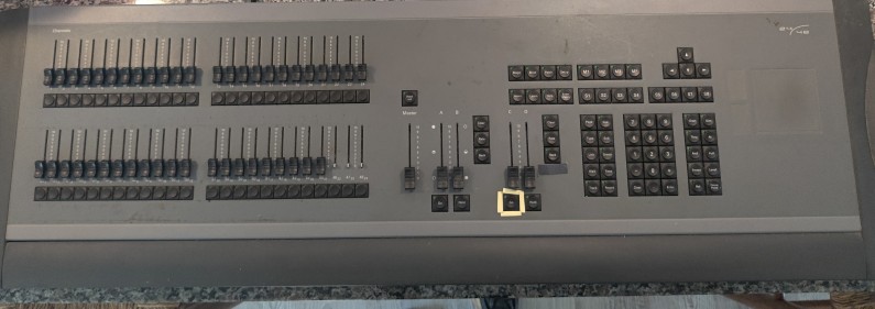
The ultimate goal of this work is to develop an interface to use the control surface from a legacy ETC Express 24/48 lighting controller as a modern EOSNomad compatible programming and fader wing.

Size
76.2 × 40.6 mm
Copper layers
2
Thickness
1.6 mm
Parts
3
Nets
44
Pads
80
Tracks, vias
169, 20
Pours
2
Routed
Yes
KiCad
KiCad 8.0 (file 20240108)
Created
11 Jan 2025
Updated
19 Feb 2025

Overview

EspressifESP32toExpressAdaptor is an open-source printed circuit board by dnhutchins, from the dnhutchins/ETC_Express_Reverse_Eng repository on GitHub. It is a 2-layer board of 76.2 × 40.6 mm with 3 parts on 44 nets, routed with 169 tracks and 20 vias.

It is built around the ESP32-S3-DEVKITC-1-N8 and 2PIN. Its parts include 2 connectors and 1 IC. It belongs with the lEDs and displays and interfaces and adapters boards and the ESP32 boards of this library.

Main components

2

README

Readme.md

ETC Express Control Surface Reverse Engineering

ETC Express Control Surface

Introduction

The ultimate goal of this work is to develop an interface to use the control surface from a legacy ETC Express 24/48 lighting controller as a modern EOSNomad compatible programming and fader wing. The CPU platform for the this board is not likely to be re-used for this project. This platform was developed in the late 1900s during the height of the Intel RISC based i960's popularity. This platform has been long abandoned, and although some tool-chains do exist, none seem to have been maintained beyond the early 2000s. As well no modern platform emulators seem to exist for the i960 architecture. Due to these challenges I decided to approach reverse engineering the interface port between the control surface and the CPU module, to hopefully implement either an OCS or HID based interface to a PC running EOS.

Teardown & Analysis

Internal Layout

Internal images are in the folder internal-photos

General System Layout

Overall, the console is comprised of two main components, the CPU/IO module, and the control surface. The two are connected by means of a 34 pin (2x17) connector.

Control Surface

In the case of the 24/48 model I have access to, the surface consists of two main sections. These two sections are internally separate circuits, with each communicating with the CPU board independently.

Fader & Bump Keys

On the left is the 48 fader & bump key module, consisting of 48 carbon film slide potentiometers as well as 48 momentary normally open "bump key" switches. Various multiplexers/decoders are used in conjunction with a PIC module to create a 2-wire communications link that is passed through directly to the CPU module (where it terminates at an Altera Flex FPGA) for decoding. With the bottom row of bump keys, there are 24 in-key LEDs, these are managed using an ICM7218BIPI LED control IC.

Design & Control keys, Master, and Cross faders

On the right is the initial focus of this project. The primary control interface consisting of 70 N/O momentary key switches, 35 in-key LEDs, 5 carbon film slide potentiometers, and a touch-pad. These interface with the CPU module using 8 pins forming an 8 bit data bus, 7 pins as inputs to the 3 primary multiplexers/decoders, and 2 pins for control signals to the MAX150BCPP ADC. The ADC samples the state of the 5 fader potentiometers through a CD74HC4051-EP Analog Multiplexer and Demultiplexer.

CPU Module

This is the "brains" of the lighting console. This is an old embedded Intel design, employing fairly common chipsets for SuperIO, Floppy, Parallel, Ethernet, and VGA. Alongside the more common stuff, is an Altera Flex FPGA that likely handles the more specific stuff like DMX, ETCNet, MIDI, etc.

Original firmware

This project aims to interface with the control surface, and discard the original CPU/IO module, so this is just listed as a reference in-case someone reads this and want's to port Doom to the express series console's CPU module or something.
The last version of the firmware released: Firmware

Circuit Operation (control surface)

Since the two sections of the surface communicate to the CPU independently the will be treated as separate entities here.

Control Section

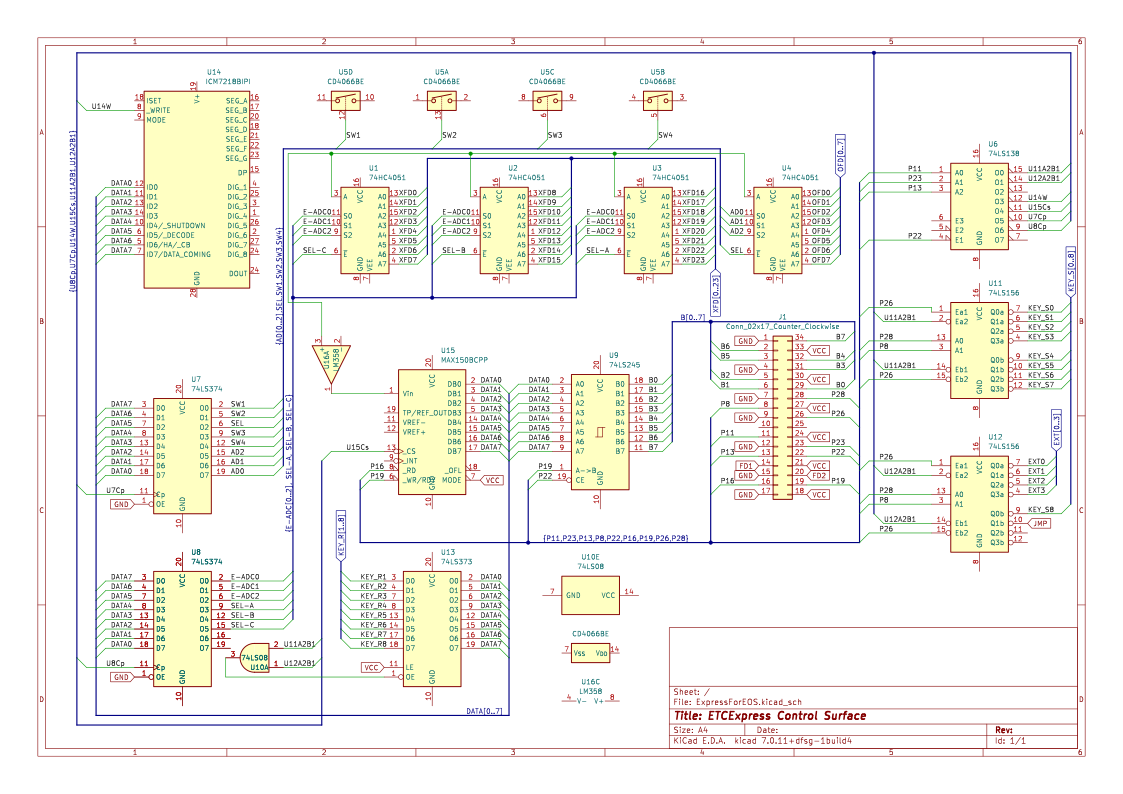
NOTE: This schematic is the product of tracing connections on this circuit, it is only meant to serve as a reference for signaling, it does not include descrete components such as bypass caps, pull up/down resistors, etc.

Schematic There is no external or internal clock signal in this section, states are read/written real-time, and individual ICs are clocked independently using (mostly) seperate signals.

Integrated Circuits
  1. U1-U4 = 74HC4051 (Analog Multiplexer and Demultiplexers) datasheet
  2. U5 = CD4066 (Quad Bilateral Switch) datasheet
  3. U6 = 74LS138 (3-LINE TO 8-LINE DECODERS/DEMULTIPLEXER) datasheet
  4. U7-U8 = 74LS374 (OCTAL EDGE-TRIGGERED FLIP-FLOP) datasheet
  5. U9 = 74LS245 (Octal Bus Transceiver With 3-State Outputs) datasheet
  6. U10 = 74LS08 (Quad 2-Input AND Gate) datasheet
  7. U11-U12 = 74LS156 (DUAL 2-LINE TO 4-LINE DECODERS/DEMULTIPLEXER) datasheet
  8. U13 = 74LS373 (OCTAL D-TYPE TRANSPARENT LATCH) datasheet
  9. U14 = ICM7218 (8 Digit LED Display Driver) datasheet
  10. U15 = MAX150 (CMOS High Speed 8 Bit A/D Converter with Reference and Track/Hold) datasheet
  11. U16 = LM358 (Dual Operational Amplifier) datasheet
8-bit Bus
  1. Connection to the CPU module is buffered via U9.
  2. Pin 19 from the interface connector selects the direction of U9 as well as RD/WR on U15
  3. The bus sets U7 and U8, SN74LS374, to select which CD74HC4051-EP analog multiplexer/demultiplexer is enabled
    • (One mux/demux is used to decode the analog faders, as well as additional mux/demuxes for additional faders not installed in the 24/48 I have access to)
  4. U13 sets the bus, this appears to be used to decode key presses
  5. The bus sets U14 used to drive the in-key leds
  6. U15 sets the bus with value of the fader being routed via the analog mux/demux
Digital Muxes (Addressing and Keyboard scanning)
  1. U6 - SN74LS138 (3-LINE TO 8-LINE DECODERS/DEMULTIPLEXER)
    • This demux is used to signal Write on U14, Cp on U7 and U8, CS on U15, and A2,B1 on either U11 or U12
    • Pins 11, 23, and 13 from the interface connector control the 3 address inputs
    • Pin 22 from the interface connector controls enable for U6 as well as U9
    • When either U11 or U12 is selected, U13 is activated via one of U10s AND gates, to latch key presses to the bus.
  2. U11 - SN74LS156 (DUAL 2-LINE TO 4-LINE DECODERS/DEMULTIPLEXER)
    • Selects one of 8 keyboard "rows"
    • Pins 8, 26, and 28 from the interface connector control the 3 address inputs
    • Chip enable is from U6/0
  3. U12 - SN74LS156 (DUAL 2-LINE TO 4-LINE DECODERS/DEMULTIPLEXER)
    • Selects one of 8 keyboard "rows" (4 of which route to the extrenal connector for a larger board configuration)
    • Pins 8, 26, and 28 from the interface connector control the 3 address inputs
    • Chip enable is from U6/1
Control Latches (Analog mux selection, addressing, and TP switching)
  1. U7 - 74LS374 (OCTAL EDGE-TRIGGERED FLIP-FLOP) Control register
    • Operates SW1-4 of U5 CD4066 Quad Bilateral Switch
    • Address and selection signals to U4 Analog Multiplexer (Responsible for on-board faders and touch pad)
  2. U8 - 74LS374 (OCTAL EDGE-TRIGGERED FLIP-FLOP) Control register
    • Address and selection signals to U4 Analog Multiplexer (Responsible for off-board faders, unused "external" connector
Keyboard "Column" Latches
  1. U13 - 74LS373 (OCTAL D-TYPE TRANSPARENT LATCH)
    • U13 enables output to the bus, of the 8 columns for the row selected by U11/U12
    • This is enabled in the unlatched "following" state whenever either U11/U12 is selected by U6
    • LE is tied to VCC, so there is no actual latching, just switching the keyboard columns onto the bus.
Analog Muxes (Fader Section)
  1. U1-U4 - 74HC4051 (Analog Multiplexer and Demultiplexers)
    • Faders are sampled using a single ADC, the analog muxes U1, U2, U3 and U4 are used to route one of up to 32 faders to the ADC.
    • U1, U2, and U3 all route to the external (unused on my board) connector.
    • U4 is connected to the Master, A, B, C, and D faders, as well as the touchpad.
    • U5 (quad analog switch) plays a role in routing the touch pad, where 2 of the switches short short the signal sides, including either pin 2 or 4 of U4 to ground, while the other switch on/off VCC (through a pull up resistor) to the other sides of the touch pad.
    • The output of the mux is connected to U15 through U16, to be sampled.
ADC
  1. U15 - MAX150
    • Pin 16 from the interface connector controls the RD signal to the ADC
    • CS is driven from U6
    • Data is put directly on the bus
    • WR/WR follows the control from P19 along with the the buffer U9
LED Driver
  1. U14 - ICM7218 (8 Digit LED Display Driver)
    • Pin 28 from the interface connector controls the MODE signal
    • U6/3 controls the WRITE signal
    • Mode is raised to send control word, then lowered to pulse in each of the 8 banks of 8 leds

34-pin "Face Panel Bus" Connector

This is the interface between the control surface and the CPU. The pins of this connector are connected internally as follows:

Pinout

  1. GND
  2. U9 Pin-12 (B7)
  3. U9 Pin-13 (B6)
  4. GND
  5. U9 Pin-16 (B3)
  6. U9 Pin-17 (B2)
  7. GND
  8. U11 & U12 Pin-3 (B)
  9. GND
  10. N/C
  11. U6 Pin-1 (A)
  12. GND
  13. U6 Pin-3 (C)
  14. FADER-SUB-BOARD Data (PIC micro on fader board)
  15. GND
  16. U15 Pin-8 (_RD)
  17. GND
  18. VCC
  19. U15 Pin-6 (_WR/RDY)
  20. FADER-SUB-BOARD Data (PIC micro on fader board)
  21. VCC
  22. U6 Pin-4 (G1)
  23. U6 Pin-2 (B)
  24. VCC
  25. N/C
  26. U11 & U12 Pins-1,15 (1C,2C)
  27. VCC
  28. U11 & U12 Pin-13 (A)
  29. U9 Pin-18 (B1)
  30. VCC
  31. U9 Pin-15 (B4)
  32. U9 Pin-14 (B5)
  33. VCC
  34. U9 Pin-11 (B8)

Misc. Links

https://github.com/ETCLabs/lighthack/?tab=readme-ov-file

Parts

3
QtyValueFootprintReferences
12pinConnector_PinHeader_2.54mm:PinHeader_1x02_P2.54mm_VerticalJ1
1Conn_02x17_Odd_EvenConnector_IDC:IDC-Header_2x17_P2.54mm_VerticalJ3
1ESP32-S3-DevKitCPCM_Espressif:ESP32-S3-DevKitCU2

Similar boards

  • 2 layers39.5 × 64.7 mmTesty, the printed circuit board in 3D

    Testy

    mmalex/wookash_thing

    a small rp2040 based thing for a livestream with wookash

    65 parts10MIT
  • 4 layers44.9 × 47.2 mmThermalCam, the printed circuit board in 3D

    ThermalCam

    randomplum/autoliv_nv3_uvc

    Adapter for the Autoliv NV3 sensor providing USB video device class output

    131 parts9
  • 2 layers45 × 100 mmGaggiaBoard V3, the printed circuit board in 3D

    GaggiaBoard V3

    SomeLucky1/CoffeeHat

    Basic espresso machine controls based on Arduino Nano extension board.

    80 parts2CC0-1.0
  • 2 layers98 × 98 mmMaglock, the printed circuit board in 3D

    Maglock

    makerspacelt/maglock-hw

    MagLock is the entrance controller hardware. It features:

    221 parts
  • 2 layers70 × 57.5 mmG474-CAN universal, the printed circuit board in 3D

    G474-CAN universal

    rkhk-gears/pcbs

    These designs are provided as-is and may be subject to changes.

    223 parts
  • 2 layers40.5 × 55.4 mmRP AMC3302 Zu, the printed circuit board in 3D

    RP AMC3302 Zu

    ZivojinV/AMC3302

    Custom AMC3302-based Precision Full-Wave Rectifier Analog PCB

    62 parts
  • 2 layers109 × 99 mmUrx, the printed circuit board in 3D

    Urx

    HolTyc/Urx_documentation

    Ultimate retro box - arduino 3D printed 16x16 red dot game console

    11 parts2

Questions

How big is the EspressifESP32toExpressAdaptor PCB?

It measures 76.2 × 40.6 mm and has 2 copper layers, 1.6 mm thick.

What parts does the EspressifESP32toExpressAdaptor use?

3 parts, built around the ESP32-S3-DEVKITC-1-N8 and 2PIN. The full list of its parts is on this page, with links to each part's symbol and footprint where PCBKit's library has them.

Where can I download the EspressifESP32toExpressAdaptor KiCad files?

From the dnhutchins/ETC_Express_Reverse_Eng repository on GitHub, at the commit this page was made from: the board is kicad/EspressifESP32toExpressAdaptor/E/E.kicad_pcb and its schematic kicad/EspressifESP32toExpressAdaptor/E/E.kicad_sch. PCBKit opens the board in the browser, with nothing to install.

Can I use the EspressifESP32toExpressAdaptor design in my own project?

Its repository states no licence, so its author keeps all rights: ask dnhutchins before reusing the design.