2 layers39.9 × 46.4 mm
CrealityDryerV1
Ermakov/CrealitySpacePiAutomation
Creality Space Pi Plus CFS mod automation (PCB and sketch for Arduino IDE)
20 parts33
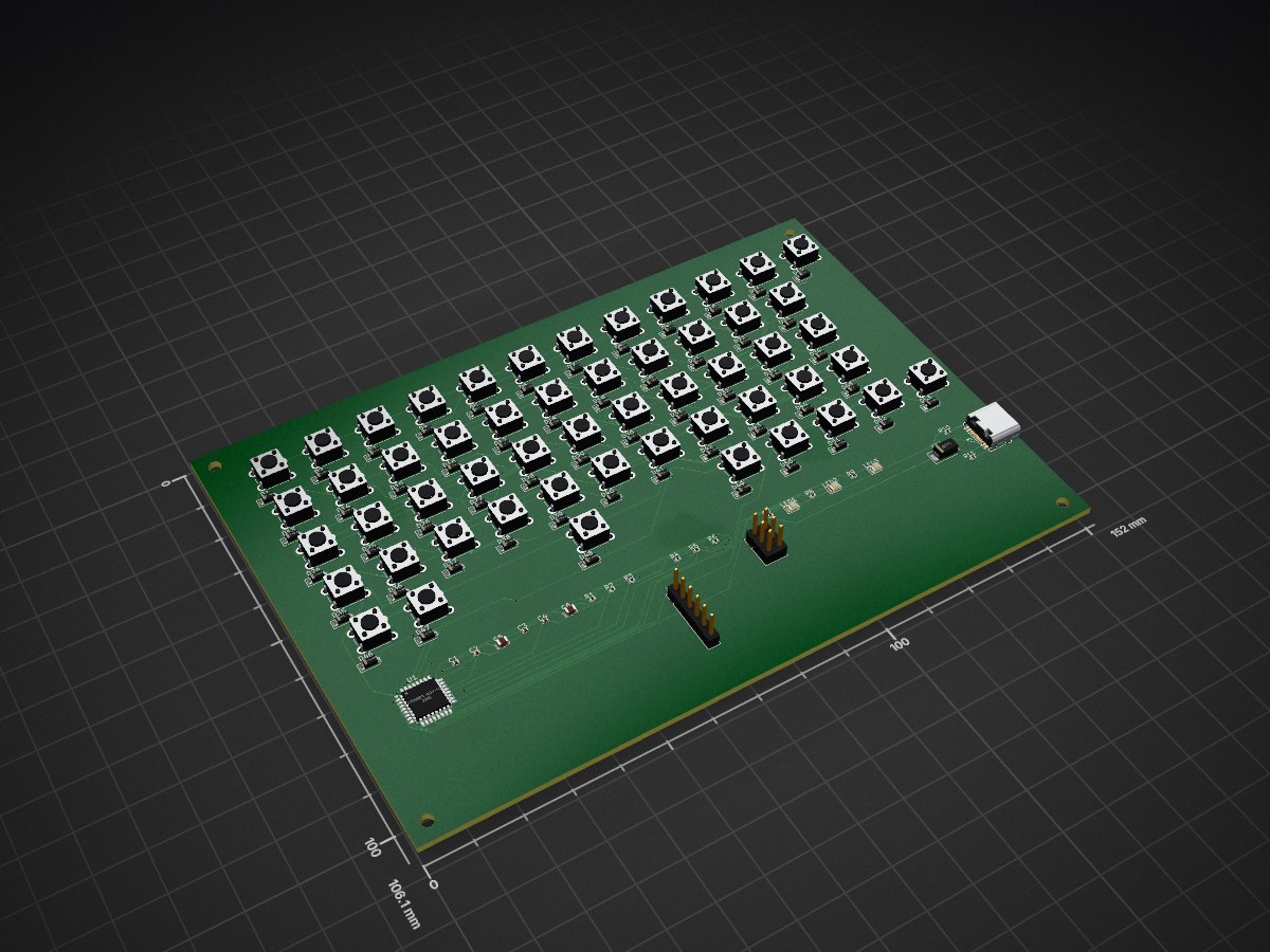
 dmang-dev/workboy
Open, buildable recreation of Nintendo's unreleased Game Boy WorkBoy keyboard: firmware, clean-room ROM, DRC-clean PCB, 3D case, CI
Workboy is an open-source printed circuit board by dmang-dev, from the dmang-dev/workboy repository on GitHub, published under the MIT licence. It is a 2-layer board of 152 × 106.1 mm with 135 parts on 89 nets, routed with 951 tracks and 60 vias.
It is built around the ATMEGA328P-AU, 1N4148W and SS14. Its parts include 57 diodes, 53 switches, 11 resistors, 6 capacitors and 3 connectors. It belongs with the retro computing and games and keyboards and input boards and the AVR (ATmega, ATtiny) boards of this library.


An open recreation of Nintendo's unreleased Game Boy WorkBoy keyboard accessory (Source R&D / Fabtek / Montague‑Weston, 1992): a QWERTY keyboard that plugs into the Game Boy Link Port and turns the console into a PDA, plus a software cartridge.
This repo contains a complete, buildable and CI‑verified design — firmware, a clean‑room ROM, a DRC‑clean PCB, a 3D‑printed case, and an assembly‑ready BOM.
Status:
python tests/run_ci.pyis green — 16 protocol checks + ROM, firmware, and case builds. The PCB autoroutes to 0 DRC violations.
| Path | What |
|---|---|
BUILD_PLAN.md | the full engineering plan (start here) |
WORKBOY_PROTOCOL.md | the link‑port byte protocol + scan‑code table |
layout/ | single source of truth for the 53‑key layout (keymap.py) |
firmware/ | ATmega328P keyboard firmware (PlatformIO / avr‑gcc) |
rom/ | clean‑room GBDK cartridge: notepad, clock, calculator, phone book |
kicad/ | netlist, placed+routed board, Gerbers, CPL — see PCB_README.md |
case/ | parametric enclosure (OpenSCAD + build123d) |
tests/ | protocol_sim.py + run_ci.py; CI in .github/workflows/ |
python tests/run_ci.py # runs every check whose toolchain is installedToolchains: GBDK‑2020 (ROM), PlatformIO + avr‑gcc (firmware), build123d (case),
KiCad 10 + Freerouting (PCB). See BUILD_PLAN.md and
kicad/PCB_README.md for the full pipelines.
The Game Boy is the serial master on the link port; the WorkBoy keyboard is a passive slave that returns one scan‑code byte per poll. So the "custom PCB" is a small 5 V ATmega328P keyboard‑matrix controller that speaks the documented WorkBoy serial protocol — no level shifter needed. The protocol/scan‑codes were reverse‑engineered by shonumi (GBE+) and re‑verified here against the real ROM.
One 5 V design covers every console that can run a Game Boy / Game Boy Color cartridge — including the GBA and GBA SP, whose link port switches to 5 V when an 8‑bit cartridge is inserted. Only the cable plug varies.
| Works | Doesn't |
|---|---|
| DMG‑01, Pocket, Light, Color, GBA, GBA SP | Game Boy Micro (GBA‑only, can't run GB/GBC carts) · Super Game Boy (no link port) |
Full table, cable choices, and why this is not split into per‑console repos:
COMPATIBILITY.md.
⚠️ GBA/SP support is documented behaviour that this project has not yet verified on a bench. Measure before trusting it.
Nothing here is exotic. Rough 2026 USD; the board is most of the cost.
Console side
| Item | Why | ~$ |
|---|---|---|
| A Game Boy that runs GB/GBC carts | the target console — see the compatibility table above | — |
| Flash cart + microSD (EZ-Flash Junior, EverDrive GB, …) | runs rom/workboy_homebrew.gb. SD-backed saves mean the phone book persists with no cart battery | 25–70 |
| A cheap DMG/GBC link cable to cut | the plug end is the connector — see below | 5–8 |
The keyboard board
| Item | Why | ~$ |
|---|---|---|
| Bare PCB from JLCPCB, qty 10 | zip up kicad/gerber/ and upload it. ~$19.60 + shipping | 48 |
Components per workboy_jlcpcb_bom.csv | one 100-pc lot of each resistor value covers the run. The ATmega is 55 % of it | 39 |
| ~60× 6×6 mm THT tact switches (LCSC C42416249) | the 53 keys + spares. ⚠️ Not C720477 — that is an SMD 4×3 mm part and will not fit | 2 |
| 2×3 2.54 mm pin header | the ISP header (J2), for flashing | 1 |
| M2.5 brass heat-set inserts + screws | fasten the printed clamshell | 10 |
| (optional) blank tactile keycaps | nicer than printed; legends are non-standard anyway | 6 |
Ordering 10 boards costs $86.50 all-in ($8.65/board) versus $59.75 for 5 — 28 % cheaper per board, because the engineering fee and shipping don't scale.
Tools
firmware/platformio.ini already ships a commented stk500v1 block for
the Arduino-as-ISP path.The link connector — the one part with no catalog option There is no reliably-purchasable bare DMG link plug. Either cut a third-party link cable (most reliable — keep the 4 used wires SO/SI/SC/GND, and meter them before soldering: the two ends are deliberately cross-wired, so one end's SO is the other's SI), or 3D-print the plug — e.g. svender's DMG link cable plug, which uses 6 pins harvested from female USB sockets. Breakout PCBs exist but still need a cable.
Suggested order of purchase. Buy the logic analyzer and a link cable first and run the P0/P1 protocol test on a breadboard — prove the handshake before spending on the PCB. Order boards, switches and inserts only once that works.
MIT — see LICENSE. Attribution, scope, and what is deliberately
not in this repo are recorded in NOTICE.
This is an independent, unofficial recreation. It is not affiliated with, endorsed by, or connected to Nintendo, Source R&D, Fabtek, or Montague‑Weston. "WorkBoy" and "Game Boy" are used descriptively to identify the device being recreated and the consoles it attaches to.
The original WorkBoy ROM is leaked, copyrighted Nintendo‑licensed code — it is
not included here and must not be committed or distributed. The cartridge
software in rom/ is clean‑room, written from the documented wire protocol.
Use the leaked ROM only for private bench reference.
The WorkBoy trademark (USPTO 74239332, filed 1992) was abandoned in 1994
without ever registering, and both original companies are defunct — see
NOTICE.
| Qty | Value | Footprint | References |
|---|---|---|---|
| 53 | 1N4148W | D_SOD-123 | D1, D2, D10, D11, D12, D13, D14, D15, D16, D17, D18, D19, D20, D21, D22, D23 +37 |
| 53 | TACT_6mm | SW_PUSH_6mm | SW1, SW2, SW10, SW11, SW12, SW13, SW14, SW15, SW16, SW17, SW18, SW19, SW20, SW21, SW22, SW23 +37 |
| 4 | 100nF | C_0402_1005Metric | C1, C2, C3, C4 |
| 4 | MountingHole_M2.5 | MountingHole_2.7mm_M2.5 | H1, H2, H3, H4 |
| 3 | 10k | R_0402_1005Metric | R1, R2, R3 |
| 3 | 1k | R_0402_1005Metric | R7, R8, R9 |
| 3 | 220 | R_0402_1005Metric | R4, R5, R6 |
| 2 | 10uF | C_0805_2012Metric | C5, C6 |
| 2 | 5.1k | R_0402_1005Metric | R10, R11 |
| 2 | GREEN | LED_0805_2012Metric | LED2, LED3 |
| 1 | ATmega328P-AU | TQFP-32_7x7mm_P0.8mm | U1 |
| 1 | GB-LINK | PinHeader_1x06_P2.54mm_Vertical | J1 |
| 1 | ISP-2x3 | PinHeader_2x03_P2.54mm_Vertical | J2 |
| 1 | RED | LED_0805_2012Metric | LED1 |
| 1 | SS14 | D_SMA | D54 |
| 1 | USB-C-16P | USB_C_Receptacle_HRO_TYPE-C-31-M-12 | J3 |
It measures 152 × 106.1 mm and has 2 copper layers, 1.6 mm thick.
135 parts, built around the ATMEGA328P-AU, 1N4148W and SS14. The full list of its parts is on this page, with links to each part's symbol and footprint where PCBKit's library has them.
From the dmang-dev/workboy repository on GitHub, at the commit this page was made from: the board is kicad/workboy.kicad_pcb. PCBKit opens the board in the browser, with nothing to install.
Its repository publishes it under the MIT licence: you may reuse it on that licence's terms (keep the author's notice, and for a copyleft licence share your changes alike).
Ermakov/CrealitySpacePiAutomation
Creality Space Pi Plus CFS mod automation (PCB and sketch for Arduino IDE)


jayanta525/dual-h-bridge
Dual H-Bridge Controller with IRF3205 and IR2104 MOSFET Driver, and with ATMega328P-AU PWM Controller

d-diot/Mini-BT-Pcb-328P
MySensors ATMega328P + RFM69 and NRF24 battery (AAA and CR2032) powered pcb

Alihk93/B-W_Master_Slave_RF
Design, validate, and release two manufacturable PCBs that together form a one-way wireless link: a solar-powered remote node (**R_Slave**) transmits a 433.92 MHz ASK/OOK signal to a mains-powered base unit…

lizard-electronics/Soldering_Fume_Extractor
Portable soldering fume extractor based on an ATmega328P MCU.

