
2 layers327.9 × 139 mm
Coco2
baldengineer/bit-preserve
Project for capturing vintage, classic, aka old computer schematics in KiCad.
147 parts446

 djarty24/miffy-blinky
My first PCB project! I made this following Hack Club's Stasis starter project guide on making a blinky.
Miffy blinky is an open-source printed circuit board by djarty24, from the djarty24/miffy-blinky repository on GitHub. It is a 2-layer board of 65.3 × 91.9 mm with 18 parts on 18 nets, routed with 208 tracks and 0 vias.
It is built around the NE555P. Its parts include 10 diodes, 2 capacitors, 2 resistors, 2 ICs and 1 connector.
This is my first PCB project. I made a custom Miffy-shaped blinky keychain following Hack Club's Stasis project started guide!
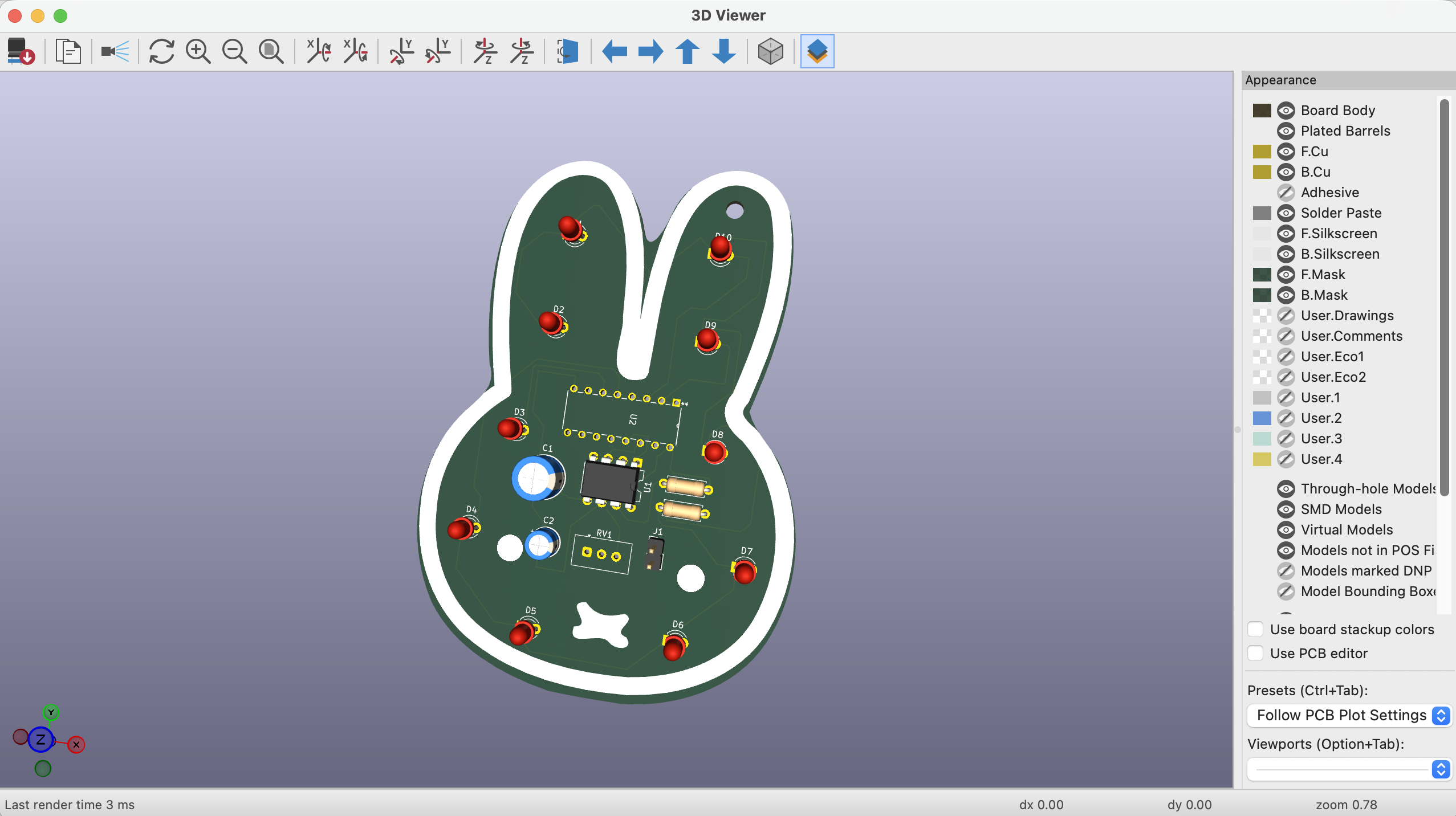
Coming from mostly web dev and frontend stuff, jumping into KiCad was definitely an experience. It turns out making a PCB is basically like doing UI design, except the components actually take up physical space and you can't just z index them away lol.
Super proud of how this turned out!
I finally finished my first ever custom hardware project! I made a PCB shaped like Miffy, one of my favorite characters, that also doubles as a keychain.
The first step is in the schematic editor of KiCad to design the circuit. Here, I placed symbols for the 555 timer, a 4017 counter, a power bank, two capacitors, two resistors, and 10 LEDs.
In my Principles of Engineering class in school, we briefly covered circuitry, but I was under the assumption that everything needs to be connected. However, something cool I learned was using labels. This kept my schematic design cleaner and more readable.
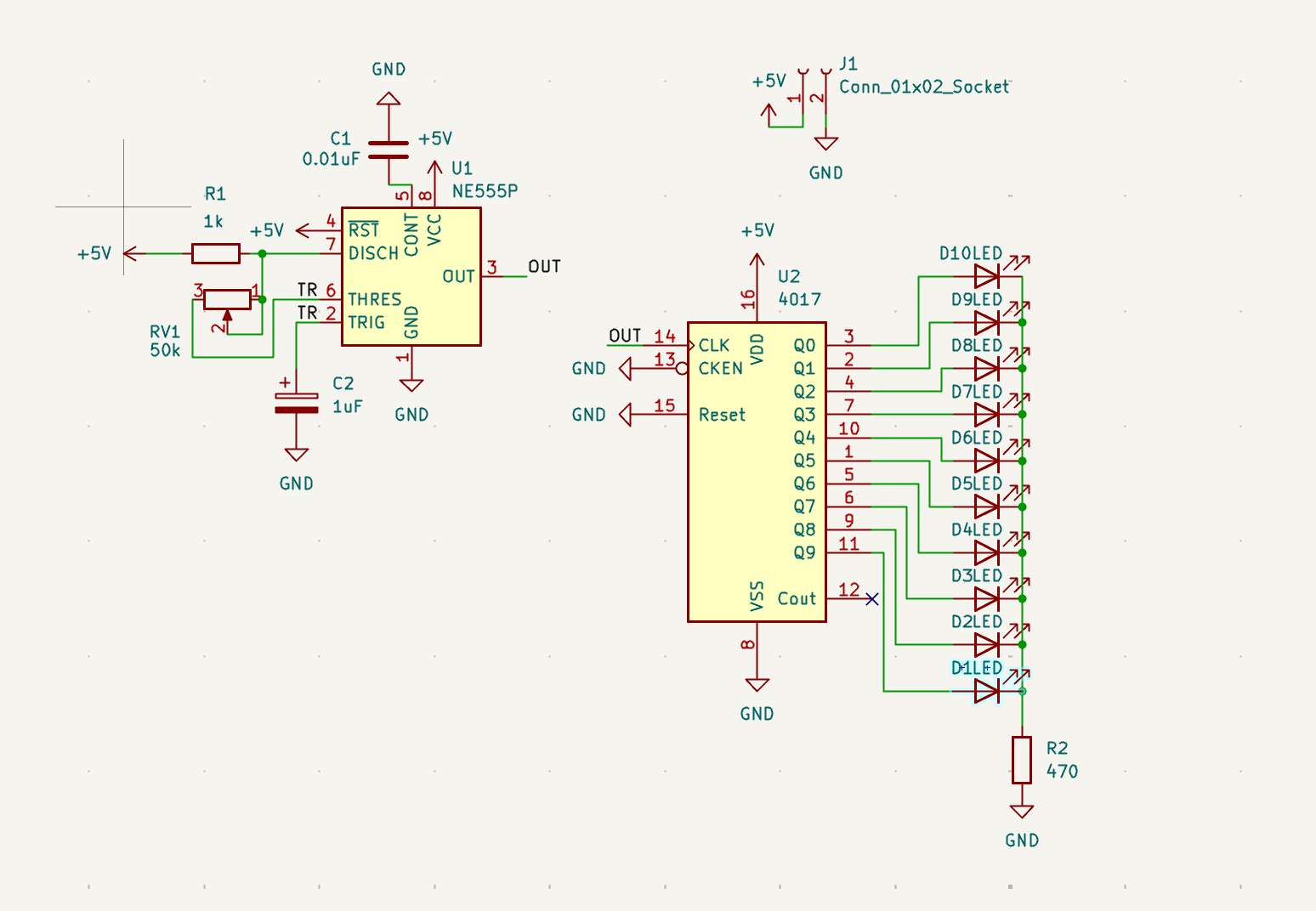
I followed the guide to add the custom 4017 counter footprint to my project. Then, I switched to the PCB view, only to find that I couldn't actually move the LEDs. After a lot of troubleshooting, I realized that I hadn't added any footprints for the rest of my components like the actual LEDs.
This was the most fun part!
Now that the footprints were installed, I uploaded a DXF file of Miffy. I learned about grouping and ungrouping and how to set each part of her face on the correct layer. I changed the border to be an Edge Cut for the outline of the PCB. Then, I placed the components and LEDs where I wanted on the board.
Now that everything was positioned where I wanted it to be, I had to replace the ratsnets with copper tracks. This was both therapeutic and frustrating at times because you can't have two lines of the same color cross. When a red track blocked my path, I switched to the blue layer and vice versa.
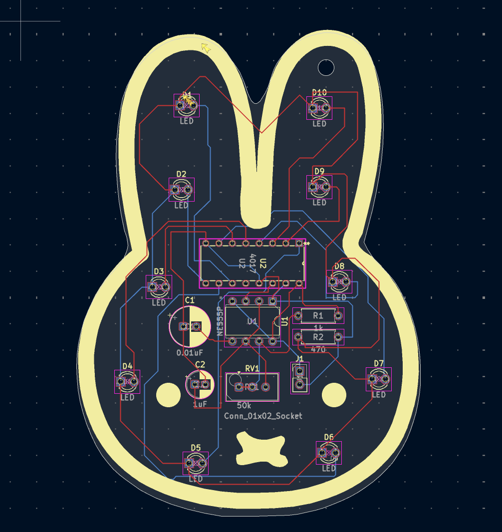
The Design Rules Checker tool was extremely helpful because it helped me catch mistakes I made.
Finally, I added another hole from the Edge Cuts layer with a diameter of 1.5 mm to serve as the hole where I can insert my keychain later. I also converted Miffy's eyes and mouth into Polygons (this took a lot longer than expected) and filled them in.
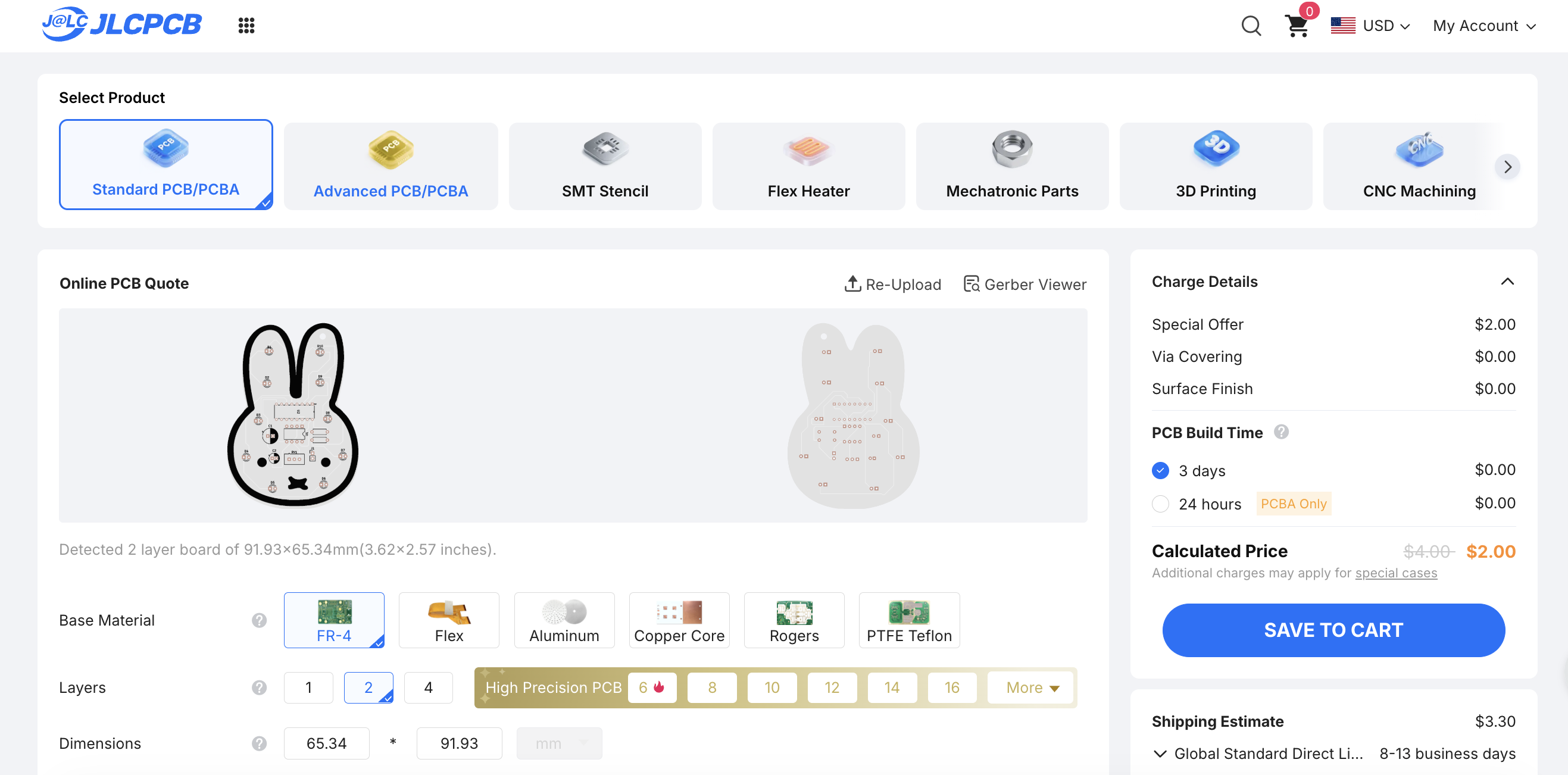
This was the last step, I just generated the gerber and drill files and saved them into a zip. Then, I went to JLCPCB to get a price estimate. I changed the color of my PCB to white, and so the drawings turned black, so it actually looks pretty similar to the original Miffy character!
I also pushed my files to GitHub and wrote up a quick README for my project.
This was my first time working with PCBs and it was an awesome experience. Designing a physical object that I can hold in my hands is completely different from anything I've done before since I usually just write software. I learned a lot about designing readable schematics and positioning them on the actual PCB.
Even though there was a huge learning curve and a fair share of frustrating moments, I learned a lot and it was really fun!
I had so much fun building this Miffy blinky keychain and I'm definitely going to design more PCBs in the future!
| Qty | Value | Footprint | References |
|---|---|---|---|
| 10 | LED | LED_THT:LED_D3.0mm | D1, D2, D3, D4, D5, D6, D7, D8, D9, D10 |
| 1 | 0.01uF | Capacitor_THT:CP_Radial_D7.5mm_P2.50mm | C1 |
| 1 | 1k | Resistor_THT:R_Axial_DIN0207_L6.3mm_D2.5mm_P7.62mm_Horizontal | R1 |
| 1 | 1uF | Capacitor_THT:CP_Radial_D5.0mm_P2.00mm | C2 |
| 1 | 4017 | Custom_Imports:N16 | U2 |
| 1 | 470 | Resistor_THT:R_Axial_DIN0207_L6.3mm_D2.5mm_P7.62mm_Horizontal | R2 |
| 1 | 50k | Potentiometer_THT:Potentiometer_Vishay_T93YA_Vertical | RV1 |
| 1 | Conn_01x02_Socket | Connector_PinHeader_2.54mm:PinHeader_1x02_P2.54mm_Vertical | J1 |
| 1 | NE555P | Package_DIP:DIP-8_W7.62mm | U1 |
baldengineer/bit-preserve
Project for capturing vintage, classic, aka old computer schematics in KiCad.

The-Invent0r/8-bit-Computer-PCB
These are the KiCAD files for my 8-Bit Computer.

DarcyJProjects/touchtone555
An open-source DIY, NE555-based analogue synthesizer - play notes with a stylus


benjiaomodular/SynthCard
I designed this project with the help of PCBWay. You can get a copy of these cards through the PCBWay Shared Projects page.

fortinsylvain/MyCpu
Home brew CPU Hardware with 1-bit ALU implementation using 74LSxx, a micro-code and assembler coded in C#.

hackup/C128Diag
Replica of the Commodore C128 Diagnostic Test cartridge Assy No. 325093-01.
It measures 65.3 × 91.9 mm and has 2 copper layers, 1.6 mm thick.
18 parts, built around the NE555P. The full list of its parts is on this page, with links to each part's symbol and footprint where PCBKit's library has them.
From the djarty24/miffy-blinky repository on GitHub, at the commit this page was made from: the board is miffy-blinky.kicad_pcb and its schematic miffy-blinky.kicad_sch. PCBKit opens the board in the browser, with nothing to install.
Its repository states no licence, so its author keeps all rights: ask djarty24 before reusing the design.