2 layers99.5 × 83.1 mm

 djarty24/keeb
Hack Club Keeb custom keyboard
Keeb is an open-source printed circuit board by djarty24, from the djarty24/keeb repository on GitHub. It is a 2-layer board of 317.9 × 129.1 mm with 166 parts on 117 nets, routed with 772 tracks and 0 vias.
It belongs with the keyboards and input boards and the RP2040 boards of this library.
Just found out about Hack Club Keeb! I wanted to get started with this challenge.
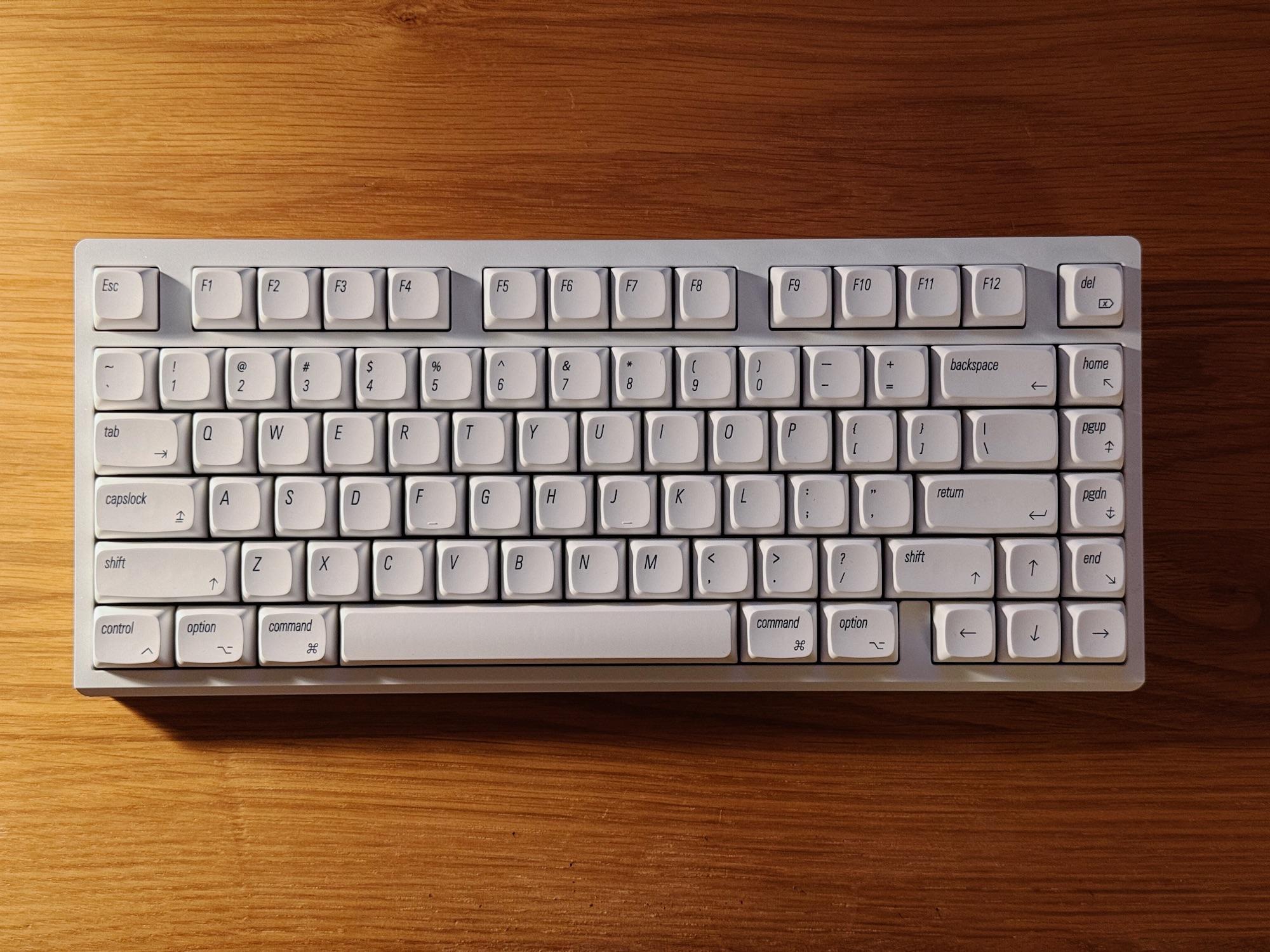
I first read through the Planning Your Keyboard section in the docs and started brainstorming what I wanted my keyboard to look like. After doing some research, I've decided on a 75% layout for my Mac. I want it to look pretty standard, like this image:
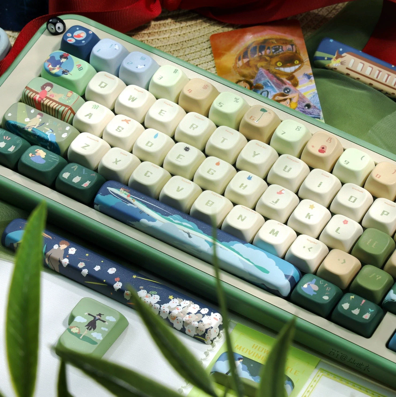
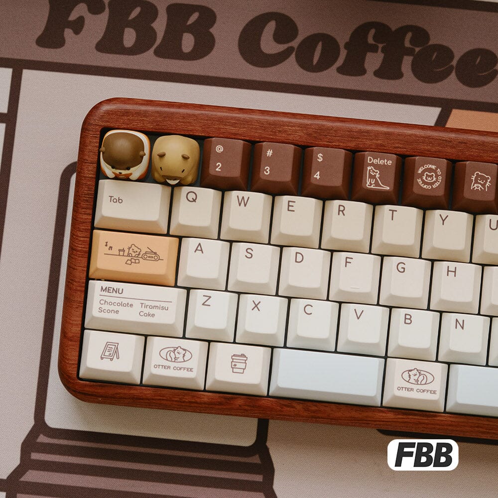
The personalization will be through the keycaps! I'll also add fun illustrations on the PCB silkscreen. I'm thinking of designing my own Monet themed keycaps or purchasing custom ones off of Etsy like the following:
As for the case, I want it to have slight borders around everything and larger borders to separate the arrow keys and function row like the first image displayed.
Esc   F1 F2 F3 F4   F5 F6 F7 F8   F9 F10 F11 F12   Power

`  1  2  3  4  5  6  7  8  9  0  -  =   Backspace     Home
Tab Q  W  E  R  T  Y  U  I  O  P  [  ]   \          PgUp
Caps A  S  D  F  G  H  J  K  L  ;  '   Return       PgDn
Shift Z  X  C  V  B  N  M  ,  .  /   Shift   ↑      End
Ctrl Opt Cmd        Space        Cmd Opt     ← ↓ →
Design Time: ~90 min
Next, I moved on to the Desighing the PCB section in the docs.
I've decided on linear switches since they seem to be the quietest and best for wrist health.
Initially I was pretty confused with how to even get started. So I headed over to YouTube and watched a tutorial by Joe Scotto that explained direct vs. matrix wiring. Looking at my reference image, my keyboard needs 15 columns and 6 rows, which means my microcontroller needs at least 21 pins. This fits perfectly within the Raspberry Pi Pico's 26 GPIO pins!
Now, it was time to open up KiCAD and get started.
In the tutorial, it said I would need stabilizers for keys larger than 2u. So what I did next was identify the size of each key. Most keys were 1u, however some exceptions:
Tab: 1.5u Caps Lock: 1.75u Left Shift: 2.25u Right Shift: 1.75u Backslash: 1.5u Return: 2.25u Backspace: 2u Space: 6.25u Ctrl/Opt/Cmd/Right Cmd/1.25u
My eyes hurt really bad after squinting over the reference image but I believe this is right. So, the only keys that I need stabilizers for are Left Shift, Return, Backspace, and Space.
Then I created one row of keys.
Today, I continued working on the PCB. I finished up adding all of the key-diode units and orienting them to match my physical keyboard inspo. Although it isn't perfectly aligned it should be good enough to move on to the next step. Here's what my matrix looked like:
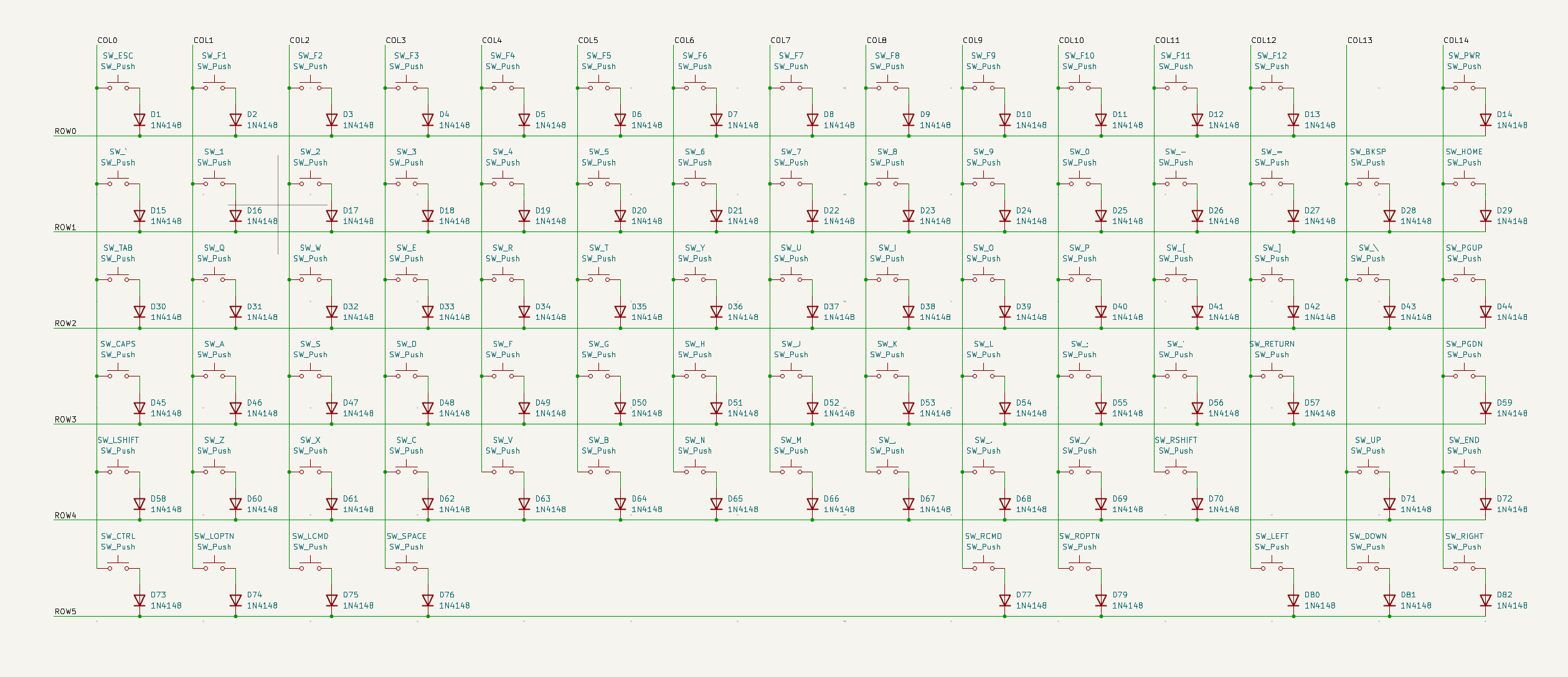
Next, I added in the Pico and added labels to its GPIO pins. I also added the stabilizers and 5 mounting holes as well.
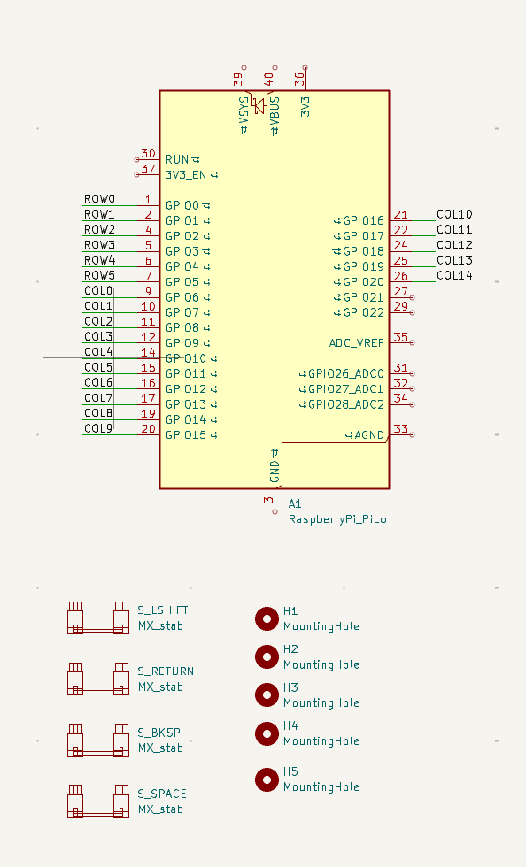
Now, it was time to move on to the next step!
THIS TOOK ME 8 HOURS. I don't have many screenshots since I was pretty locked in but I had to manually orient every single switch-diode unit to match the exact layout I wanted. The grid system in KiCad is pretty bad, so I calculated all of the X-Y coordinates of all 81 keys using a formula I made on Desmos and positioned them accordingly. Then, I placed the diodes and routed all of my traces. This is what it looks like now:
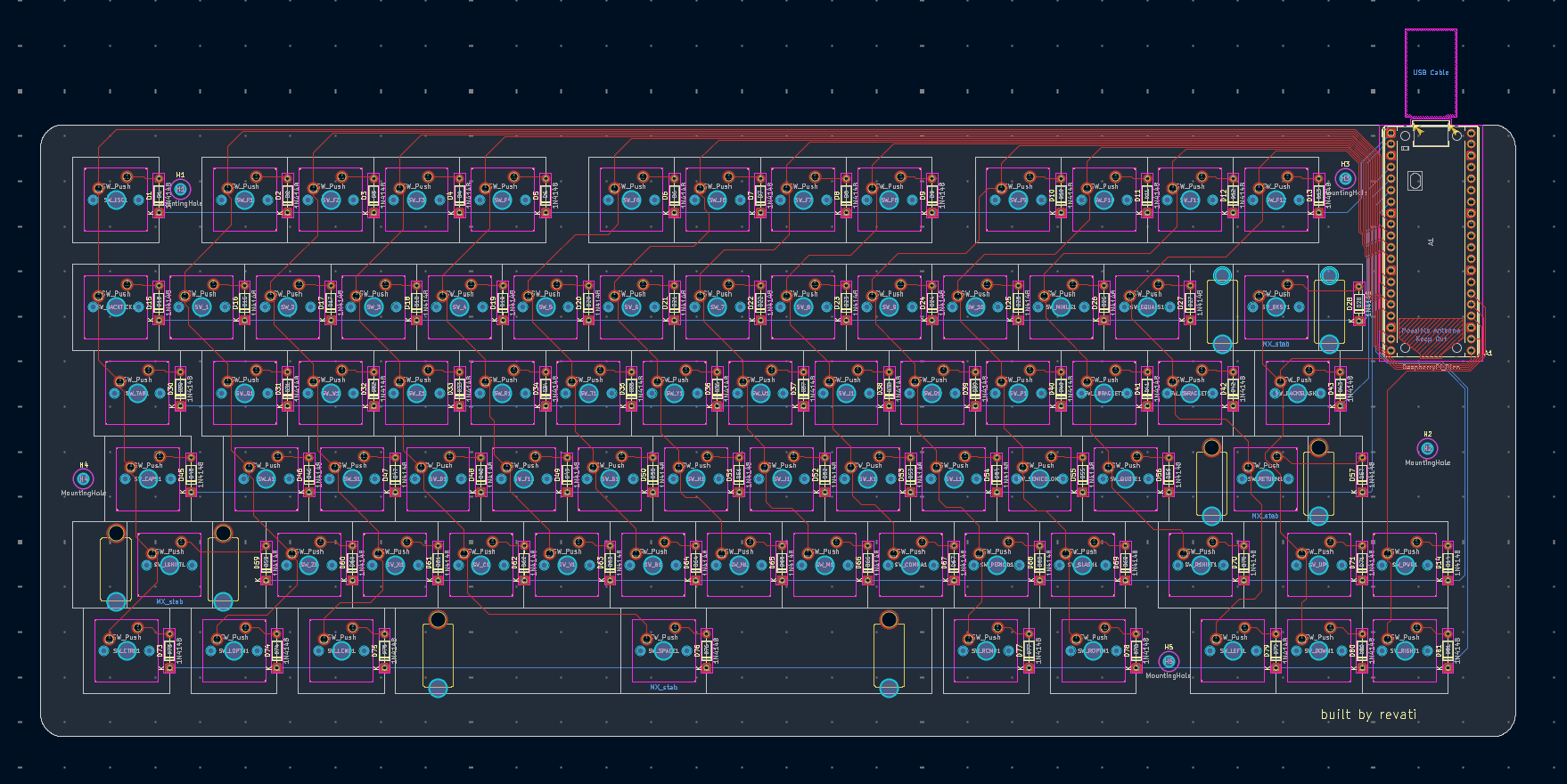
The orientation of stuff is a little ugly but I'm not too picky about how it will look as long as it functions. In the future I will most probably remake this with a different MCU that's more compact than the Pico. This is what the 3d view looks like:
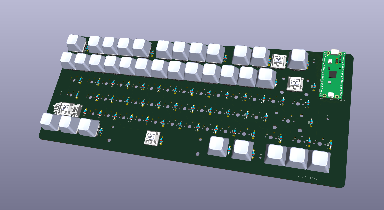
I went to GrabCAD and downloaded some 3D models of the Cherry MX keycaps and switches that were 1u. However, I got tired of adding them all in because I couldn't find a way to globally update their footprints to link to the model, so I added enough to just get an idea of what it would look like. I also added in a 1.5u stabilizer to test how that would look.
Final step for this part was running the Design Rules Checker (DRC) to make sure everything was good. I cleaned up some connections, ran the DRC again, and the PCB was ready to go! I also committed and pushed all of this to GitHub.
I realized today that I forgot to generate the drill files and gerbers and whatnot so I did that as well.
I then moved on to designing the case using Onshape. This was my first time using CAD ever, so I spent a bit acclimating to the program. I imported my PCB into the project with it's half-completed 3D models. There were enough for me to get a sense of how I should dimension my case, so it wasn't too bad.
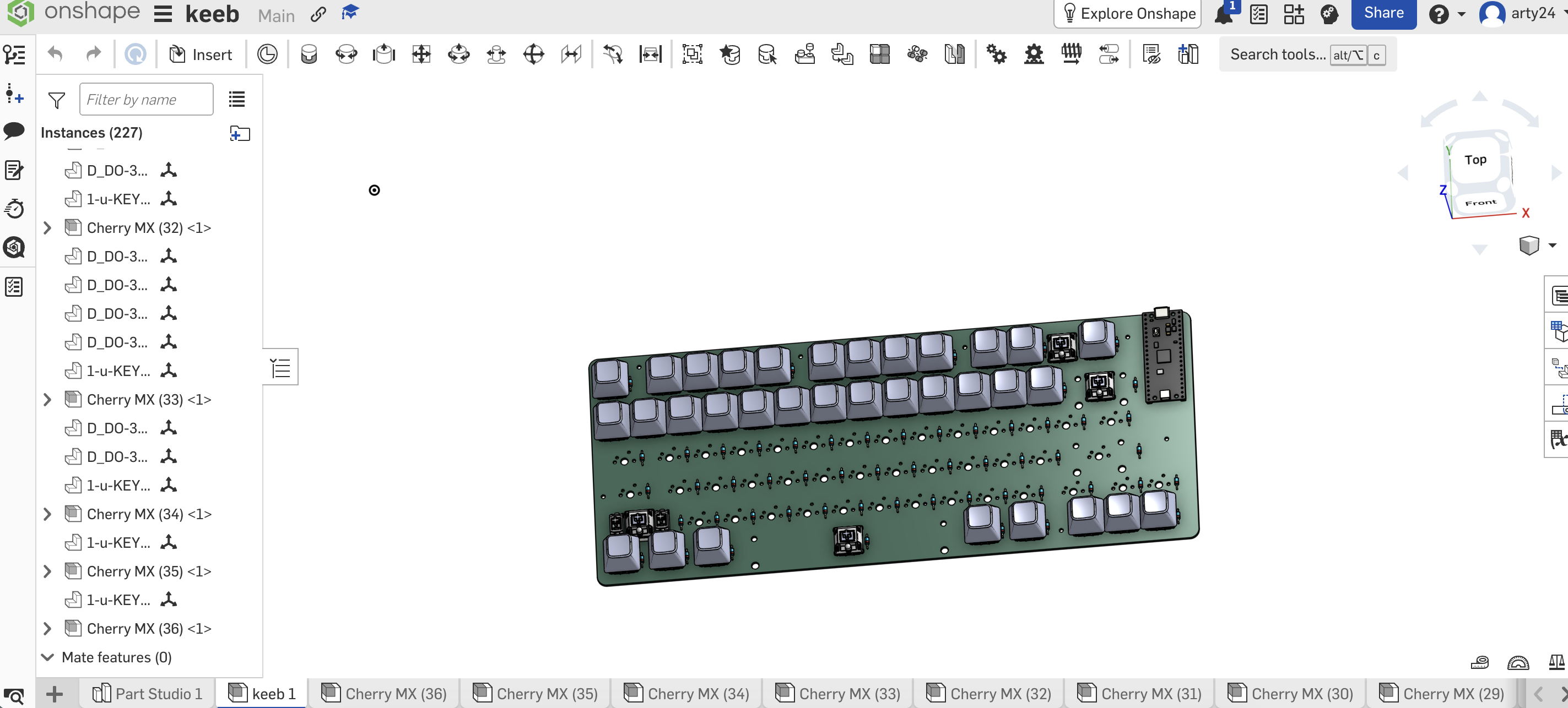
Overall I didn't get much done today.
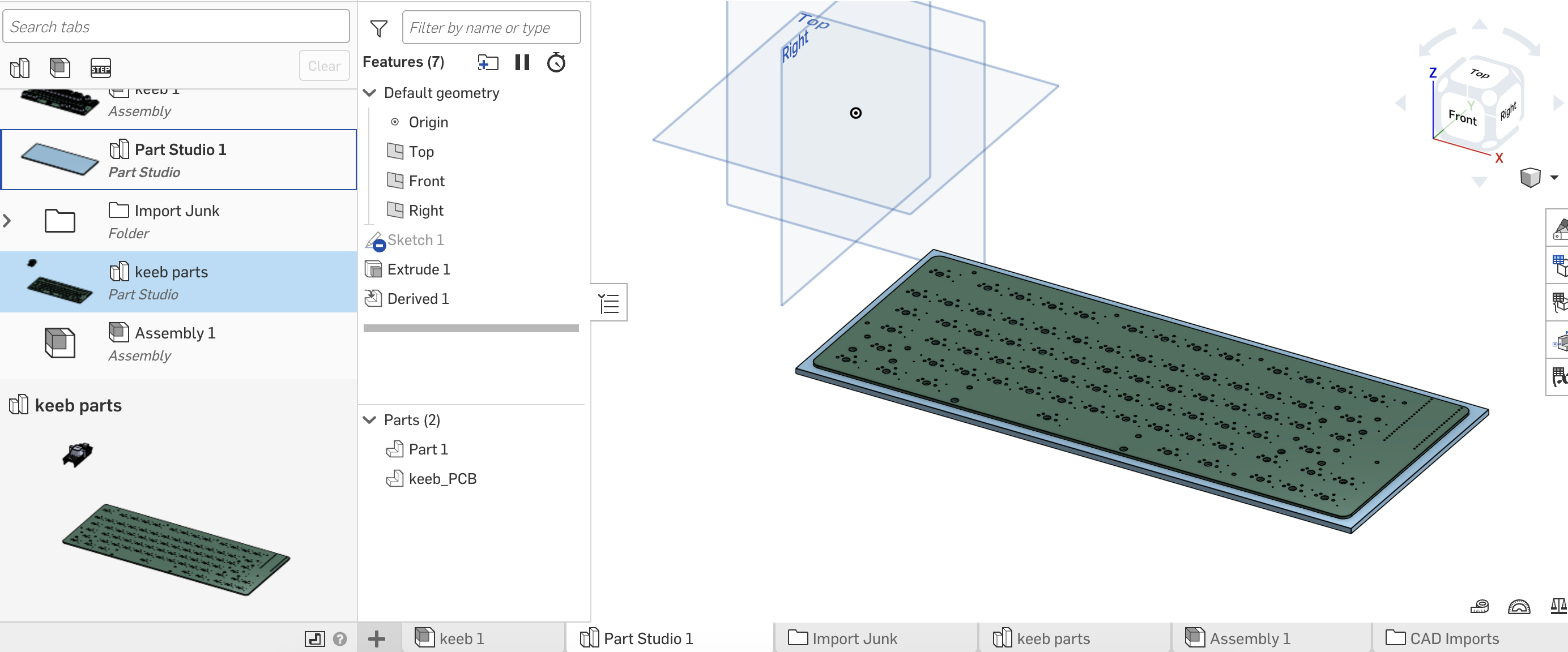
I continued working on the keyboard case. I built the base for the tray. I also struggled a lot first because i couldn't figure out how to bring the PCB over to the Parts Studio so after I figured that out this is what I had:
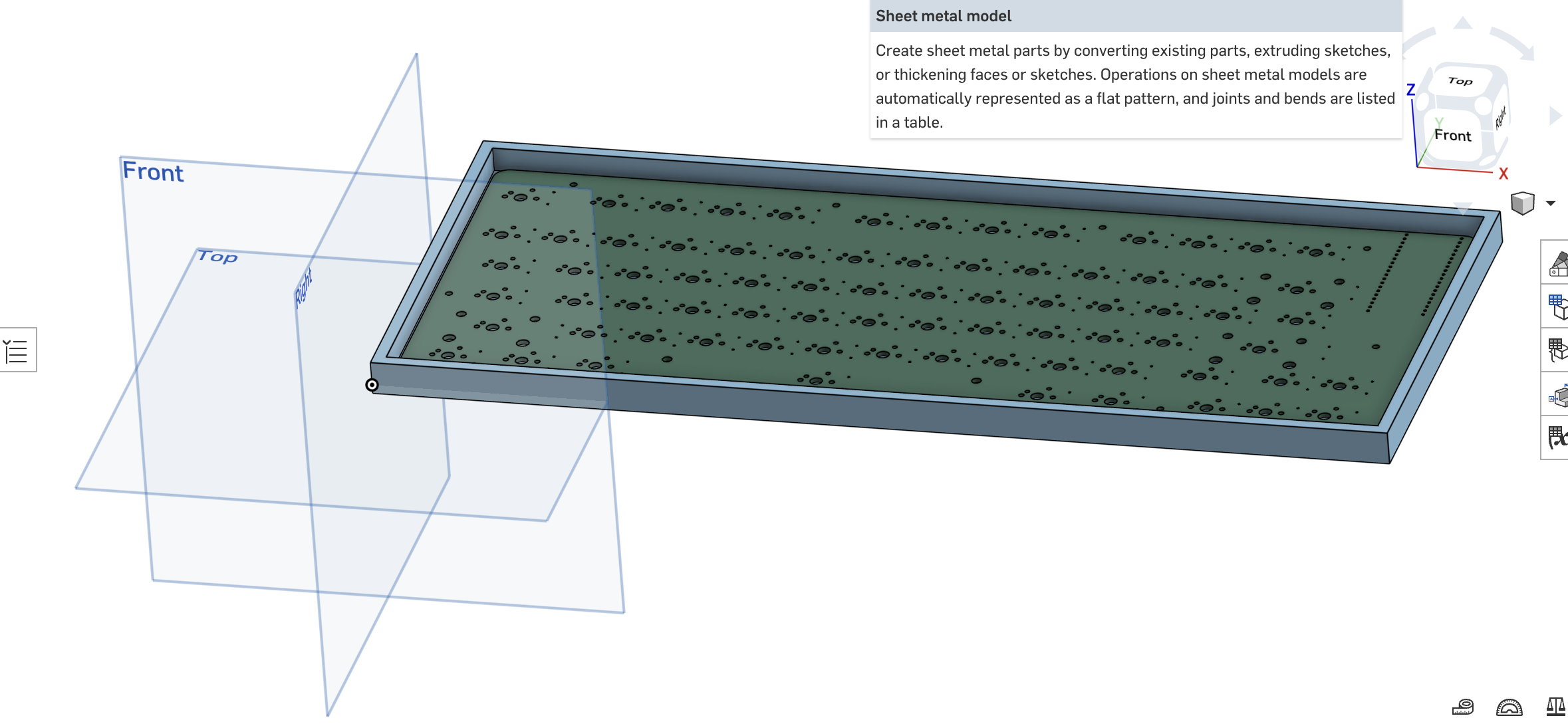
I was traveling over the weekend so I didn't work on the project much for the past couple of days. I started by creating walls around the PCB by making a new sketch. This took me around an hour ngl because I had trouble setting up my second sketch to be on top of the base I had already created. After a bunch of debugging I figured out that in CAD sketches need to be fully defined. After I made sure my base was fully defined, creating the walls was a breeze. Here's what it looks like now:
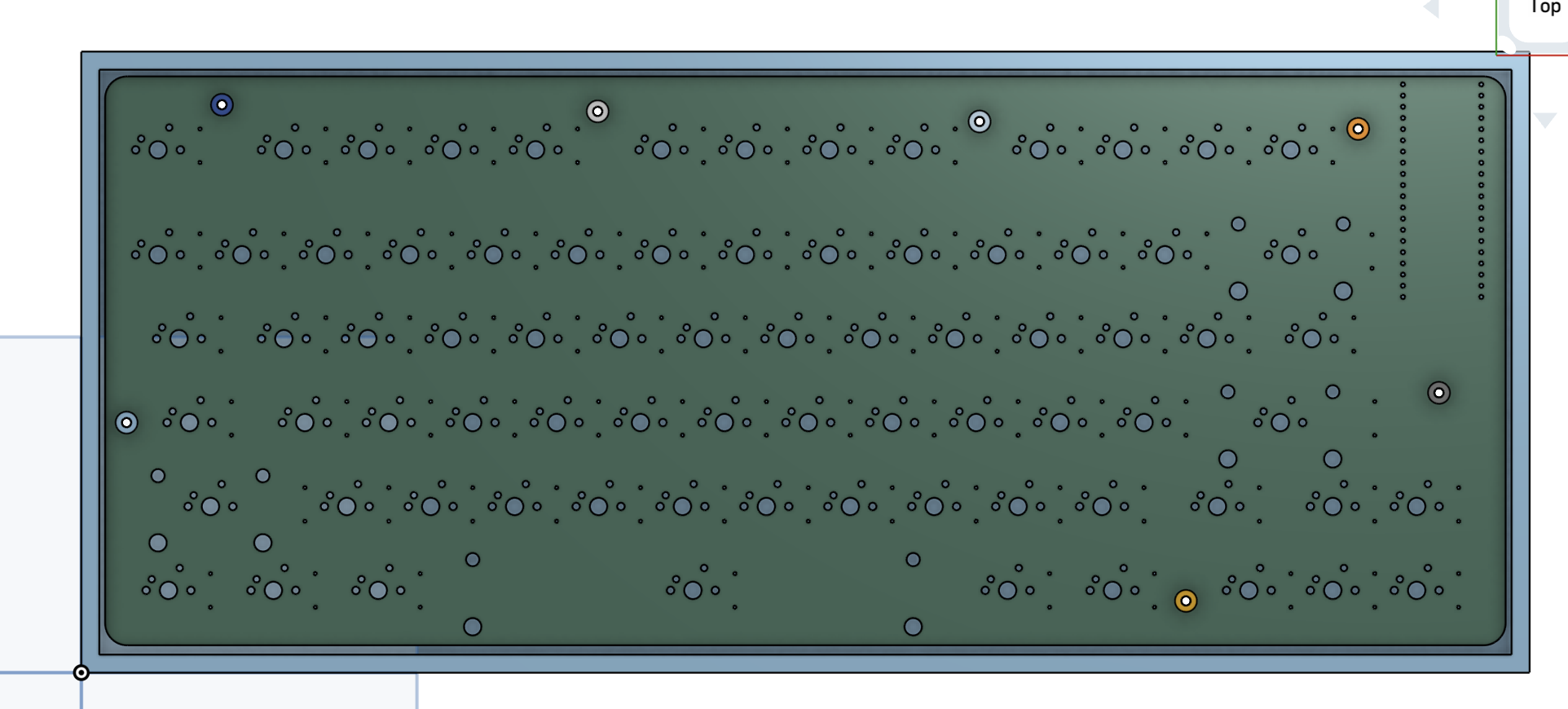
Next, I created the standoffs, which is basically a way to mount the PCB so that it fits nicely while protecting the soldered joints.
I decided against having a top plate for this first keyboard just because I don't want to mess it up initially. My plan is to instead add a top bezel if I don't like the look of just the PCB later, and print that separately. Finally I added the USB cutout and the CAD model was finished. So far, this has been my least favorite part of the process just because of how slow Onshape is on my computer. Here's the finished look:
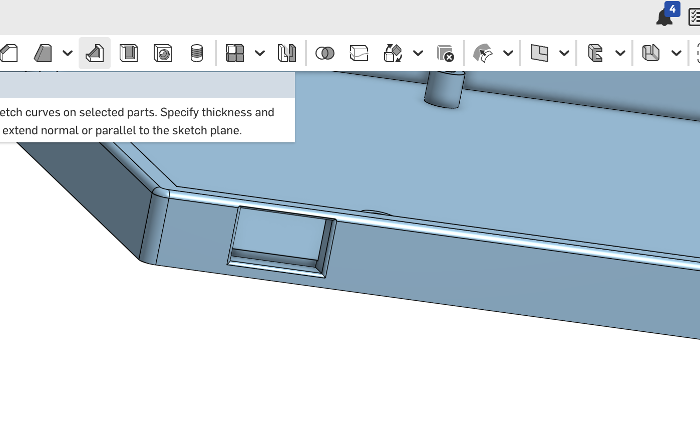
I also went ahead and split my case into two so that it would be easier to print.
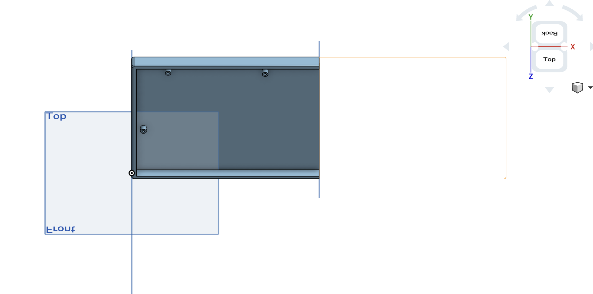
That's all I'm going to do today, I'm traveling again tomorrow so later this week I'll figure out how to use one of the slicer programs and start writing firmware.
| Qty | Value | Footprint | References |
|---|---|---|---|
| 77 | 1N4148 | Diode_THT:D_DO-35_SOD27_P7.62mm_Horizontal | D1, D2, D10, D11, D12, D13, D14, D15, D16, D17, D18, D19, D20, D21, D22, D23 +61 |
| 77 | SW_Push | PCM_marbastlib-mx:SW_MX_1u | SW_1, SW_2, SW_3, SW_4, SW_5, SW_6, SW_7, SW_8, SW_9, SW_10, SW_A1, SW_B1, SW_BACKSLASH1, SW_BACKTICK1, SW_BKSP1, SW_C1 +61 |
| 7 | MountingHole | MountingHole:MountingHole_2.2mm_M2 | H1, H2, H3, H4, H5, H6, H7 |
| 2 | MX_stab | PCM_marbastlib-mx:STAB_MX_P_2.25u | S_LSHIFT1, S_RETURN1 |
| 1 | MX_stab | PCM_marbastlib-mx:STAB_MX_P_6.25u | S_SPACE1 |
| 1 | MX_stab | PCM_marbastlib-mx:STAB_MX_2u | S_BKSP1 |
| 1 | RaspberryPi_Pico | Module:RaspberryPi_Pico_Common_THT | A1 |
It measures 317.9 × 129.1 mm and has 2 copper layers, 1.6 mm thick.
166 parts. The full list of its parts is on this page, with links to each part's symbol and footprint where PCBKit's library has them.
From the djarty24/keeb repository on GitHub, at the commit this page was made from: the board is keeb.kicad_pcb and its schematic keeb.kicad_sch. PCBKit opens the board in the browser, with nothing to install.
Its repository states no licence, so its author keeps all rights: ask djarty24 before reusing the design.


schlae/HardDriveInfo
Repair info and schematics for mostly older MFM hard drives

Thorinair/Avalon-Harmonics
A collection of Avalon Harmonics branded synthesizer modules.

doppelhub/Honda_Insight_LiBCM
Replacement BCM for G1 Honda Insight Lithium Conversion

OpenLogicEFI/Hardware
Hardware is based off an open source project called Speeduino by Josh Stewart.
