2 layers90 × 76.5 mm

 dish-glitch/Microgrid-Home-Energy-Monitor1
I want to understand how power is measured, how the grid sees demand so I will try to build a custom PCB that clips non-invasive current transformer sensors around wires and measure real-time power usage I would like it to measure Watts. Apparent power (VA) and Power factor.
Microgrid Home Energy Monitor is an open-source printed circuit board by dish-glitch, from the dish-glitch/Microgrid-Home-Energy-Monitor repository on GitHub, published under the MIT licence. It is a 2-layer board of 130.2 × 72.9 mm with 41 parts on 55 nets, routed with 332 tracks and 34 vias.
It is built around the ESP32-WROOM-32 and AMS1117-3.3. Its parts include 14 resistors, 9 capacitors, 6 connectors, 3 ICs and 2 diodes. It belongs with the sensors and measurement boards and the ESP32 boards of this library.


Custom 2-layer PCB designed in KiCad 9. Measures real-time household power consumption using non-invasive current transformer sensors.
| Spec | Value |
|---|---|
| Layers | 2 (F.Cu / B.Cu) |
| Board dimensions | ~130mm × 75mm |
| Min trace width | 0.2mm signal / 0.4mm power |
| Min clearance | 0.15mm (accommodates the USB-C footprint's pad spacing; JLCPCB handles down to 0.127mm) |
| Copper pour | GND flood on F.Cu + solid GND plane on B.Cu, joined by stitching vias |
| Via drill | 0.3mm min |
| Surface finish | HASL (lead-free) |
| Fabrication | JLCPCB |
USB-C (5V VBUS) → AMS1117-3.3 linear regulator → 3.3V rail → ESP32 + all peripherals
CC1 and CC2 resistors (5.1kΩ to GND) identify the board as a USB device to the host charger, enabling 5V/500mA delivery per USB-C spec.
Each channel processes the AC output of an SCT-013-000 current transformer:
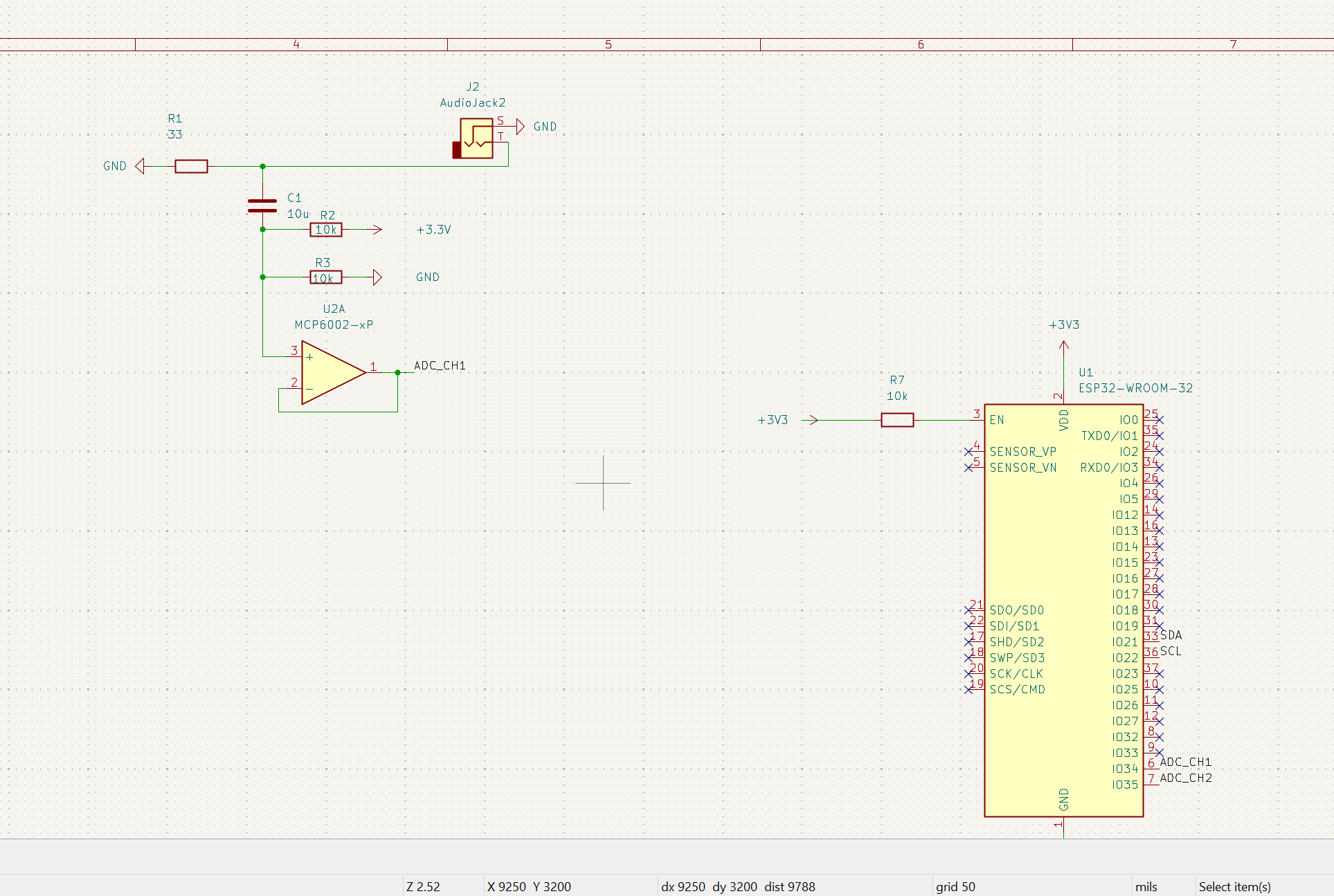
SCT-013 → 33Ω burden resistor → 10µF coupling cap → MCP6002 op-amp buffer → ESP32 ADC
                                    ↑
                          10kΩ/10kΩ bias divider (1.65V midpoint)
Burden resistor (33Ω): The SCT-013 outputs a small currecnt but the ESP32 measures the voltage. The 33 ohm burden resisotr converts that currecnt into a voltage using Ohm's law. At the senors's max rated current, this produeces 1.65 V RMS 2.33 V peak.
Bias divider (2× 10kΩ): Becuase the ESP32 ADC can't read negative voltages, 2 10k ohm resistors create a 1.65 V bais point.
Coupling capacitor (10µF): Blocks DC from the burden resistor, and passes the 60Hz AC signal.
MCP6002 buffer: Unity-gain op-amp buffer to keep the bais network independent from the ESP32 ADC. Its high imput impedance prevents the bais voltage from shifting.
ZMPT101B voltage transformer connects to J6. its output is routed to GPIO36 which is an input-only ADC pin with no internal pull resistors, chosen to minimize noise on the analog signal.
SDA (GPIO21) and SCL (GPIO22) pulled up to 3.3V via 4.7kΩ resistors. Pull-up value chosen for standard-mode I2C (100 kHz) with expected bus capacitance under 50pF.
See Microgrid-Home-Energy-Monitor.kicad_sch
See Microgrid-Home-Energy-Monitor.kicad_pcb
Key layout decisions:
| Ref | Component | Value | Package | MPN | Supplier |
|---|---|---|---|---|---|
| U1 | ESP32-WROOM-32 | — | Module | ESP32-WROOM-32E-N4 | Mouser 356-ESP32WROOM32EN4 |
| U2 | MCP6002 Op-Amp | — | DIP-8 | MCP6002-I/P | Digikey MCP6002-I/P-ND |
| U3 | AMS1117-3.3 | 3.3V LDO | SOT-223 | AMS1117-3.3 | Digikey 1665-1016-1-ND |
| J1, J2 | CT Sensor Input | 3.5mm jack | SMD | SJ-3523-SMT | Digikey CP-3523SJCT-ND |
| J3 | OLED Connector | 4-pin | 2.54mm header | — | generic |
| J4 | USB-C Receptacle (optional, see notes) | USB 2.0 | THT 16P | GCT USB4085-GF-A | Digikey 2073-USB4085-GF-ACT-ND |
| J5 | Programming Header | 6-pin | 2.54mm header | — | generic |
| J6 | ZMPT101B Connector | 3-pin | 2.54mm header | — | generic |
| R1, R4 | Burden Resistor (CH1, CH2) | 33Ω 1% | 0603 | — | generic |
| R2, R3, R5, R6 | Bias Resistor (R2/R3 CH1, R5/R6 CH2) | 10kΩ | 0603 | — | generic |
| R7 | EN Pull-up | 10kΩ | 0603 | — | generic |
| R8, R9 | I2C Pull-up | 4.7kΩ | 0603 | — | generic |
| R10 | GPIO0 Pull-up — do not fit on rev 1, see notes | 10kΩ | 0603 | — | generic |
| R11, R12 | CC Pull-down (only needed with J4) | 5.1kΩ | 0603 | — | generic |
| R13, R14 | LED Current Limit | 150Ω | 0603 | — | generic |
| C1, C2 | Coupling Cap | 10µF | 0805 | — | generic |
| C3, C6 | LDO Bulk Cap | 10µF | 0805 | — | generic |
| C4, C5 | LDO Bypass Cap | 100nF | 0603 | — | generic |
| C7 | ESP32 Bypass | 100nF | 0603 | — | generic |
| C8 | ESP32 Bulk | 10µF | 0805 | — | generic |
| C9 | EN Filter Cap | 100nF | 0603 | — | generic |
| D1 | Power LED | Red | 3mm THT | — | generic |
| D2 | Status LED | Green | 3mm THT | — | generic |
| SW1 | Reset Button | — | 6mm THT | — | generic |
| SW2 | Boot Button | — | 6mm THT | — | generic |
| CT1, CT2 | CT Sensor | SCT-013-000 | Clamp | SCT-013-000 | Amazon/AliExpress |
| VT1 | Voltage Sensor Module (plugs into J6) | ZMPT101B | Module | ZMPT101B | Amazon/AliExpress |
Lessons from assembling the first board (solder paste + hot plate for SMD, iron for THT):
01C (EIA-96) or 103. A part marked 01X is 10Ω — fitting those in R2/R3/R5/R6 puts two 20Ω paths across the 3.3V rail and looks exactly like a short (supply drops into CC, the resistors near U2 get warm).PIN_CT1, real power + PF), J1 feeds R4/C2 → GPIO35 (PIN_CT2). Plug the clamp for the main load into J2.| Check | Expected |
|---|---|
| TP2 (3.3V) ↔ TP3 (GND), continuity, unpowered | No beep |
| 5V supply, ESP32 with factory firmware | CV, ~0.11 A, D1 lit |
| TP2 | 3.3V |
board-test sketch, no sensors connected | CT1 ≈ CT2 ≈ 1650 mV (bias midpoint), D2 blinking, BOOT button reported |
| OLED on J3 | I2C scan finds 0x3C |
All fixes from the 2026-07-02 DRC audit are complete (verified with kicad-cli):
Gerber files for JLCPCB are in gerbers/ — exported from the DRC-clean board, ready to upload.
JLCPCB order settings:
| Qty | Value | Footprint | References |
|---|---|---|---|
| 6 | 10k | Resistor_SMD:R_0603_1608Metric | R2, R3, R5, R6, R7, R10 |
| 5 | TestPoint | TestPoint:TestPoint_Pad_D1.5mm | TP1, TP2, TP3, TP4, TP5 |
| 3 | 100nF | Capacitor_SMD:C_0603_1608Metric | C4, C5, C9 |
| 3 | 10u | Capacitor_SMD:C_0805_2012Metric | C1, C2, C8 |
| 2 | 10uF | Capacitor_SMD:C_0805_2012Metric | C3, C6 |
| 2 | 150 | Resistor_SMD:R_0603_1608Metric | R13, R14 |
| 2 | 33 | Resistor_SMD:R_0603_1608Metric | R1, R4 |
| 2 | 4.7k | Resistor_SMD:R_0603_1608Metric | R8, R9 |
| 2 | 5.1k | Resistor_SMD:R_0603_1608Metric | R11, R12 |
| 2 | AudioJack2 | Connector_Audio:Jack_3.5mm_CUI_SJ-3523-SMT_Horizontal | J1, J2 |
| 2 | LED | LED_THT:LED_D3.0mm | D1, D2 |
| 2 | SW_Push | Button_Switch_THT:SW_PUSH_6mm_H4.3mm | SW1, SW2 |
| 1 | 0.1u | Capacitor_SMD:C_0603_1608Metric | C7 |
| 1 | AMS1117-3.3 | Package_TO_SOT_SMD:SOT-223-3_TabPin2 | U3 |
| 1 | Conn_01x03 | Connector_PinHeader_2.54mm:PinHeader_1x03_P2.54mm_Vertical | J6 |
| 1 | Conn_01x04 | Connector_PinHeader_2.54mm:PinHeader_1x04_P2.54mm_Vertical | J3 |
| 1 | Conn_01x06 | Connector_PinHeader_2.54mm:PinHeader_1x06_P2.54mm_Vertical | J5 |
| 1 | ESP32-WROOM-32 | RF_Module:ESP32-WROOM-32 | U1 |
| 1 | MCP6002-xP | Package_DIP:DIP-8_W7.62mm | U2 |
| 1 | USB_C_Receptacle_USB2.0_16P | Connector_USB:USB_C_Receptacle_GCT_USB4085 | J4 |


Hasenpups/WLED_ESP32_Controller
This work is licensed under a [Creative Commons Attribution-NonCommercial-ShareAlike 4.0 International License][cc-by-nc-sa].


nuclearcat/ESP32ETH
Simple ESP32 with native ethernet using LAN8720 phy, Arduino compatible

larryqiann/AP1512HH-ESP32
Coway AP1512HH Main Board replacement with ESP32


It measures 130.2 × 72.9 mm and has 2 copper layers, 1.6 mm thick.
41 parts, built around the ESP32-WROOM-32 and AMS1117-3.3. The full list of its parts is on this page, with links to each part's symbol and footprint where PCBKit's library has them.
From the dish-glitch/Microgrid-Home-Energy-Monitor repository on GitHub, at the commit this page was made from: the board is hardware/Microgrid-Home-Energy-Monitor.kicad_pcb and its schematic hardware/Microgrid-Home-Energy-Monitor.kicad_sch. PCBKit opens the board in the browser, with nothing to install.
Its repository publishes it under the MIT licence: you may reuse it on that licence's terms (keep the author's notice, and for a copyleft licence share your changes alike).