2 layers76.5 × 120 mm
Numpad project
hackclub/OnBoard
💡 Join 1,000 teenagers and make your first PCB with a $100 grant!
64 parts915

 Disasm/hc245t-bypass26
This tiny board is useful to replace 74HC245T chips on Colorlight 5A-75B and 5A-75E boards.
Hc245t bypass panel is an open-source printed circuit board by Disasm, from the Disasm/hc245t-bypass repository on GitHub. It is a 2-layer board of 14.2 × 13 mm with 64 parts on 8 nets, routed with 196 tracks and 52 vias.
hc245t-bypassThis tiny board is useful to replace 74HC245T chips on Colorlight 5A-75B and 5A-75E boards.
You can order these boards from OSH Park: https://oshpark.com/shared_projects/Og8YtGBU Don't forget to select Flex board type on the order page!
The board needs some rework to improve solderability. It's also possible to solder it "as is", but you can encounter shorts between the adjacent pins.
First, separate the boards from a panel. This can be done easily with scissors.
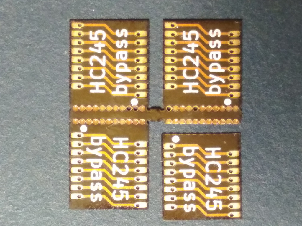
Next, cut each board by the line marked in red. The line should be on the edge of each via, not on the center. Try to make the line as straight as possible. The idea is to cut as much copper as possible, avoiding cutting most of the via copper.
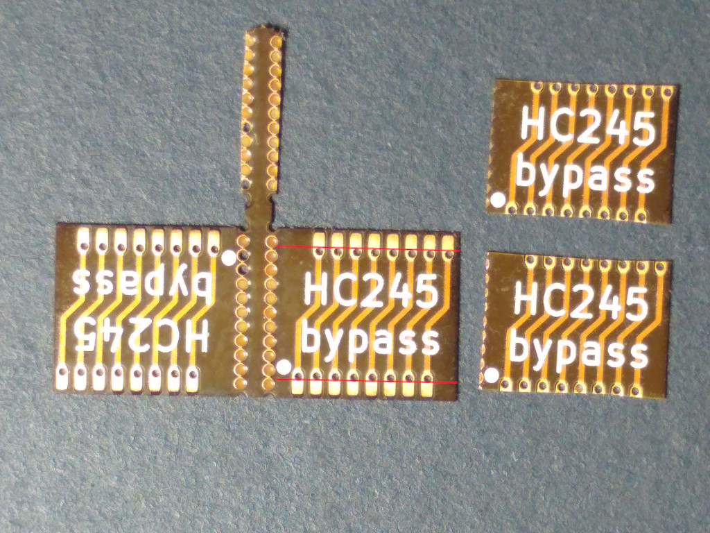
Now solder it! Note that the first "pin" on the flex board corresponds to the second pin of the 74HC245T footpint.
You can also skip soldering about 50% of 74HC245T footprints by skipping footprints that are used for common signal (like A-E, CLK, LATCH, BLANK) distribution. You can learn in advance which footprints you need to solder and which not. Usually "color" signals are distributed through separate 74HC245T buffers located in groups of 3. Of course, this way you will not be able to control 8 signals out of... many, but it's still a good price for not soldering ~50% of tiny boards.
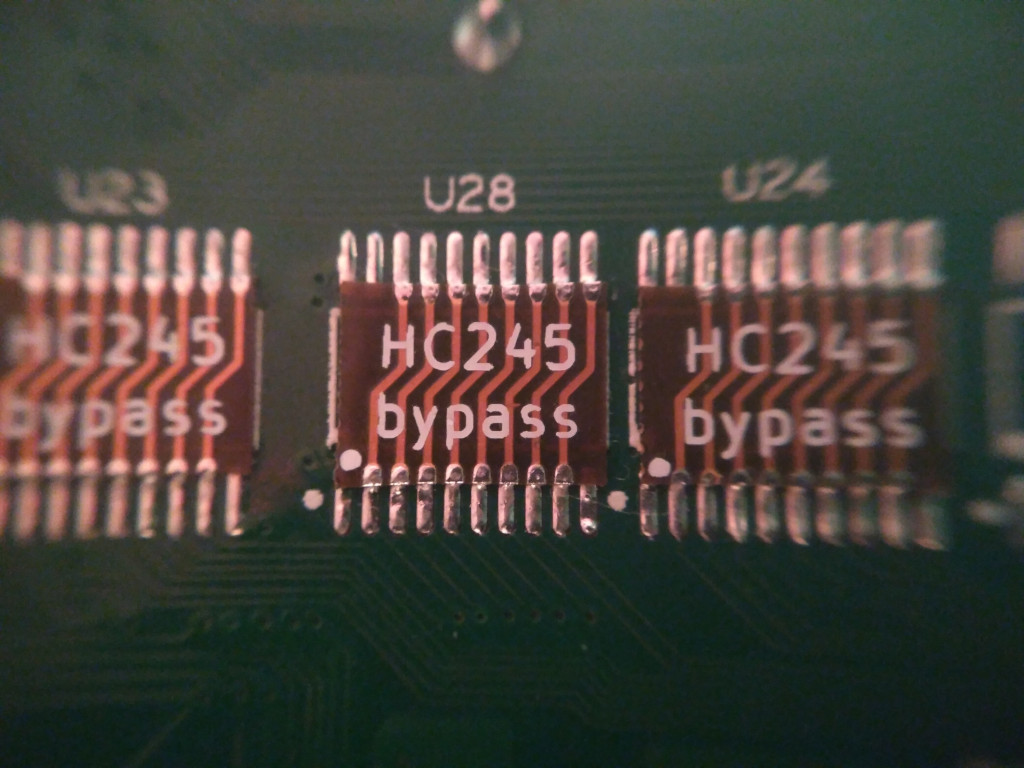
Additionally, you can use a continuity tester to check that all "data" pins are connected and adjacent pins are not shorted accidentally. Some of the 74HC245T footpints used for common signal distribution have some of the pins connected together. Check twice: probably your "ringing" footprint has some signals connected on purpose.
Shoutouts to Tom Keddie, who made the first prototype with OSH Park flex board process. Unfortunately, castellated vias on OSH Park flex boards are not officially supported, and they do not guarantee correct manufacturing for such vias. The board in this repo is the improved version of the prototype with the following changes:
| Qty | Value | Footprint | References |
|---|---|---|---|
| 64 | TestPoint | hc245t-bypass:PAD | TP1, TP1, TP1, TP1, TP10, TP10, TP10, TP10, TP11, TP11, TP11, TP11, TP12, TP12, TP12, TP12 +48 |
It measures 14.2 × 13 mm and has 2 copper layers, 1.6 mm thick.
64 parts. The full list of its parts is on this page, with links to each part's symbol and footprint where PCBKit's library has them.
From the Disasm/hc245t-bypass repository on GitHub, at the commit this page was made from: the board is hc245t-bypass-panel.kicad_pcb. PCBKit opens the board in the browser, with nothing to install.
Its repository states no licence, so its author keeps all rights: ask Disasm before reusing the design.
hackclub/OnBoard
💡 Join 1,000 teenagers and make your first PCB with a $100 grant!

drandyhaas/KiCadRoutingTools
A set of Python/Rust tools to aid routing in KiCad

BlueSCSI/BlueSCSI-v2
BlueSCSI v2/Ultra - an open source, open hardware, SCSI emulator using the Pi Pico PR2040 and Pico 2 RP2350


PyrooL/Alpha
A 28-key semi-ortholinear mechanical keyboard designed by PyroL

ugcs/ddc
Drone Show Software is software designed for drone shows, allowing flight path planning as well as control of dozens of drones simultaneously in a synchronized manner.
