2 layers40 × 30 mm
 diodeinc/example1
Zener Example repo
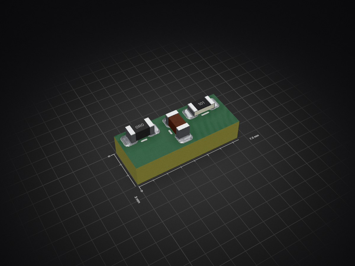
MatchingNetwork is an open-source printed circuit board by diodeinc, from the diodeinc/example repository on GitHub. It is a 2-layer board with 3 parts on 4 nets.
Its parts include 1 capacitor, 1 resistor and 1 inductor.
This repo demonstrates designing PCBs with the Zener language (.zen) and the open-source pcb compiler. You describe parts and connectivity in .zen, compose them into boards, and generate KiCad projects for layout/manufacturing.
To recreate this example step by step, visit the tutorial
For the most up to date information, visit our documentation at docs.pcb.new
The open source PCB compiler is available at github.com/diodeinc/pcb
.
├── README.md
├── components              # Physical items on the PCB that usually don't have an existing generic
├── modules                 # Reusable pieces of Zener that can be composed of one or more components or other modules
├── boards                  # Board compositions (.zen)
└── pcb.toml # Workspace + dependenciesComponent(...): Defines a part by symbol/footprint and pinsio(...): Declares typed ports/nets (e.g., Net, Ground)Module("path"): Reuses another .zen moduleLayout(...): Hints where to emit previews/outputsSee modules/Antenna.zen, modules/SMAConnector.zen, and the composed board boards/EX0001/EX0001.zen for examples.
pcb compiler and KiCad 9 (see docs link above)modules/ and the board in boards/EX0001/EX0001.zen.zen, to generate outputs (KiCad project, previews, docs). Refer to the docs for exact commands on your platformNotes:
pcb.toml declares the workspace and pulls the Zener stdlibboards/EX0001/docs/spec.md.zen| Qty | Value | Footprint | References |
|---|---|---|---|
| 1 | 100 | R_0603_1608Metric:R_0603_1608Metric | R1 |
| 1 | 10nH | L_0603_1608Metric:L_0603_1608Metric | L1 |
| 1 | 10pF | C_0603_1608Metric:C_0603_1608Metric | C1 |
3 parts. The full list of its parts is on this page, with links to each part's symbol and footprint where PCBKit's library has them.
From the diodeinc/example repository on GitHub, at the commit this page was made from: the board is modules/layout/MatchingNetwork/layout.kicad_pcb. PCBKit opens the board in the browser, with nothing to install.
Its repository states no licence, so its author keeps all rights: ask diodeinc before reusing the design.

hzeller/rpi-rgb-led-matrix
Controlling up to three chains of 64x64, 32x32, 16x32 or similar RGB LED displays using Raspberry Pi GPIO


atopile/atopile
Design circuit boards with code! ✨ Get software-like design reuse 🚀, validation, version control and collaboration in hardware; starting with electronics ⚡️


hackclub/sprig
🍃 Learn to code by making games in a JavaScript web-based game editor.