
2 layers327.9 × 139 mm
Coco2
baldengineer/bit-preserve
Project for capturing vintage, classic, aka old computer schematics in KiCad.
147 parts446

 dillyshan/555-timer-pcb
A 555 timer PCB designed in KiCad.
555-timer pcb is an open-source printed circuit board by dillyshan, from the dillyshan/555-timer-pcb repository on GitHub. It is a 2-layer board of 50 × 40 mm with 9 parts on 7 nets, routed with 26 tracks and 0 vias.
It is built around the NE555P. Its parts include 3 capacitors, 3 resistors, 1 IC, 1 diode and 1 connector.
A 555 timer PCB designed in KiCad.
This is my first PCB design project, created to learn the complete PCB design workflow using KiCad. The circuit uses an NE555 timer in astable mode to generate a repeating output signal that drives an LED.
The project covers schematic design, footprint assignment, PCB layout, component placement, routing, ground planes, ERC/DRC verification, and manufacturing file generation.
The NE555 timer is configured in astable mode, meaning it continuously switches between HIGH and LOW without requiring an external trigger. R1, R2, and C1 control the timing of the oscillation.
As C1 repeatedly charges and discharges, the NE555 output at pin 3 switches between HIGH and LOW. The output drives the LED through R3, causing the LED to blink.
C2 and C3 are used for stability and noise filtering.
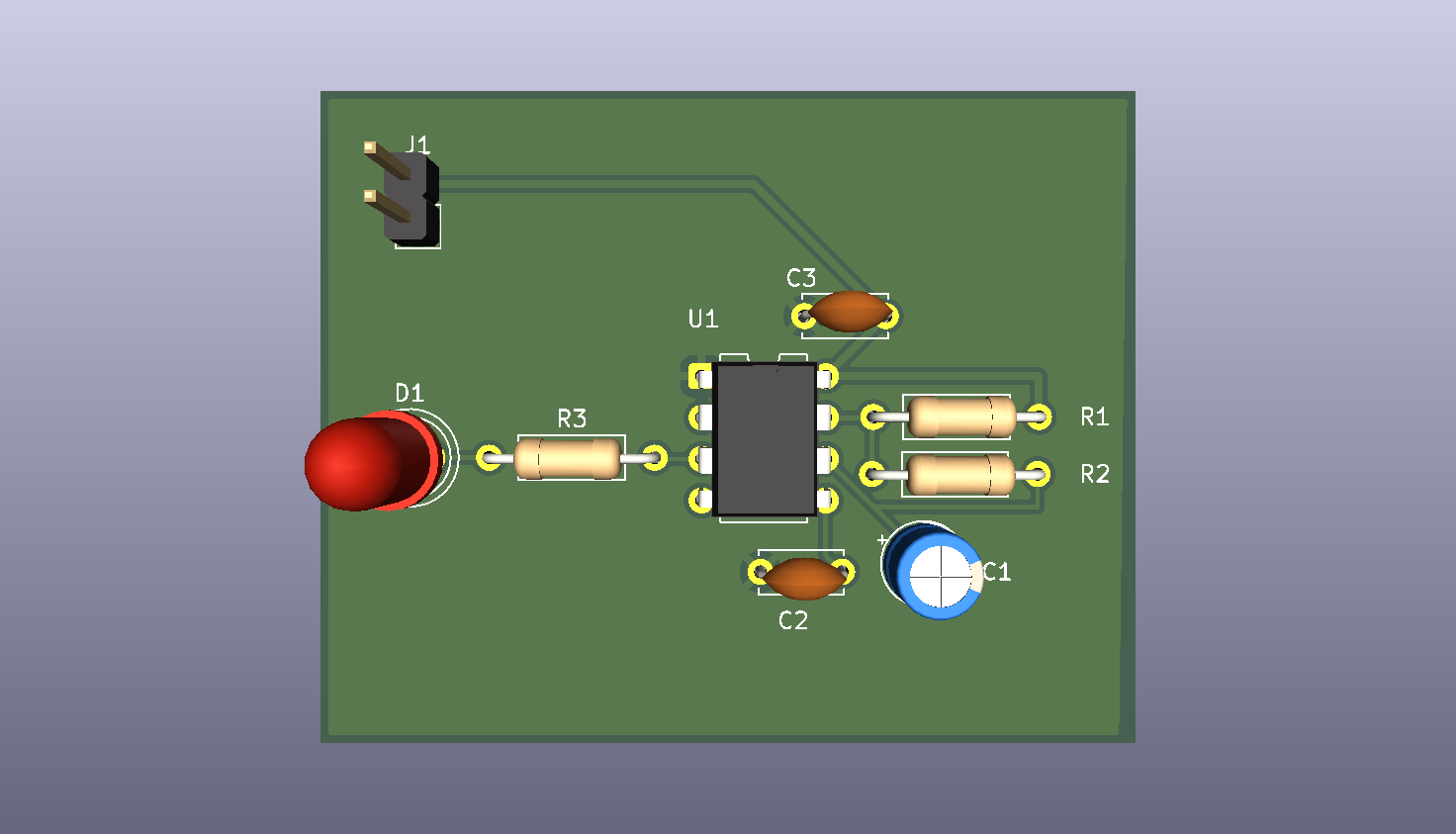
Through this project, I learned how to:
| Qty | Value | Footprint | References |
|---|---|---|---|
| 1 | 100k | Resistor_THT:R_Axial_DIN0207_L6.3mm_D2.5mm_P10.16mm_Horizontal | R2 |
| 1 | 100nF | Capacitor_THT:C_Disc_D5.0mm_W2.5mm_P5.00mm | C3 |
| 1 | 10k | Resistor_THT:R_Axial_DIN0207_L6.3mm_D2.5mm_P10.16mm_Horizontal | R1 |
| 1 | 10nF | Capacitor_THT:C_Disc_D5.0mm_W2.5mm_P5.00mm | C2 |
| 1 | 10μF | Capacitor_THT:CP_Radial_D5.0mm_P2.00mm | C1 |
| 1 | 1k | Resistor_THT:R_Axial_DIN0207_L6.3mm_D2.5mm_P10.16mm_Horizontal | R3 |
| 1 | Conn_01x02 | Connector_PinHeader_2.54mm:PinHeader_1x02_P2.54mm_Vertical | J1 |
| 1 | LED | LED_THT:LED_D5.0mm | D1 |
| 1 | NE555P | Package_DIP:DIP-8_W7.62mm | U1 |
It measures 50 × 40 mm and has 2 copper layers, 1.6 mm thick.
9 parts, built around the NE555P. The full list of its parts is on this page, with links to each part's symbol and footprint where PCBKit's library has them.
From the dillyshan/555-timer-pcb repository on GitHub, at the commit this page was made from: the board is 555_Timer_PCB.kicad_pcb and its schematic 555_Timer_PCB.kicad_sch. PCBKit opens the board in the browser, with nothing to install.
Its repository states no licence, so its author keeps all rights: ask dillyshan before reusing the design.
baldengineer/bit-preserve
Project for capturing vintage, classic, aka old computer schematics in KiCad.

The-Invent0r/8-bit-Computer-PCB
These are the KiCAD files for my 8-Bit Computer.

DarcyJProjects/touchtone555
An open-source DIY, NE555-based analogue synthesizer - play notes with a stylus


benjiaomodular/SynthCard
I designed this project with the help of PCBWay. You can get a copy of these cards through the PCBWay Shared Projects page.

fortinsylvain/MyCpu
Home brew CPU Hardware with 1-bit ALU implementation using 74LSxx, a micro-code and assembler coded in C#.

hackup/C128Diag
Replica of the Commodore C128 Diagnostic Test cartridge Assy No. 325093-01.