2 layers100 × 64.9 mm

 dhanush-darpan/Smart-Home-Automation-Controller-PCB
This repository contains the KiCad project files, PCB layout, schematic, and a printable PDF of the board for the Smart Home Automation Controller.
Smart home automation controller is an open-source printed circuit board by dhanush-darpan, from the dhanush-darpan/Smart-Home-Automation-Controller-PCB repository on GitHub. It is a 2-layer board of 168 × 61 mm with 72 parts on 92 nets, routed with 553 tracks and 37 vias.
It is built around the ATMEGA328P-PU, ESP-WROOM-02 and TXS0101DBV, with the MMBTA06 among its other parts. Its parts include 20 resistors, 14 diodes, 10 ICs, 8 connectors and 8 switches. It belongs with the home automation and IoT boards and the AVR (ATmega, ATtiny) boards of this library.


KiCad project — PCB design for a Smart Home Automation Controller.
This repository contains the KiCad project files, PCB layout, schematic, and a printable PDF of the board for the Smart Home Automation Controller. The design includes relay driver circuits and Wi‑Fi communication components (see schematic for detailed parts and net connections).
This README explains the project structure, how to open and build the board in KiCad, fabrication export steps, and housekeeping notes for contributors.
Files included in the repo:
smart_home_automation_controller.kicad_pcb — PCB layout file.smart_home_automation_controller.kicad_sch — KiCad schematic file.smart_home_automation_controller.kicad_pro — KiCad project file (project metadata).smart_home_automation_controller.kicad_prl — Project resource/library file (local machine/paths).smart_home_automation_controller.pdf — Printable/exported PDF of the PCB (for quick review/printing).Keep the following in the repo since they are needed to reproduce and edit the project:
*.kicad_sch — schematic sources.*.kicad_pcb — PCB layout.*.kicad_pro — project metadata (useful for collaborators).*.pdf (optional) — board print or notes (only include if you want a quick preview in the repo).*.kicad_pro file in the project root.kicad-cli tools (or a script) to export a CSV/BOM. Verify component footprints, values, and manufacturer part numbers before ordering.BOM/ folder if you want to track part numbers and costs as the project matures.(Adjust the above to match your intended manufacturing choices.)
This repository serves as a complete reference for designing, maintaining, and fabricating a Smart Home Automation Controller PCB using KiCad. By following the provided guidelines for file management, version control, and project documentation, collaborators and manufacturers can efficiently reproduce the design. Proper use of .gitignore, BOM tracking, and GitHub Releases ensures the project remains clean, scalable, and useful for future iterations or community contributions.
| Qty | Value | Footprint | References |
|---|---|---|---|
| 8 | 680E | Resistor_SMD:R_0201_0603Metric | R7, R8, R9, R10, R11, R12, R13, R14 |
| 8 | LED | LED_SMD:LED_0201_0603Metric | D7, D8, D9, D10, D11, D12, D13, D14 |
| 6 | 1K | Resistor_SMD:R_0201_0603Metric | R1, R2, R3, R4, R5, R6 |
| 6 | 1N4007 | Diode_SMD:D_1206_3216Metric | D1, D2, D3, D4, D5, D6 |
| 6 | 220E | Resistor_SMD:R_0201_0603Metric | R15, R16, R17, R18, R19, R20 |
| 6 | G5LE-1 | Relay_THT:Relay_SPDT_Omron-G5LE-1 | K1, K2, K3, K4, K5, K6 |
| 6 | MMBTA06 | Package_TO_SOT_SMD:SOT-23 | Q1, Q2, Q3, Q4, Q5, Q6 |
| 6 | NC COM NO | Connector_JST:JST_NV_B03P-NV_1x03_P5.00mm_Vertical | J1, J2, J3, J4, J5, J6 |
| 6 | PC817 | Package_DIP:DIP-4_W7.62mm | U5, U6, U7, U8, U9, U10 |
| 4 | MountingHole_Pad | MountingHole:MountingHole_2.2mm_M2_DIN965_Pad | H1, H2, H3, H4 |
| 2 | 100nF | Capacitor_SMD:C_0201_0603Metric_Pad0.64x0.40mm_HandSolder | C1, C2 |
| 2 | Power | Connector_JST:JST_NV_B02P-NV_1x02_P5.00mm_Vertical | J7, J8 |
| 2 | Switch | Button_Switch_SMD:SW_SPST_EVQPE1 | SW1, SW2 |
| 2 | TXS0101DBV | Package_TO_SOT_SMD:SOT-23-6 | U3, U4 |
| 1 | ATmega328P-P | Package_DIP:DIP-28_W7.62mm | U1 |
| 1 | ESP-WROOM-02 | RF_Module:ESP-WROOM-02 | U2 |


Dhruv6576/CYTM-Digital-Timer
24 VDC cyclic relay timer: MG51 firmware + KiCad PCB generated from scratch

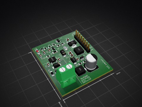
It measures 168 × 61 mm and has 2 copper layers, 1.6 mm thick.
72 parts, built around the ATMEGA328P-PU, ESP-WROOM-02, TXS0101DBV and MMBTA06. The full list of its parts is on this page, with links to each part's symbol and footprint where PCBKit's library has them.
From the dhanush-darpan/Smart-Home-Automation-Controller-PCB repository on GitHub, at the commit this page was made from: the board is smart_home_automation_controller.kicad_pcb and its schematic smart_home_automation_controller.kicad_sch. PCBKit opens the board in the browser, with nothing to install.
Its repository states no licence, so its author keeps all rights: ask dhanush-darpan before reusing the design.