

2 layers61 × 61 mm
ESP32 FC
MAATHES-THILAK-K/ESP32-S3_FLIGHT_CONTROLLER
A custom-designed flight controller based on the ESP32-S3 module, built for compatibility with the esp-fc firmware and Betaflight-like configuration.
69 parts7Apache-2.0

An integrated PCB power management system for single-cell Li-Po batteries featuring onboard charging, circuit protection, and a DC-DC boost converter with selectable 5V and 12V DC outputs. Includes full open-source KiCad schematics, PCB layout files, complete BOM, and manufacturing Gerber files.
Project2 is an open-source printed circuit board by devKOff, from the devKOff/pcb-lipo-power-management-system repository on GitHub. It is a 2-layer board of 30 × 25 mm with 28 parts on 28 nets, routed with 226 tracks and 23 vias.
It is built around the MT3608, TP4056-42-ESOP8 and DW01A, with the FS8205A and SS34 among its other parts. Its parts include 10 resistors, 5 connectors, 4 capacitors, 3 diodes and 2 ICs. It belongs with the power boards of this library.


A compact, integrated PCB for Li-Po battery charging, protection, and switch-selectable 5 V / 12 V output.
Combines a TP4056 Li-Po charging stage, DW01A/FS8205A battery protection, and an MT3608 boost converter on a single two-layer board — designed for portable electronics, IoT nodes, Arduino-based projects, and lightweight UAV subsystems.




| Board name | Project 2 — Power Management System |
| Function | Li-Po charging + protection + selectable 5 V/12 V boost output |
| Charging IC | TP4056 (USB Type-C input, CC/CV charging) |
| Protection ICs | DW01A + FS8205A (overcharge / over-discharge / overcurrent) |
| Boost converter | MT3608 (switch-selectable ≈5 V / ≈12 V output) |
| Layers | 2-layer PCB |
| EDA tool | KiCad v10 |
| Isometric View | Top View | Bottom View |
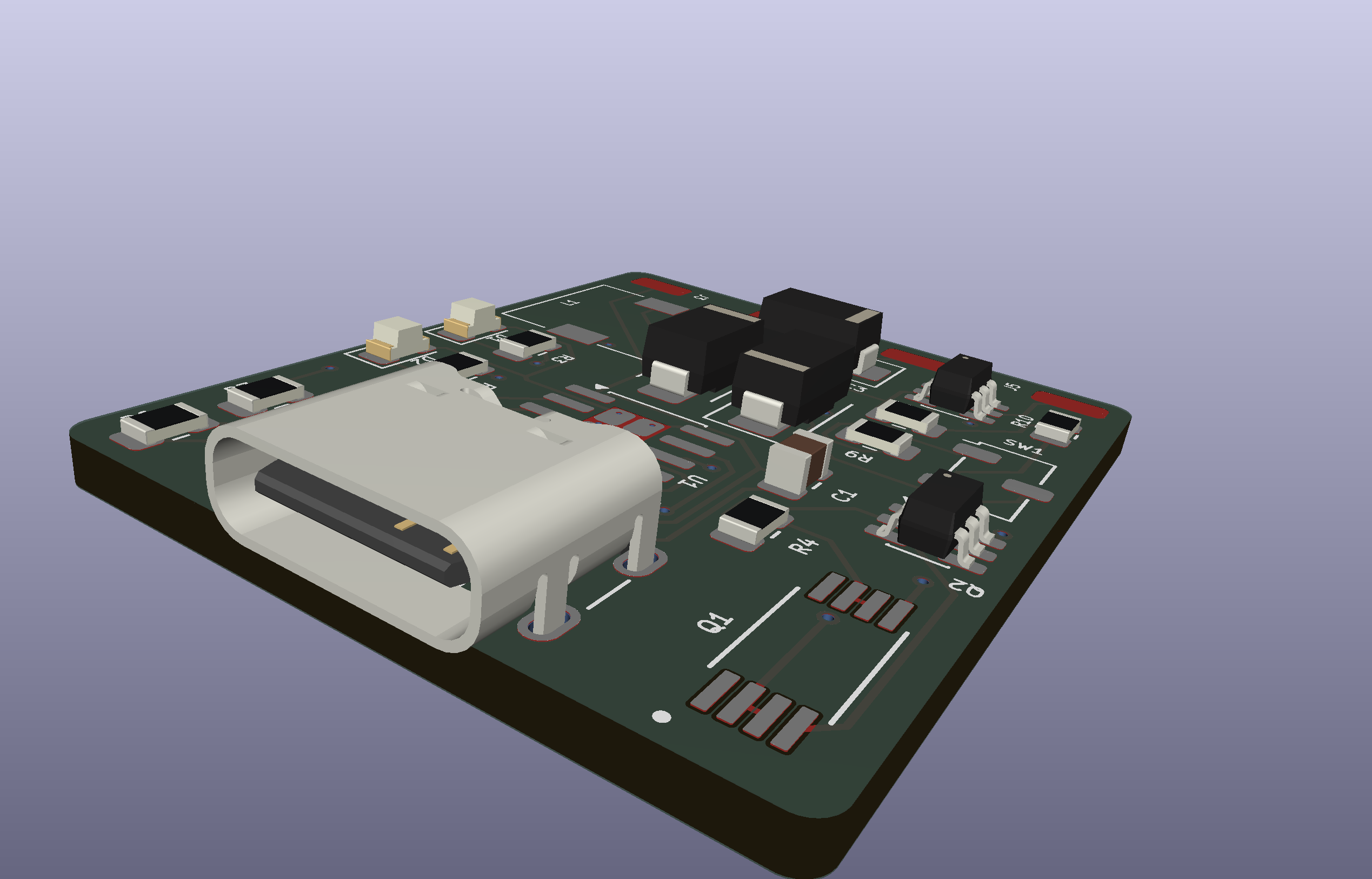 | 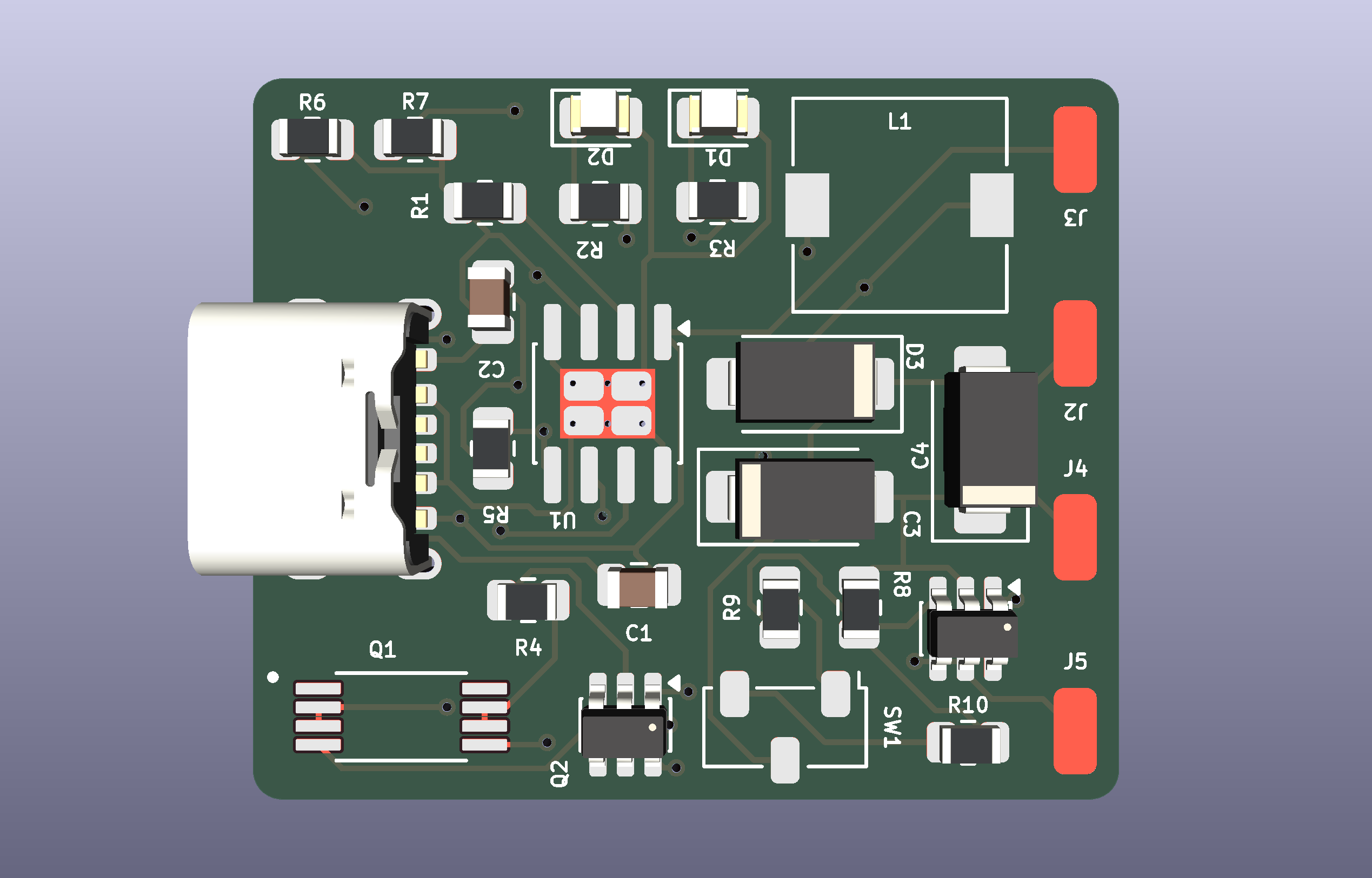 | 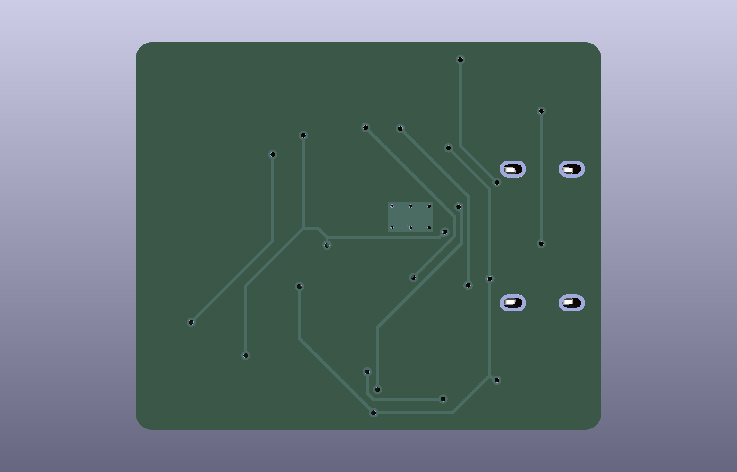 |
Full schematic of the charging, protection, and boost-conversion circuitry:
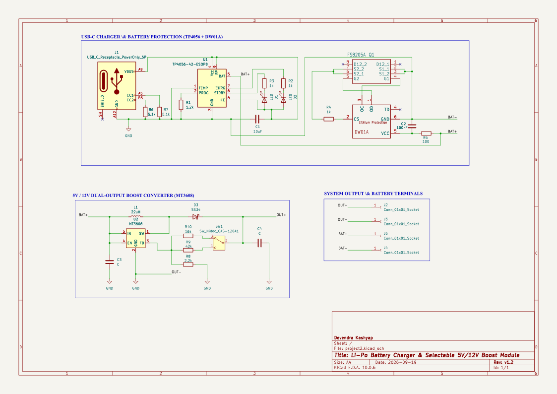
If the vector render above does not display (GitHub occasionally sandboxes inline SVG), open it directly:
docs/images/schematics/project2.svg. A PNG fallback may also be available atdocs/images/schematics/project2.png.
| Top Copper (F.Cu) | Bottom Copper (B.Cu) |
|---|---|
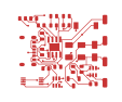 | 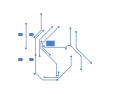 |
| Top Silkscreen (F.Silkscreen) | Bottom Silkscreen (B.Silkscreen) |
|---|---|
 |  |
| Board Outline (Edge.Cuts) |
|---|
 |
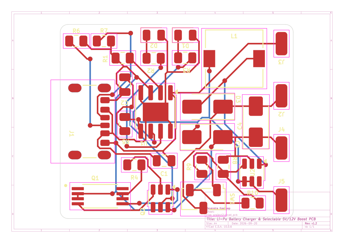
| Top Solder Mask (F.Mask) | Bottom Solder Mask (B.Mask) |
|---|---|
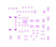 |  |
| Deliverable | Description | Link |
|---|---|---|
| 📋 Bill of Materials | Full component list with references, values, and quantities | docs/power_management_system_bom.csv |
| 🏭 Gerber Files | Fabrication-ready Gerber package for PCB manufacturing | gerbers/ |
| 🧩 STEP 3D CAD File | Mechanical 3D model for enclosure/assembly integration | step/ |
| 🗂️ KiCad Project | Top-level KiCad project file | project2.kicad_pro |
| 🔲 KiCad PCB Layout | Editable PCB layout file | project2.kicad_pcb |
| ⚡ KiCad Schematic | Editable schematic source file | project2.kicad_sch |
Note: If the BOM is provided as a spreadsheet instead of CSV, use
docs/power_management_system_bom.xlsx.
pcb-lipo-power-management-system/
├── docs/
│   ├── images/
│   │   ├── 3d_views/
│   │   │   ├── 3d_top.png
│   │   │   ├── 3d_iso.png
│   │   │   └── 3d_bottom.png
│   │   ├── schematics/
│   │   │   └── project2.svg
│   │   └── pcb_layers/
│   │       ├── pcb_All_layers.svg
│   │       ├── project2-F_Cu.svg
│   │       ├── project2-B_Cu.svg
│   │       ├── project2-F_Silkscreen.svg
│   │       ├── project2-B_Silkscreen.svg
│   │       ├── project2-F_Mask.svg
│   │       ├── project2-B_Mask.svg
│   │       └── project2-Edge_Cuts.svg
│   └── power_management_system_bom.csv
├── gerbers/
│   └── (fabrication Gerber + drill files)
├── step/
│   └── (STEP 3D CAD export)
├── assets/Note:
.history/,DRC.rpt,report.txt, andtemp-freerouting.dsnare local KiCad/tooling artifacts. Consider adding them to.gitignoreif they don't need to be version-controlled — they're listed here only for completeness.
git clone https://github.com/devKOff/pcb-lipo-power-management-system.git
cd pcb-lipo-power-management-systemproject2.kicad_pro in KiCad to view or edit the schematic and PCB layout.gerbers/ directly to your PCB fabricator, and reference
docs/power_management_system_bom.csv for assembly.step/ into your CAD tool of choice for enclosure or
assembly design.This project is released under the terms of the MIT License. Hardware design files are shared in the spirit of open source hardware — see the OSHW badge above.
Note: No
LICENSEfile currently exists in this repository. Add one (e.g. via GitHub's Add file → Create new file → LICENSE flow, which offers an MIT template) so the badge and link above resolve correctly — see Step 6 in the upload guide below.
Maintained as part of the Project 2 — Power Management System hardware design effort.
| Qty | Value | Footprint | References |
|---|---|---|---|
| 4 | Conn_01x01_Socket | Connector_Wire:SolderWirePad_1x01_SMD_1.5x3mm | J2, J3, J4, J5 |
| 3 | 1k | Resistor_SMD:R_0805_2012Metric | R2, R3, R4 |
| 2 | 5.1k | Resistor_SMD:R_0805_2012Metric | R6, R7 |
| 2 | C | Diode_SMD:D_SMA | C3, C4 |
| 2 | LED | LED_SMD:LED_0805_2012Metric | D1, D2 |
| 1 | 1.2k | Resistor_SMD:R_0805_2012Metric | R1 |
| 1 | 100 | Resistor_SMD:R_0805_2012Metric | R5 |
| 1 | 100nF | Capacitor_SMD:C_0805_2012Metric | C2 |
| 1 | 10uF | Capacitor_SMD:C_0805_2012Metric | C1 |
| 1 | 16k | Resistor_SMD:R_0805_2012Metric | R10 |
| 1 | 2.2k | Resistor_SMD:R_0805_2012Metric | R8 |
| 1 | 22uH | Inductor_SMD:L_7.3x7.3_H4.5 | L1 |
| 1 | 42k | Resistor_SMD:R_0805_2012Metric | R9 |
| 1 | DW01A | Package_TO_SOT_SMD:SOT-23-6 | Q2 |
| 1 | FS8205A | FS8205A:SOP65P640X120-8N | Q1 |
| 1 | MT3608 | Package_TO_SOT_SMD:SOT-23-6 | U2 |
| 1 | SS34 | Diode_SMD:D_SMA | D3 |
| 1 | SW_Nidec_CAS-120A1 | Button_Switch_SMD:Nidec_Copal_CAS-120A | SW1 |
| 1 | TP4056-42-ESOP8 | Package_SO:SOIC-8-1EP_3.9x4.9mm_P1.27mm_EP2.41x3.3mm_ThermalVias | U1 |
| 1 | USB_C_Receptacle_PowerOnly_6P | Connector_USB:USB_C_Receptacle_GCT_USB4125-xx-x_6P_TopMnt_Horizontal | J1 |
MAATHES-THILAK-K/ESP32-S3_FLIGHT_CONTROLLER
A custom-designed flight controller based on the ESP32-S3 module, built for compatibility with the esp-fc firmware and Betaflight-like configuration.

nikolaus018/dji-fcc-esp32
ESP32-S3 firmware that switches a DJI N1 remote to FCC mode over USB (replaces the Android app)


luke-walsh1/FLIGHT
A custom, high-performance rocket flight computer designed around a Raspberry Pi Pico (RP2040) to track, log, and deploy parachutes using a servo motor.


wngxp/aqi-monitor
A custom indoor air-quality monitor with particulate, carbon-dioxide, temperature, humidity, and pressure sensing; a round color display; a nine-pixel status gauge; and an optional connected backend and mobile app.

houseofthe051010/ESP32-Walkie-Talkie-V2
This ESP32 Walkie Talkie is redesigned with a SX1262 radio, a PCB, and a full case redesign.
It measures 30 × 25 mm and has 2 copper layers, 1.6 mm thick.
28 parts, built around the MT3608, TP4056-42-ESOP8, DW01A and FS8205A. The full list of its parts is on this page, with links to each part's symbol and footprint where PCBKit's library has them.
From the devKOff/pcb-lipo-power-management-system repository on GitHub, at the commit this page was made from: the board is project2.kicad_pcb and its schematic project2.kicad_sch. PCBKit opens the board in the browser, with nothing to install.
Its repository states no licence, so its author keeps all rights: ask devKOff before reusing the design.