
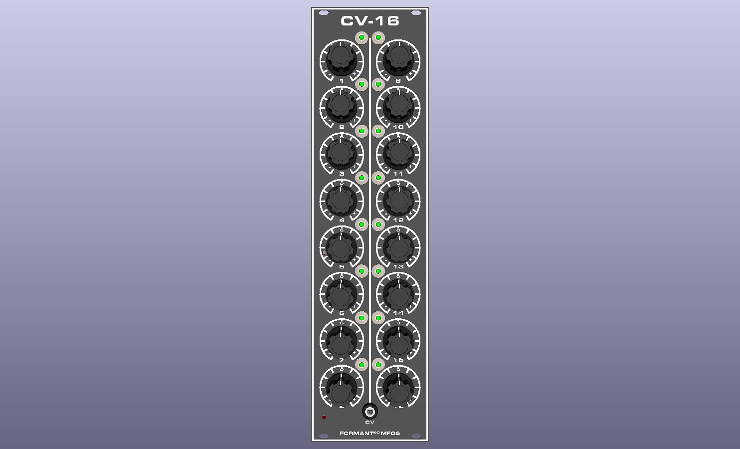
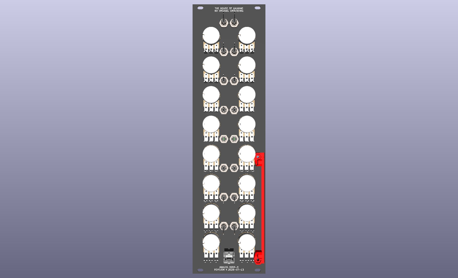
2 layers160 × 100 mm
CLOCK
Desval27/FormantKO
Knock-off of the Elektor Formant Synthesizer project with the initial goal of being quasi-authentic and secondary goal undecided. Probably tweaks of some kind.
135 partsMIT

 Desval27/FormantKO
Knock-off of the Elektor Formant Synthesizer project with the initial goal of being quasi-authentic and secondary goal undecided. Probably tweaks of some kind.
TEST HARNESS is an open-source printed circuit board by Desval27, from the Desval27/FormantKO repository on GitHub, published under the MIT licence. It is a 2-layer board of 127 × 104.1 mm with 38 parts on 69 nets, routed with 316 tracks and 0 vias.
It is built around the CT3151SP-0. Its parts include 9 resistors, 7 diodes, 6 capacitors, 6 connectors and 4 switches. It belongs with the audio and music boards of this library.
| Qty | Value | Footprint | References |
|---|---|---|---|
| 4 | 10k | FormantKO:R_Axial_Horizontal | R1, R4, R8, R10 |
| 4 | CT3151SP-0 | FormantKO:Banana_Jack_Horizontal | J2, J3, J4, J5 |
| 3 | 100n | Capacitor_THT:C_Disc_D10.0mm_W2.5mm_P5.00mm | C1, C2, C3 |
| 3 | 150R | FormantKO:R_Axial_Horizontal | R6, R9, R11 |
| 3 | 47µ | Capacitor_THT:CP_Radial_D6.3mm_P2.50mm | C4, C5, C6 |
| 2 | 10k | FormantKO:Potentiometer_Alps_RK09K_Single_Vertical | RV1, RV2 |
| 2 | 2N3904 | Package_TO_SOT_THT:TO-92L_Wide | Q1, Q2 |
| 2 | 680R | FormantKO:R_Axial_Horizontal | R5, R7 |
| 2 | DUS | FormantKO:DUS | D6, D7 |
| 2 | MountingHole | FormantKO:MountingHole_2.7mm_M2.5 | H2, H4 |
| 1 | +15V | LED_THT:LED_D5.0mm | D1 |
| 1 | +5V | LED_THT:LED_D5.0mm | D2 |
| 1 | -15V | LED_THT:LED_D5.0mm | D3 |
| 1 | Conn_02x16_Odd_Even | Connector_PinHeader_2.54mm:PinHeader_2x16_P2.54mm_Vertical | J6 |
| 1 | GATE1 | Button_Switch_THT:SW_PUSH_6mm_H4.3mm | SW1 |
| 1 | GATE1 | LED_THT:LED_D5.0mm | D4 |
| 1 | GATE2 | Button_Switch_THT:SW_PUSH_6mm_H4.3mm | SW2 |
| 1 | GATE2 | LED_THT:LED_D5.0mm | D5 |
| 1 | KOV1 | FormantKO:Switch_Toggle_SPDT_SubMini_PCB | SW3 |
| 1 | KOV2 | FormantKO:Switch_Toggle_SPDT_SubMini_PCB | SW4 |
| 1 | SLOT 1 | FormantKO:BusConnectorTest | J1 |
Desval27/FormantKO
Knock-off of the Elektor Formant Synthesizer project with the initial goal of being quasi-authentic and secondary goal undecided. Probably tweaks of some kind.

Desval27/FormantKO
Knock-off of the Elektor Formant Synthesizer project with the initial goal of being quasi-authentic and secondary goal undecided. Probably tweaks of some kind.

Desval27/FormantKO
Knock-off of the Elektor Formant Synthesizer project with the initial goal of being quasi-authentic and secondary goal undecided. Probably tweaks of some kind.

Desval27/FormantKO
Knock-off of the Elektor Formant Synthesizer project with the initial goal of being quasi-authentic and secondary goal undecided. Probably tweaks of some kind.

Desval27/FormantKO
Knock-off of the Elektor Formant Synthesizer project with the initial goal of being quasi-authentic and secondary goal undecided. Probably tweaks of some kind.

Desval27/FormantKO
Knock-off of the Elektor Formant Synthesizer project with the initial goal of being quasi-authentic and secondary goal undecided. Probably tweaks of some kind.

Desval27/FormantKO
Knock-off of the Elektor Formant Synthesizer project with the initial goal of being quasi-authentic and secondary goal undecided. Probably tweaks of some kind.

Desval27/FormantKO
Knock-off of the Elektor Formant Synthesizer project with the initial goal of being quasi-authentic and secondary goal undecided. Probably tweaks of some kind.

Desval27/FormantKO
Knock-off of the Elektor Formant Synthesizer project with the initial goal of being quasi-authentic and secondary goal undecided. Probably tweaks of some kind.

Desval27/FormantKO
Knock-off of the Elektor Formant Synthesizer project with the initial goal of being quasi-authentic and secondary goal undecided. Probably tweaks of some kind.

Desval27/FormantKO
Knock-off of the Elektor Formant Synthesizer project with the initial goal of being quasi-authentic and secondary goal undecided. Probably tweaks of some kind.

Desval27/FormantKO
Knock-off of the Elektor Formant Synthesizer project with the initial goal of being quasi-authentic and secondary goal undecided. Probably tweaks of some kind.


ssyhy9-Hongyu/MS_Thesis_PCB
PCB version control for current source inverter project

joeycastillo/The-Open-Book
For details on how to build, test and use Open Book, I've made documentation available here.


hackclub/OnBoard
💡 Join 1,000 teenagers and make your first PCB with a $100 grant!
It measures 127 × 104.1 mm and has 2 copper layers, 1.6 mm thick.
38 parts, built around the CT3151SP-0. The full list of its parts is on this page, with links to each part's symbol and footprint where PCBKit's library has them.
From the Desval27/FormantKO repository on GitHub, at the commit this page was made from: the board is system/TEST_HARNESS/TEST_HARNESS.kicad_pcb. PCBKit opens the board in the browser, with nothing to install.
Its repository publishes it under the MIT licence: you may reuse it on that licence's terms (keep the author's notice, and for a copyleft licence share your changes alike).