2 layers77.5 × 120.5 mm
Gameboy v1
yashlohar20/gameboy-v1
DIY handheld game console — custom PCB, STM32 firmware, full hardware stack
39 parts

 DerRKDCB/meshphone5
meshtastic Samsung Galaxy A5 standalone offline dual node
Galaxy A5 dual node is an open-source printed circuit board by DerRKDCB, from the DerRKDCB/meshphone repository on GitHub. It is a 2-layer board of 60 × 80 mm with 87 parts on 113 nets, routed with 564 tracks and 80 vias.
It is built around the RAK4630, TPS62203DBV and CH334R, with the DW01, FS8205A and TP4056-42-ESOP8 among its other parts. Its parts include 22 resistors, 18 capacitors, 7 ICs, 7 diodes and 5 connectors. It belongs with the radio and wireless boards of this library.


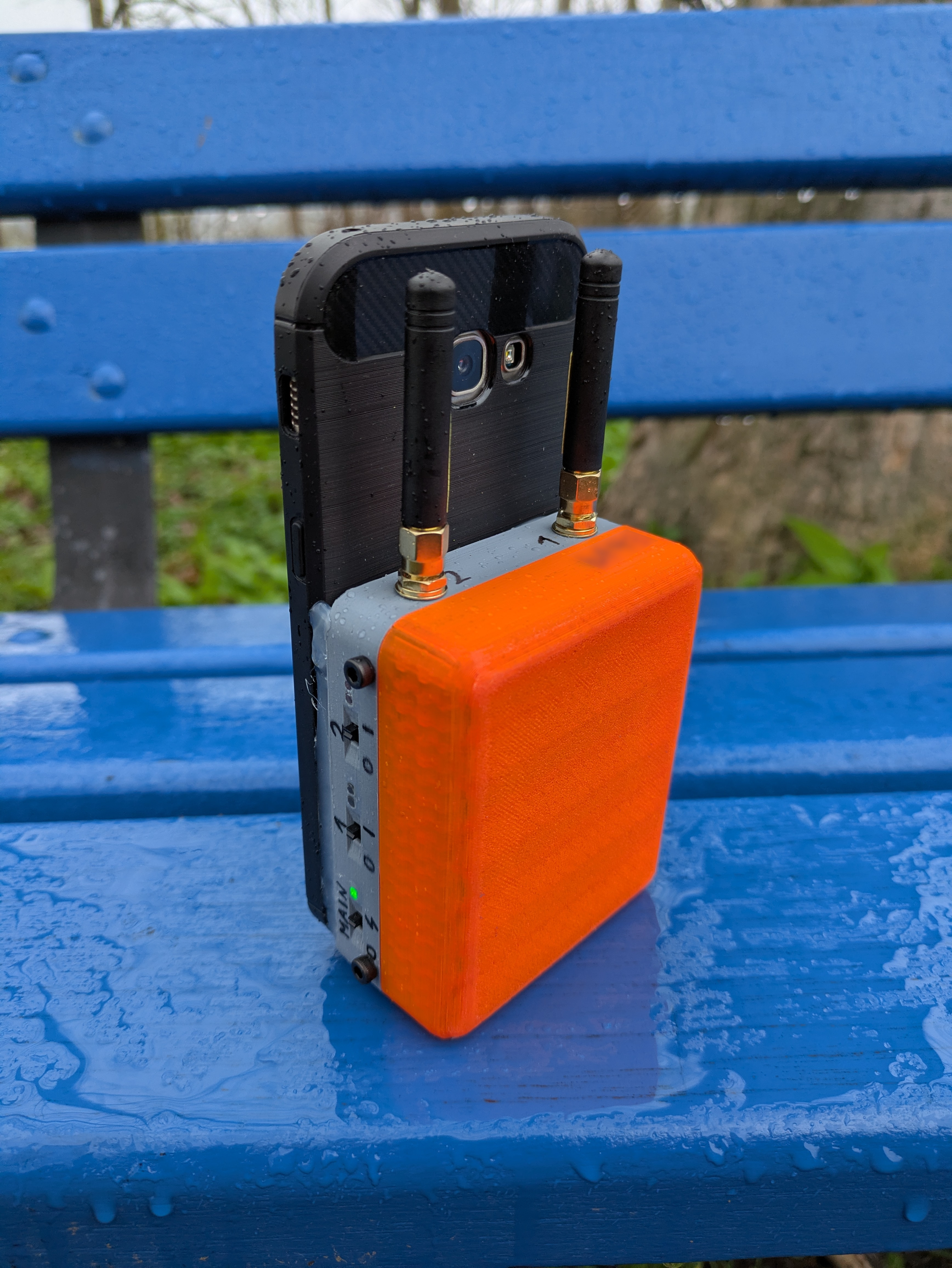
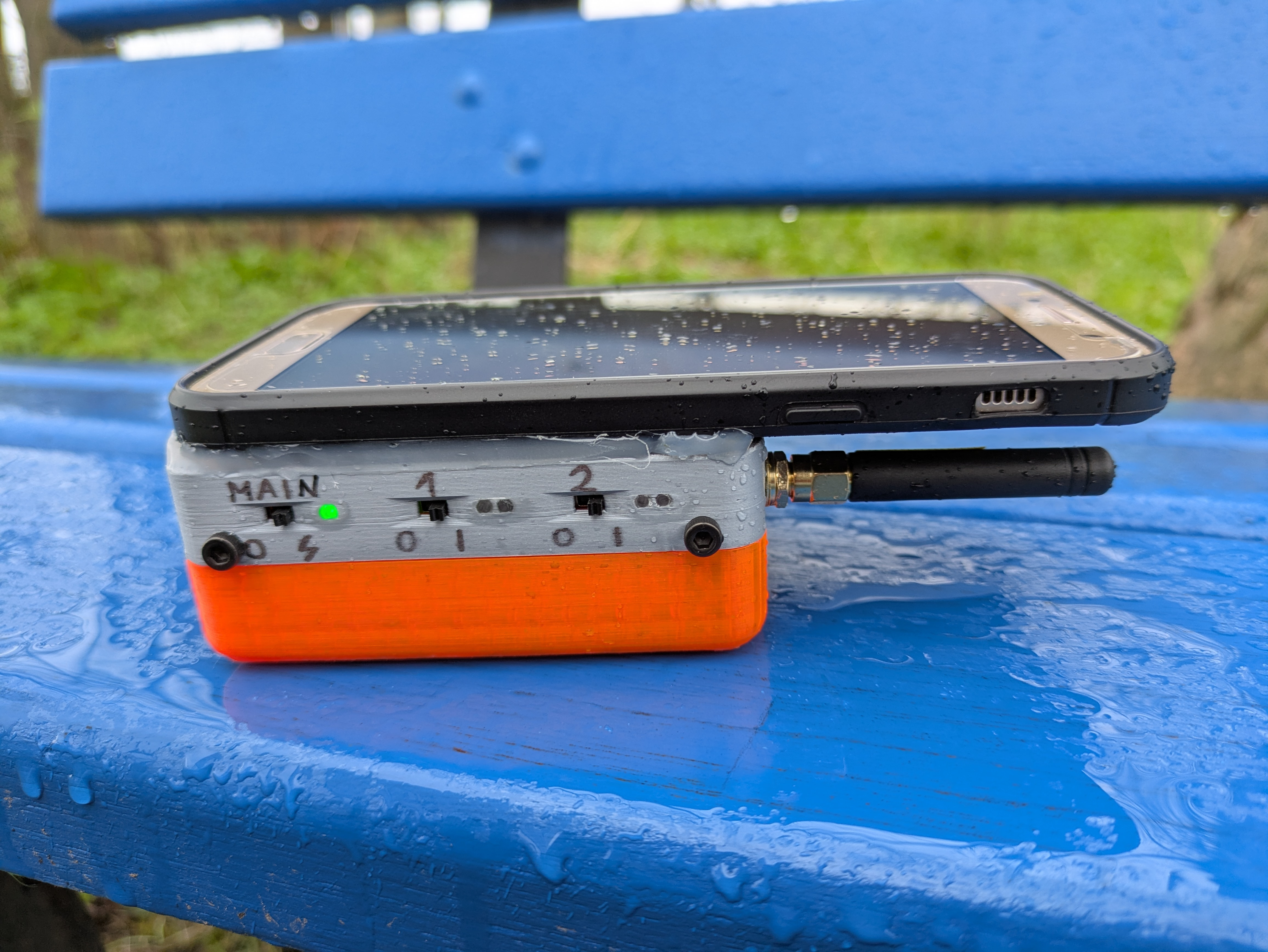
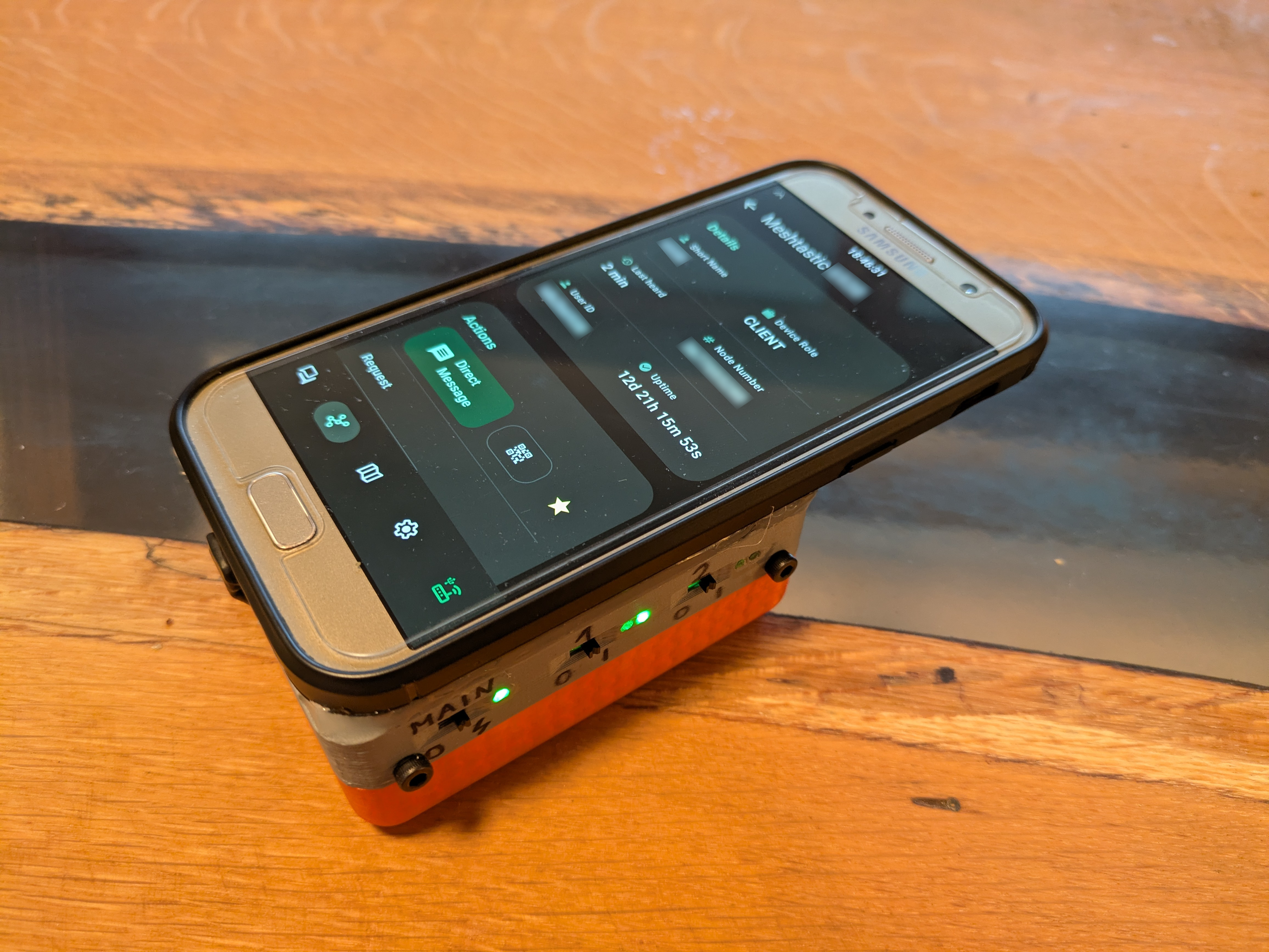
A standalone dual-node Meshtastic/MeshCore device built into a Samsung Galaxy A5 form factor.
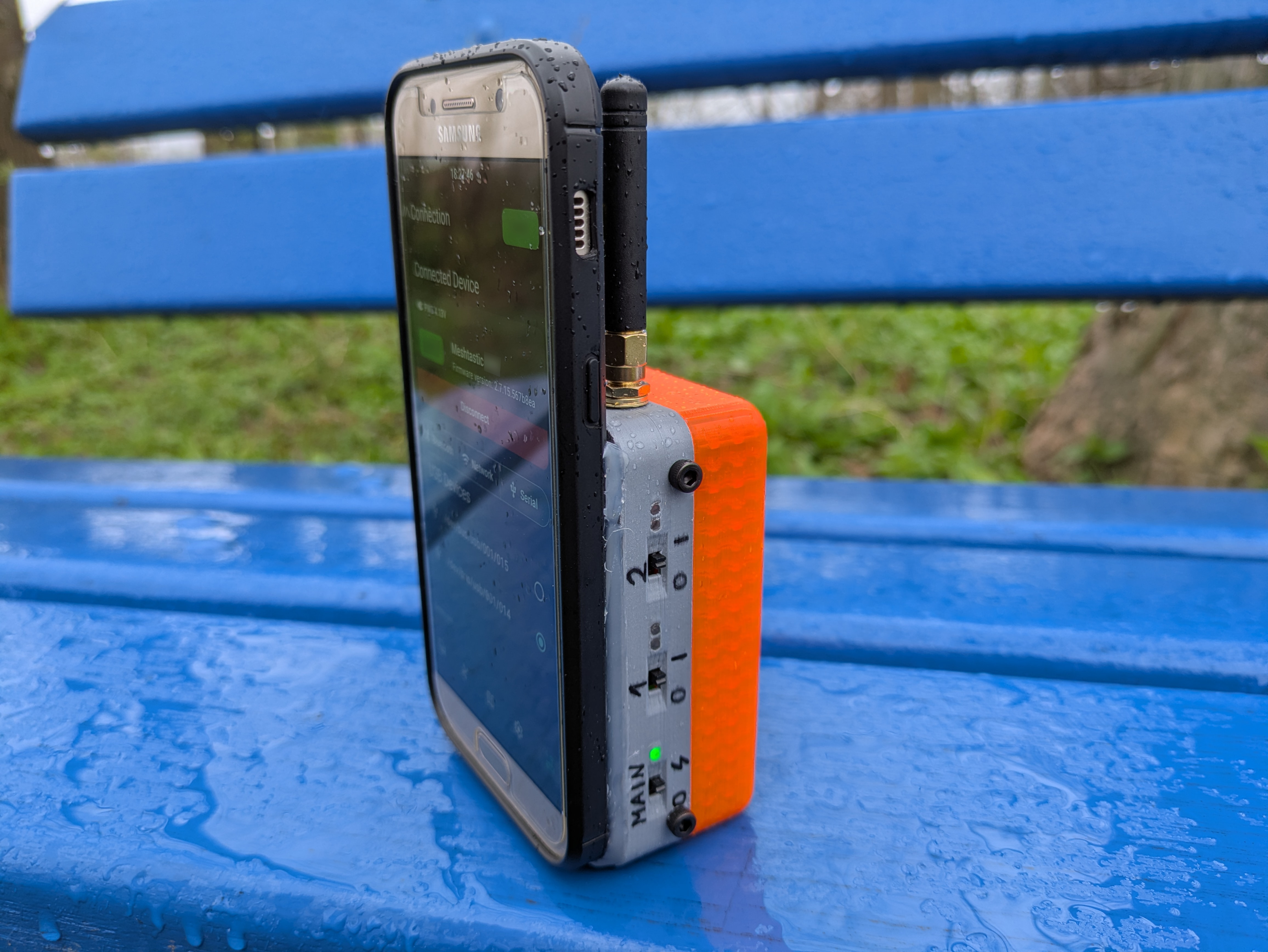
Meshphone is a custom dual-node Meshtastic device featuring:
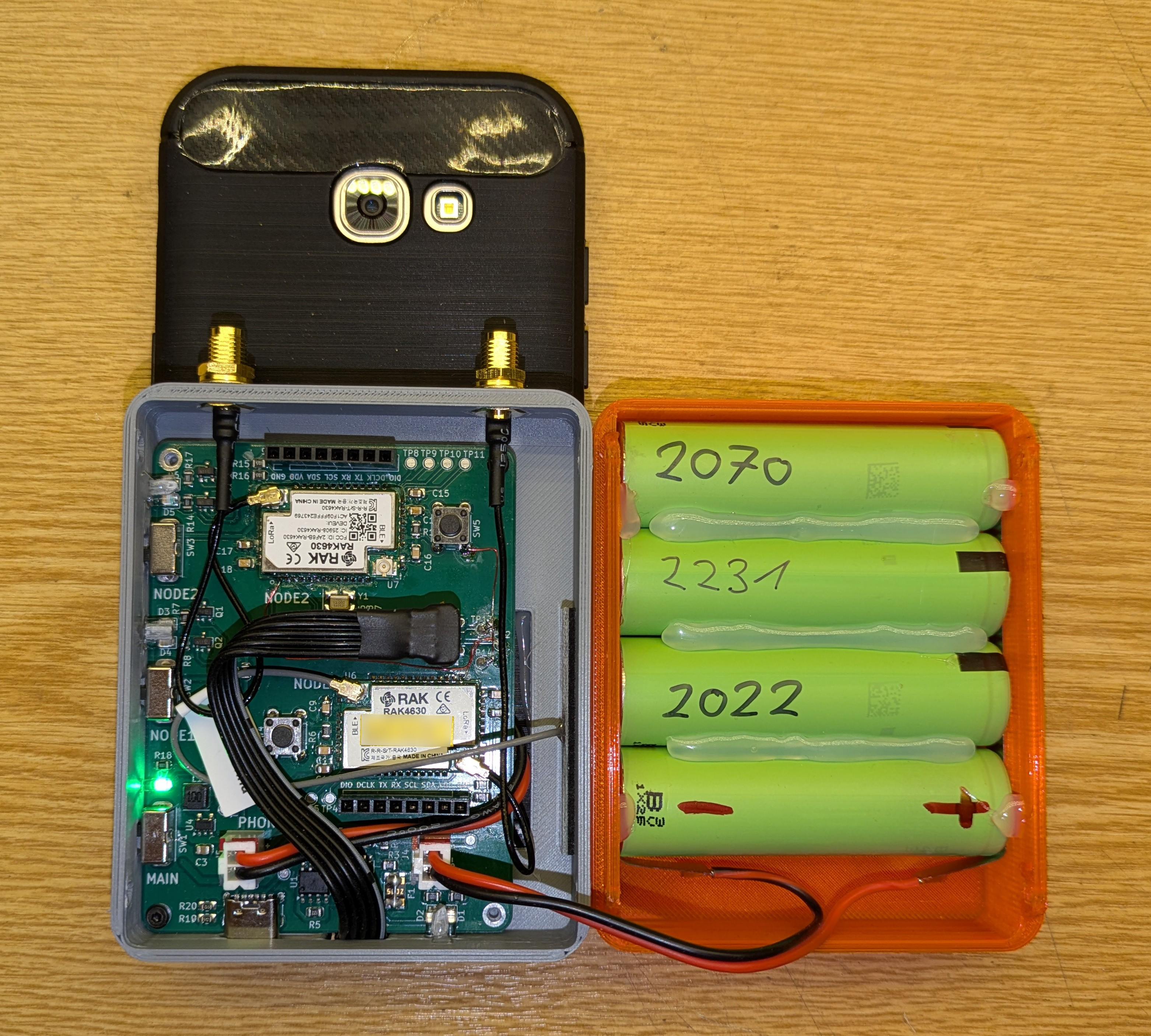
Off-the-shelf standalone devices like the T-Deck lack the full feature set available in Meshtastic/MeshCore. By making it a dual-node device, I can run two different configurations simultaneously. The nodes connect through a USB hub IC - a cleaner solution than Bluetooth coupling with potential radio interference over short distances.
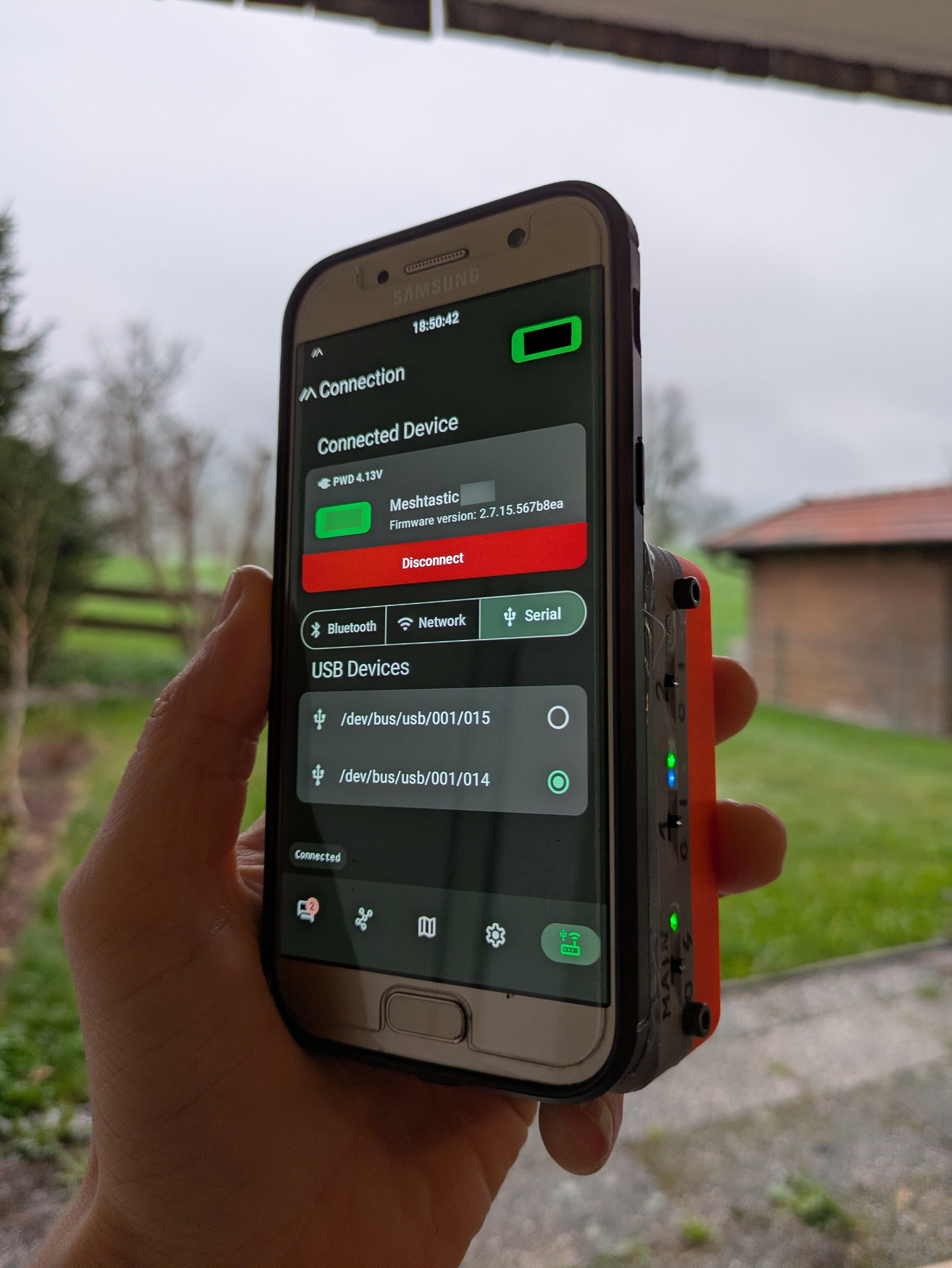
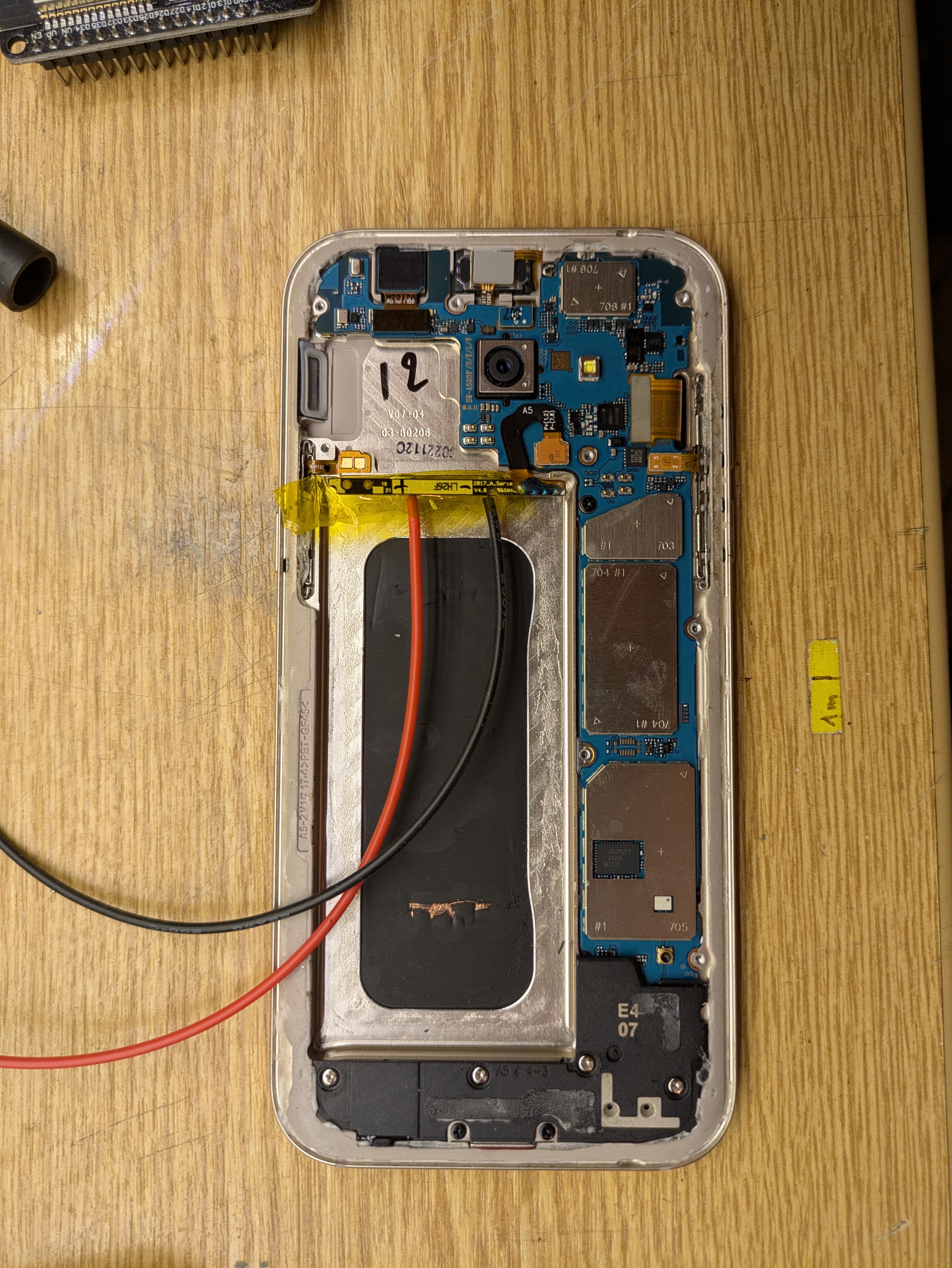
The Galaxy A5's internal battery was removed and replaced with external power from the PCB via cables. This allows complete disconnection via switch and increased battery capacity. The phone sits in a cheap TPU case, with 3D printed PLA housing for the nodes and batteries, secured with hot glue.
RAK4630 Modules - Chosen for:
Reference designs: RAK4631 and RAK19003 modules.
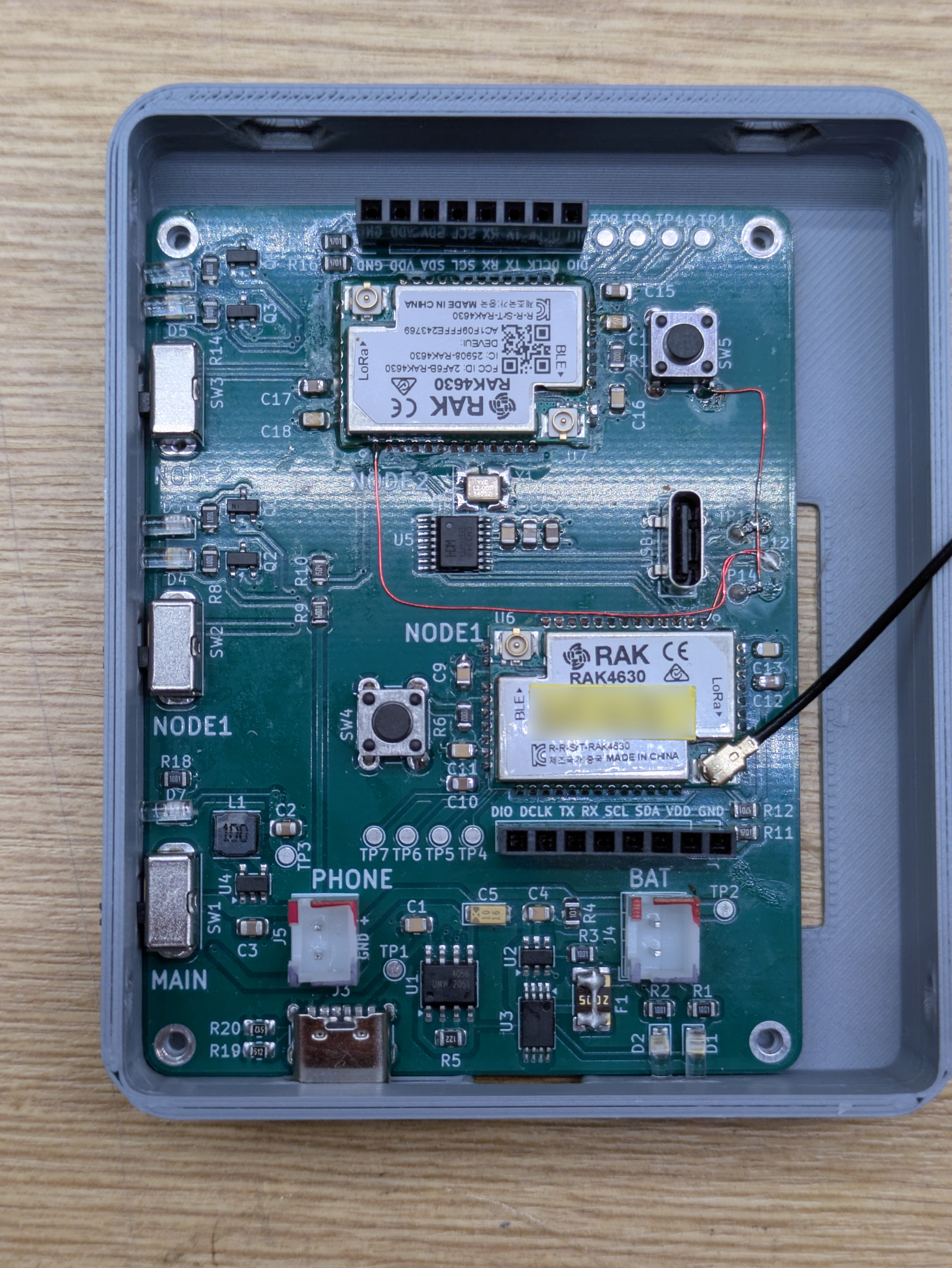
Note: The RAK USB port requires 5V on VBUS to initialize - learned this during integration and had to bodge it. Fixed in the PCB design.
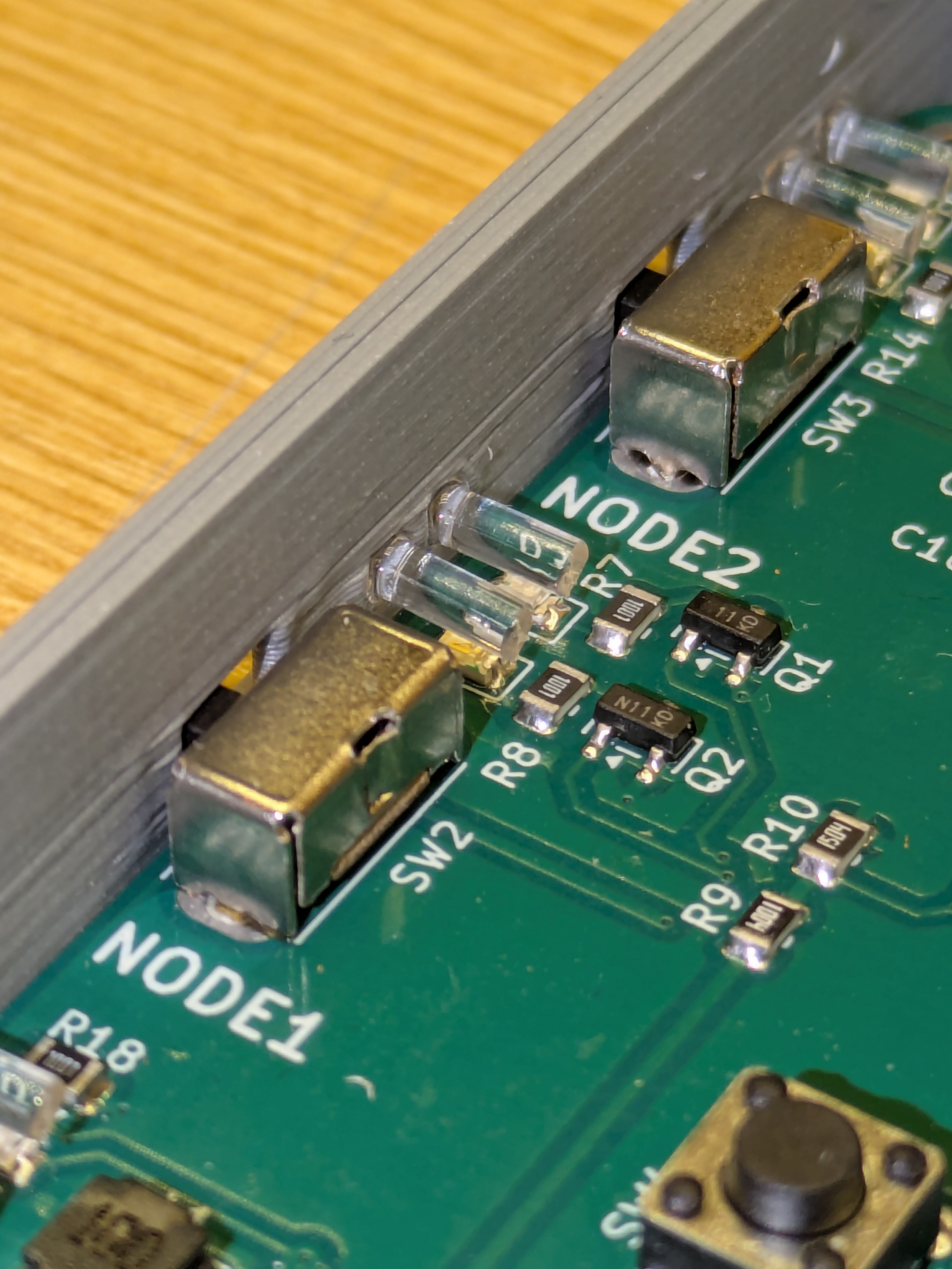
Status LEDs (7 total):
Light channels made from clear PETG filament - works awesome!
Battery Management:
USB Hub - CH334P:
3.3V Supply: TI TPS62203DBVT low-power buck converter
Bodged during build:
Remaining issue: When switching on either node, the hub disconnects and reconnects completely, making it impossible to differentiate which node is which USB device. Not sure why this happens, but it's manageable.
This project was an awesome learning experience and I love the result. For future versions I'd do some things differently - most likely keeping the battery in the phone and supplying the whole PCB from the phone's USB port.
by DerRKDCB
| Qty | Value | Footprint | References |
|---|---|---|---|
| 9 | 100nF | Capacitor_SMD:C_0805_2012Metric | C1, C4, C6, C9, C11, C13, C14, C16, C18 |
| 8 | 1k | Resistor_SMD:R_0805_2012Metric | R1, R2, R3, R7, R8, R14, R17, R18 |
| 6 | 10uF | Capacitor_SMD:C_0805_2012Metric | C2, C7, C10, C12, C15, C17 |
| 4 | 4.7k | Resistor_SMD:R_0805_2012Metric | R11, R12, R15, R16 |
| 4 | 5.1k | Resistor_SMD:R_0805_2012Metric | R19, R20, R21, R22 |
| 4 | DTC143Z | Package_TO_SOT_SMD:SOT-23 | Q1, Q2, Q3, Q4 |
| 4 | MountingHole_Pad | MountingHole:MountingHole_2.2mm_M2_DIN965_Pad_TopBottom | H1, H2, H3, H4 |
| 3 | LEDB | LED_SMD:LED_0805_2012Metric | D2, D4, D5 |
| 3 | LEDG | LED_SMD:LED_0805_2012Metric | D3, D6, D7 |
| 2 | 10k | Resistor_SMD:R_0805_2012Metric | R6, R13 |
| 2 | Conn | Connector_PinHeader_2.54mm:PinHeader_1x08_P2.54mm_Vertical | J1, J2 |
| 2 | Conn_01x02_Socket | Connector_JST:JST_XH_B2B-XH-A_1x02_P2.50mm_Vertical | J4, J5 |
| 2 | DE0 | TestPoint:TestPoint_Pad_D1.5mm | TP7, TP11 |
| 2 | DE1 | TestPoint:TestPoint_Pad_D1.5mm | TP4, TP8 |
| 2 | RAK4630 | galaxy_a5_node:rak4630 | U6, U7 |
| 2 | RX0 | TestPoint:TestPoint_Pad_D1.5mm | TP5, TP9 |
| 2 | SW_RST | Button_Switch_THT:SW_PUSH_6mm_H5mm | SW4, SW5 |
| 2 | TX0 | TestPoint:TestPoint_Pad_D1.5mm | TP6, TP10 |
| 1 | 1.2k | Resistor_SMD:R_0805_2012Metric | R5 |
| 1 | 1.5M | Resistor_SMD:R_0805_2012Metric | R10 |
| 1 | 100 | Resistor_SMD:R_0805_2012Metric | R4 |
| 1 | 10uF | Capacitor_Tantalum_SMD:CP_EIA-3216-12_Kemet-S | C5 |
| 1 | 10uH | Inductor_SMD:L_APV_ANR4018 | L1 |
| 1 | 1M | Resistor_SMD:R_0805_2012Metric | R9 |
| 1 | 1uF | Capacitor_SMD:C_0805_2012Metric | C8 |
| 1 | 4.7uF | Capacitor_SMD:C_0805_2012Metric | C3 |
| 1 | 500mA | Fuse:Fuse_1812_4532Metric_Pad1.30x3.40mm_HandSolder | F1 |
| 1 | CH334R | Package_SO:QSOP-16_3.9x4.9mm_P0.635mm | U5 |
| 1 | Crystal 12MHz | Crystal:Crystal_SMD_3225-4Pin_3.2x2.5mm_HandSoldering | Y1 |
| 1 | DW01 | Package_TO_SOT_SMD:SOT-23-6 | U2 |
| 1 | FS8205A | Package_SO:TSSOP-8_4.4x3mm_P0.65mm | U3 |
| 1 | GT-USB-7055BB | lcsc:USB-C-TH_GT-USB-7055BB | USB1 |
| 1 | LEDR | LED_SMD:LED_0805_2012Metric | D1 |
| 1 | SW_MAIN | Button_Switch_THT:SW_Slide_SPDT_Angled_CK_OS102011MA1Q | SW1 |
| 1 | SW_RAK1 | Button_Switch_THT:SW_Slide_SPDT_Angled_CK_OS102011MA1Q | SW2 |
| 1 | SW_RAK2 | Button_Switch_THT:SW_Slide_SPDT_Angled_CK_OS102011MA1Q | SW3 |
| 1 | TP4056-42-ESOP8 | Package_SO:SOIC-8-1EP_3.9x4.9mm_P1.27mm_EP2.41x3.3mm_ThermalVias | U1 |
| 1 | TPS62203DBV | Package_TO_SOT_SMD:SOT-23-5 | U4 |
| 1 | USB_C_Receptacle_PowerOnly_6P | Connector_USB:USB_C_Receptacle_GCT_USB4125-xx-x_6P_TopMnt_Horizontal | J3 |
| 1 | VBAT | TestPoint:TestPoint_Pad_D1.5mm | TP2 |
| 1 | VCHRG | TestPoint:TestPoint_Pad_D1.5mm | TP1 |
| 1 | VDD | TestPoint:TestPoint_Pad_D1.5mm | TP3 |
It measures 60 × 80 mm and has 2 copper layers, 1.6 mm thick.
87 parts, built around the RAK4630, TPS62203DBV, CH334R and DW01. The full list of its parts is on this page, with links to each part's symbol and footprint where PCBKit's library has them.
From the DerRKDCB/meshphone repository on GitHub, at the commit this page was made from: the board is kicad/galaxy_A5_dual_node/galaxy_A5_dual_node.kicad_pcb and its schematic kicad/galaxy_A5_dual_node/galaxy_A5_dual_node.kicad_sch. PCBKit opens the board in the browser, with nothing to install.
Its repository states no licence, so its author keeps all rights: ask DerRKDCB before reusing the design.
yashlohar20/gameboy-v1
DIY handheld game console — custom PCB, STM32 firmware, full hardware stack

AndreiVladescu/LibrePLC32
The goal of the project is to create a compact, hackable, and well-documented PLC platform for industrial automation experiments, prototyping, education, and open hardware development.

ciaassured/eveningstar-hardware
Hardware design for the Eveningstar ESP32-based Morningstar MeterBus interface.

ISS-Lab-Unibo/Agro_LoRaInductiveFruitGauge
An open-source, low-cost and low-power LoRaWAN sensor node for continuous, non-destructive monitoring of fruit growth directly on the tree, together with the high-resolution inductive fruit gauges (pliers) it reads.


mornepousse/Niphargus
Niphargus — a slim, indestructible wireless split keyboard. ESP32 + nRF24, wired fallback, and an emergency kit hidden behind the USB port. The successor to the Rouge-Gorge.


fishPointer/Joule-Thief
I teach myself new skills by designing projects that require to develop the skills I want in order to complete them.