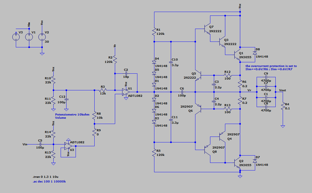
Design and simulation of a Class-AB audio power amplifier, focusing on output-stage linearity, crossover distortion reduction, and overcurrent protection.
Mono amplifier is an open-source printed circuit board by dario0603, from the dario0603/AB-class-amplifier repository on GitHub. It is a 2-layer board of 120.1 × 120 mm with 97 parts on 53 nets, routed with 482 tracks and 69 vias.
It is built around the TL081, BC327 and BC337, with the TIP3055, BD139 and BD140 among its other parts. Its parts include 41 capacitors, 26 resistors, 9 diodes, 9 connectors and 8 transistors. It belongs with the audio and music boards of this library.
Design and simulation of a Class-AB audio power amplifier, focusing on output-stage linearity, crossover distortion reduction, and overcurrent protection.
The circuit combines an input amplification stage, diode-based biasing, and a complementary power output stage to achieve linear signal amplification. LTspice simulations are used to investigate the amplifier's transient response, frequency behavior, and current-limiting operation.
The project also explores the interaction between output-stage biasing, load current, and protection circuitry.
Design Calculations
1. Power-Supply Smoothing Capacitor
The required smoothing capacitance is estimated using the empirical relationship for a full-wave rectifier:
$$
C \simeq \frac{I_{\mathrm{load}}}{2f \cdot \Delta V}
$$
where:
$I_{\mathrm{load}}$ is the maximum load current.
$f$ is the AC supply frequency.
$\Delta V$ is the maximum allowable peak-to-peak ripple voltage.
Assuming a maximum load current of 3A, limited by the BJT-based output protection circuit, and a maximum ripple voltage of 2V, the required capacitance is approximately 15mF, assuming a 50Hz AC supply.
The implemented solution uses five 4700 $\mu$F capacitors connected in parallel, providing a nominal total capacitance of:
This capacitance exceeds the theoretical minimum and provides additional margin for smoothing the rectified voltage under load.
2. Output Current-Limit Protection
The positive and negative output-current limits are set by the current-sensing resistors $R_6$ and $R_7$. Using the approximate base-emitter voltage of a BJT, $V_{BE}\simeq 0.6\mathrm{V}$, the limiting currents can be estimated as:
Using equal sensing resistances provides approximately symmetrical positive and negative current limits. The actual thresholds may differ due to transistor characteristics, temperature, and resistor tolerances.
3. Volume Control
Resistors $R_8$ and $R_9$ represent the upper and lower portions of a $10\mathrm{k}\Omega$ potentiometer used to adjust the amplifier's input level.
Rotating the potentiometer changes the voltage delivered to the following amplification stage, thereby controlling the audio volume.
4. Output power
Provided that overcurrent limiting is not triggered (i.e., the current remains below 3 A in magnitude), the maximum output voltage is given by (V_{\mathrm{CC}} - 2V_{\gamma} - V_{\mathrm{ripple}}). With a 32 V supply, this is approximately
Considering the output voltage swing limitations of the TL082 operational amplifiers, whose maximum output voltage is approximately $V_{\mathrm{CC}} - 1.5\mathrm{V}$ and whose minimum output voltage is approximately (1.5\mathrm{V}), the maximum voltage swing is
To increase the output power, the supply voltage $V_{\mathrm{CC}}$ must be increased, while ensuring that the maximum supply voltage rating of the TL082 operational amplifiers is not exceeded.
Simulation Results
1. Transient Response
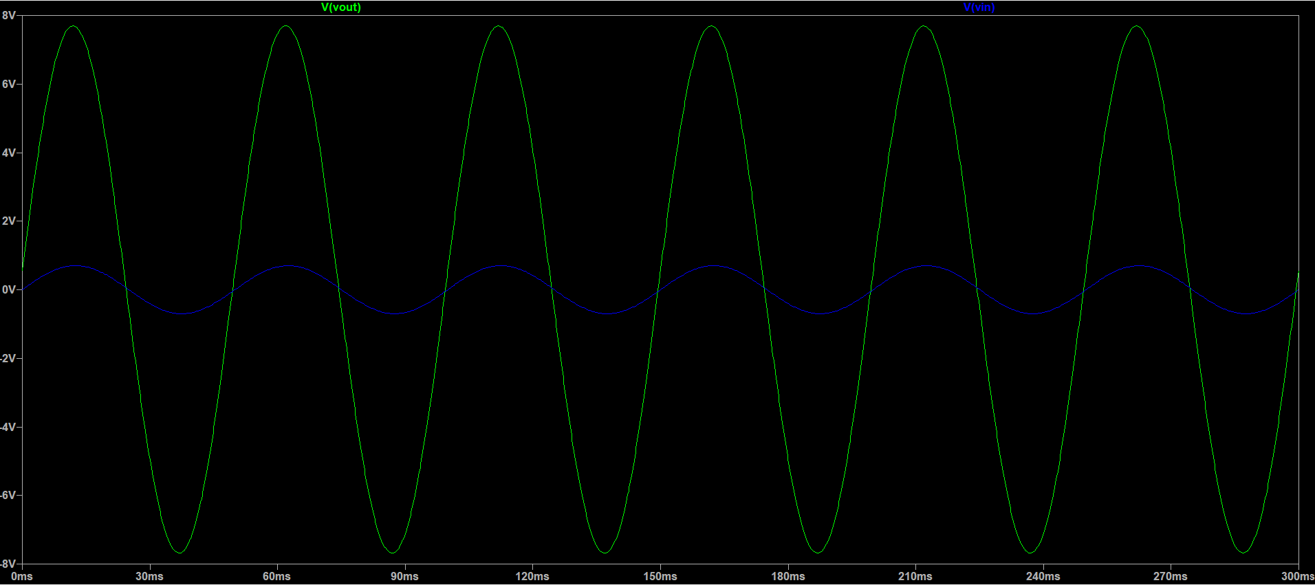
The transient simulation compares the input signal $V_{in}$ with the output signal $V_{out}$.
The output waveform demonstrates the amplifier's ability to reproduce the input sinusoid with increased amplitude. The region around the zero crossing is particularly relevant for evaluating crossover distortion in the Class-AB output stage.
2. Frequency Response
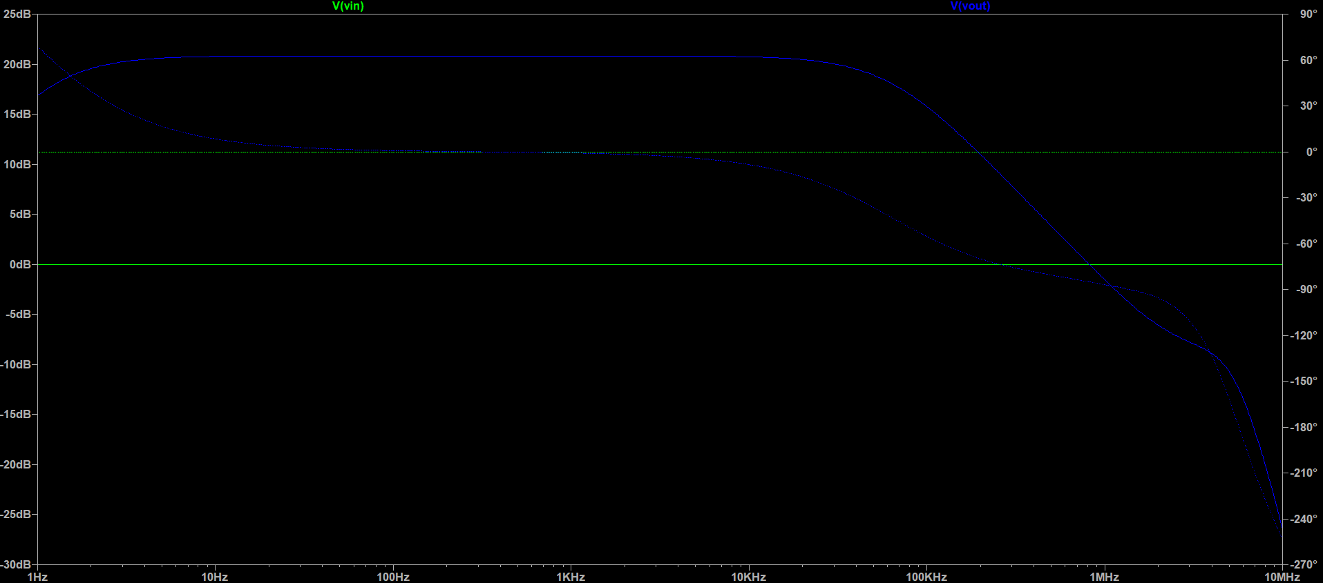
The Bode plot shows the output-to-input transfer function in terms of gain magnitude and phase.
The simulated response exhibits a relatively flat passband up to approximately 100 kHz, followed by high-frequency attenuation. The magnitude and phase responses provide insight into the amplifier's bandwidth and frequency-dependent behavior.
The voltage gain is set to the maximum value for this configuration, $A_v = 11 \simeq 20.8\text{dB}$.
3. Output Current Limiting
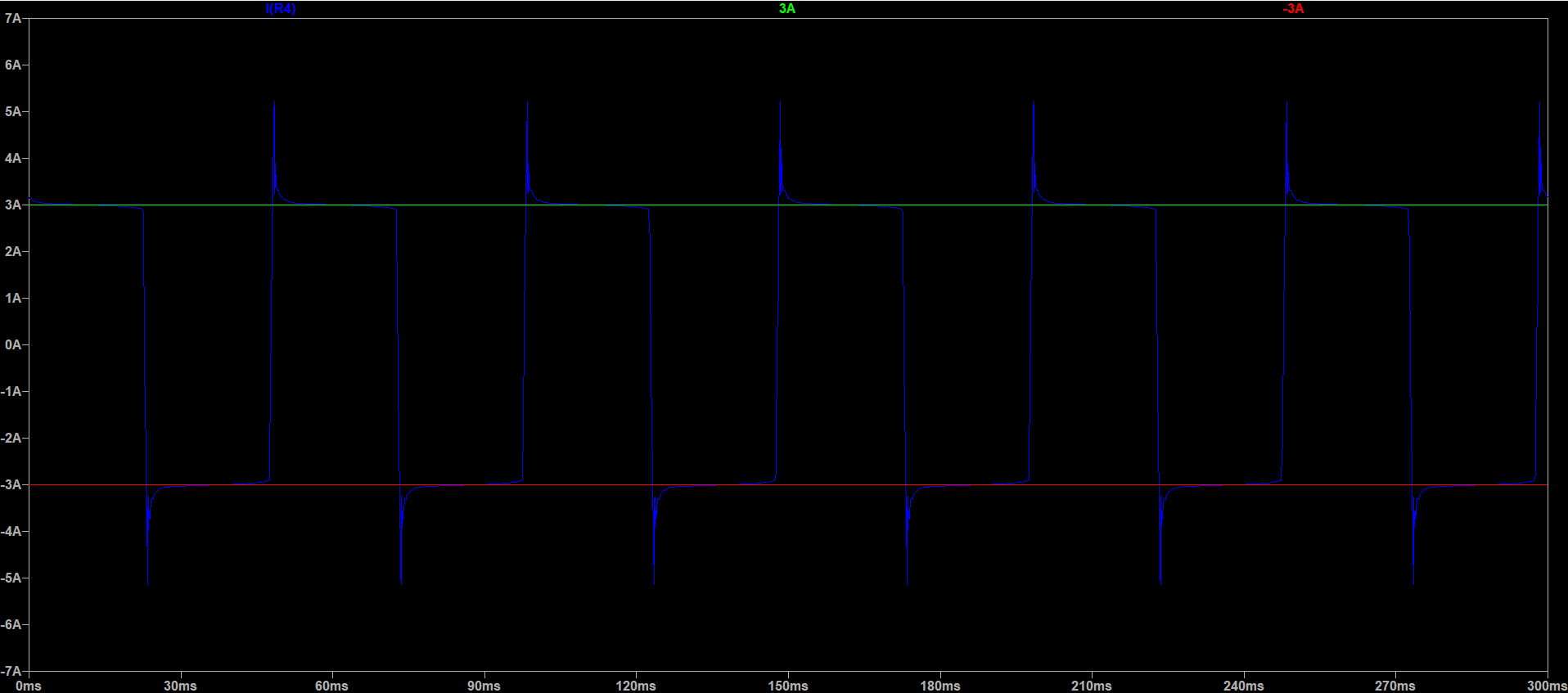
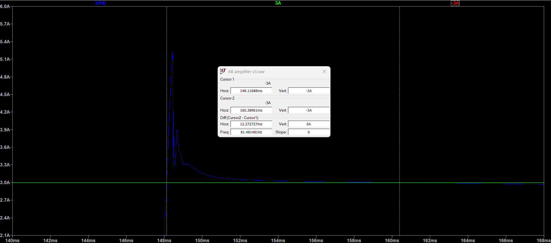
The current-limit simulation evaluates the behavior of the protection circuit under excessive output-current demand.
The circuit is designed to constrain the load current to approximately ±3 A, helping protect the output transistors against overload conditions.
4. Current-Limit Transient Response
A closer view of the transient response highlights the behavior of the protection circuit during a current-limit event.
The simulation shows the current transient settling toward the intended limiting level. The observed settling time is approximately 12 ms under the simulated conditions.
PCB Design
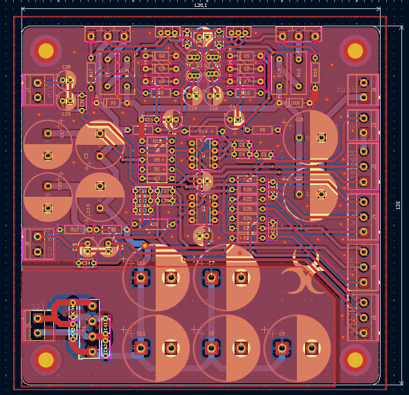
The PCB layout was developed in KiCad based on the Class-AB audio power amplifier schematic. Particular attention was paid to component placement, power-stage routing, and current-carrying traces to ensure reliable operation.
The PCB design aims to minimize unwanted parasitic effects and provide suitable routing for the relatively high currents handled by the output stage. The placement of the output transistors and current-sensing resistors is particularly important for thermal management and current-limit protection.
1. PCB Layout
The following image shows the PCB layout designed in KiCad, including component placement and routing.
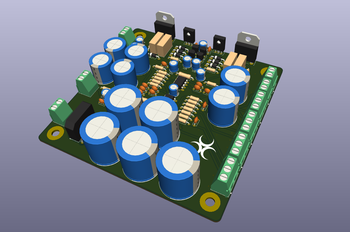
2. 3D PCB View
The 3D visualization provides a preview of the assembled PCB, showing the component placement and overall board layout. This view is useful for inspecting component positioning and evaluating the physical arrangement before manufacturing.
Repository Structure
text
.
├── README.md                               # Project documentation
├── img/                                    # Images and simulation results
├── KiCad/                                  # Schematics and PCB designs
│   └── mono_amplifier/
│       ├── AB_amp/                         # Class-AB amplifier design
│       ├── audio equalizer/                # Audio equalizer design
│       ├── mono_amplifier/                 # Main KiCad project — open this project only;
│       │                                   # the other designs are internally linked
│       └── power supply/                   # Power supply design
└── Spice/                                  # LTspice simulations
    └── opamp version/
        ├── AB amplifier final version.asc  # Final amplifier simulation
        ├── AB amplifier v1.asc             # Amplifier simulation, version 1
        ├── AB amplifier v2.asc             # Amplifier simulation, version 2
        └── AB amplifier v3.asc             # Amplifier simulation, version 3
Important: Open only the main KiCad project file: KiCad/mono_amplifier/mono_amplifier/mono_amplifier.kicad_pro. The other KiCad designs are internally linked to this project.
Progetto universitario per la realizzazione e simulazione di un Alimentatore da Banco Stabilizzato , completo di schemi elettrici KiCad, simulazioni LTspice, documentazione tecnica e file Gerber per la produzione del…
Este repositório apresenta os projetos desenvolvidos pelos estudantes da FEEC-UNICAMP na disciplina de graduação denominada Laboratório de Sistemas Embarcados.
Scripted analog EDA + PCB automation environment (KiCad 10 + ngspice + SKiDL) for macOS Apple Silicon
122 parts
Questions
How big is the Mono amplifier PCB?
It measures 120.1 × 120 mm and has 2 copper layers, 1.6 mm thick.
What parts does the Mono amplifier use?
97 parts, built around the TL081, BC327, BC337 and TIP3055. The full list of its parts is on this page, with links to each part's symbol and footprint where PCBKit's library has them.
Where can I download the Mono amplifier KiCad files?
From the dario0603/AB-class-amplifier repository on GitHub, at the commit this page was made from: the board is KiCad/mono_amplifier/mono_amplifier/mono_amplifier.kicad_pcb and its schematic KiCad/mono_amplifier/AB_amp/AB_amp.kicad_sch. PCBKit opens the board in the browser, with nothing to install.
Can I use the Mono amplifier design in my own project?
Its repository states no licence, so its author keeps all rights: ask dario0603 before reusing the design.