
2 layers105 × 75 mm

 daniestevez/ADF4158_PCB30
ADF4158 + HMC391 PCB for 10 GHz FMCW radar LO
ADF4158 PCB is an open-source printed circuit board by daniestevez, from the daniestevez/ADF4158_PCB repository on GitHub, published under the CERN-OHL-P-2.0 licence. It is a 4-layer board of 55 × 25 mm with 83 parts on 56 nets, routed with 358 tracks and 456 vias.
It is built around the HMC391LP4, AD8065ARZ and TPS62143RGT, with the ADF4158CCP, TLV74033PDBV and TLV74130PDBV among its other parts. Its parts include 33 resistors, 30 capacitors, 7 ICs, 3 connectors and 2 transistors.


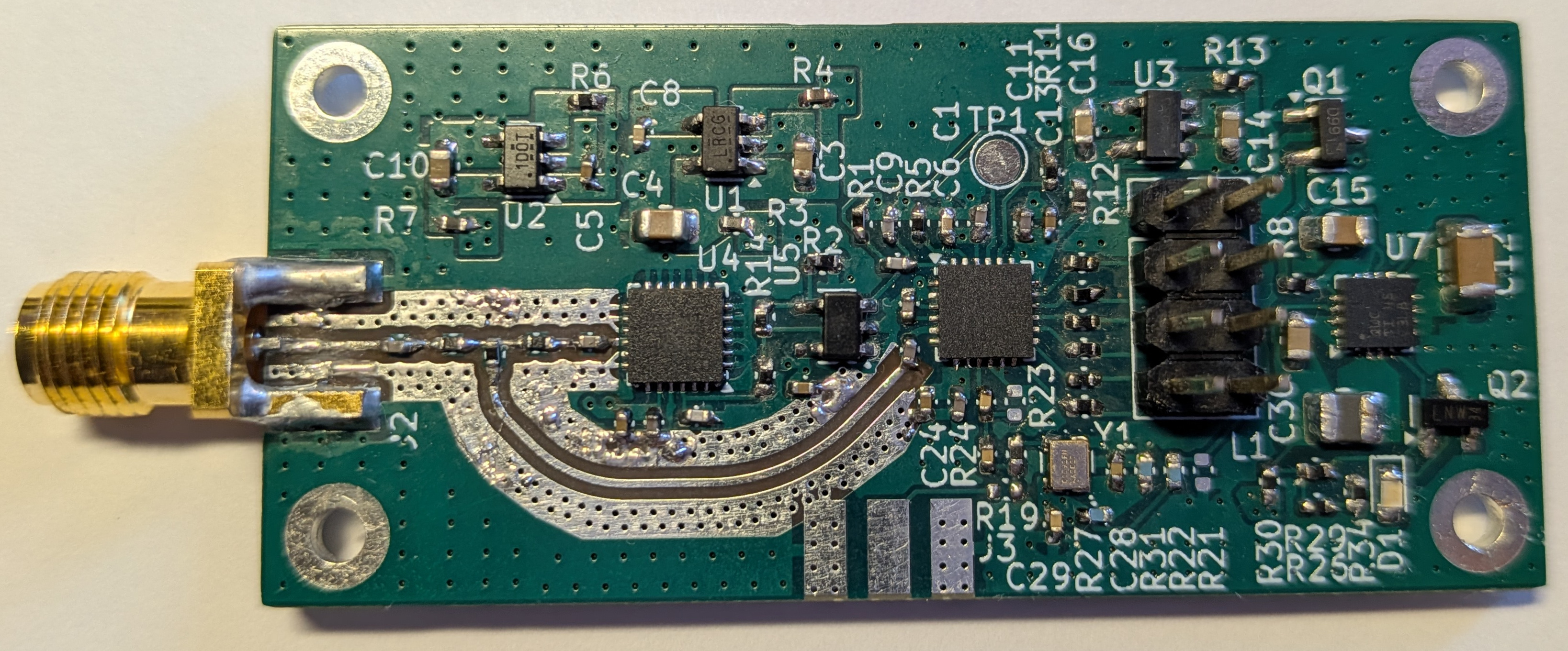
This project is a PCB that contains an ADF4158 direct modulation/waveform generating fractional-N frequency synthesizer and a HMC391 3.9 - 4.45 GHz VCO. The board is primarily intended as an LO source for a 10 GHz FMCW radar inspired by the ADALM-PHASER. The VCO output can be used with a subharmonic mixer and an IF around 1.6 GHz to cover the 10 - 10.5 GHz amateur radio band.
The board runs from a 12 - 16 VDC supply, exposes all the control pins of the ADF4158 in a 2.58 mm pin header (3.3V logic) and includes an optional 10 MHz reference input. The BOM cost is around 50€.
The PLL loop filter has been designed with ADIsimPLL. The design file is ADF4158_HMC391.pll.

Outputs for the latest commit in the main branch are built by CI and published
to Github pages. Additionally, outputs for each commit are published as a Github
artifact.
The BOM for this project is available as a DigiKey list. Note that this list includes DNP components such as the SMA connector for the external 10 MHz reference. You might want to exclude these components from your purchase.
The PCB is intended to be fabricated on JLCPCB using the following options:
These options are very inexpensive: $7.10 for qty. 5, $13.20 for qty. 10.
| Qty | Value | Footprint | References |
|---|---|---|---|
| 10 | 0 | Resistor_SMD:R_0402_1005Metric | R3, R4, R6, R7, R8, R12, R13, R19, R24, R30 |
| 8 | 330 | Resistor_SMD:R_0402_1005Metric | R9, R10, R25, R26, R28, R32, R33, R34 |
| 6 | 0.1u | Capacitor_SMD:C_0402_1005Metric | C5, C6, C13, C20, C22, C23 |
| 4 | 100p | Capacitor_SMD:C_0402_1005Metric | C2, C17, C19, C21 |
| 4 | 10k | Resistor_SMD:R_0402_1005Metric | R21, R22, R27, R31 |
| 4 | 10p | Capacitor_SMD:C_0402_1005Metric | C1, C11, C26, C27 |
| 4 | 1u | Capacitor_SMD:C_0603_1608Metric | C3, C10, C14, C16 |
| 4 | MountingHole | MountingHole:MountingHole_2.2mm_M2_Pad | H1, H2, H3, H4 |
| 3 | 10n | Capacitor_SMD:C_0402_1005Metric | C8, C28, C29 |
| 3 | 18 | Resistor_SMD:R_0402_1005Metric | R16, R18, R20 |
| 2 | 1k | Resistor_SMD:R_0402_1005Metric | R2, R17 |
| 2 | 1n | Capacitor_SMD:C_0402_1005Metric | C24, C25 |
| 2 | 5.1k | Resistor_SMD:R_0402_1005Metric | R1, R5 |
| 1 | 1.8k | Resistor_SMD:R_0402_1005Metric | R11 |
| 1 | 100k | Resistor_SMD:R_0402_1005Metric | R29 |
| 1 | 10u | Capacitor_SMD:C_0805_2012Metric | C15 |
| 1 | 2.2u | Inductor_SMD:L_1008_2520Metric | L1 |
| 1 | 22u | Capacitor_SMD:C_0603_1608Metric | C30 |
| 1 | 2N7002BK | Package_TO_SOT_SMD:SOT-23 | Q2 |
| 1 | 2k | Resistor_SMD:R_0402_1005Metric | R14 |
| 1 | 3.3u | Capacitor_SMD:C_1206_3216Metric | C12 |
| 1 | 390p | Capacitor_SMD:C_0402_1005Metric | C7 |
| 1 | 4.7u | Capacitor_SMD:C_0805_2012Metric | C4 |
| 1 | 51 | Resistor_SMD:R_0402_1005Metric | R23 |
| 1 | 56p | Capacitor_SMD:C_0402_1005Metric | C9 |
| 1 | 68p | Capacitor_SMD:C_0402_1005Metric | C18 |
| 1 | AD8065 | Package_TO_SOT_SMD:TSOT-23-5 | U5 |
| 1 | ADF4158 | Package_CSP:LFCSP-24-1EP_4x4mm_P0.5mm_EP2.5x2.5mm | U6 |
| 1 | Conn_02x04_Odd_Even | Connector_PinHeader_2.54mm:PinHeader_2x04_P2.54mm_Vertical | J1 |
| 1 | DMP3099L-13 | Package_TO_SOT_SMD:SOT-23-3 | Q1 |
| 1 | HMC391 | Package_DFN_QFN:QFN-24-1EP_4x4mm_P0.5mm_EP2.8x2.8mm | U4 |
| 1 | KT2016K | ADF4158_HMC391_PCB:KT2016K | Y1 |
| 1 | LED | LED_SMD:LED_0603_1608Metric | D1 |
| 1 | LP2985-10.0 | Package_TO_SOT_SMD:SOT-23-5 | U1 |
| 1 | SMA | ADF4158_HMC391_PCB:2484637-1 | J2 |
| 1 | SMA | ADF4158_HMC391_PCB:WRL-23187 | J3 |
| 1 | TLV74033P | Package_TO_SOT_SMD:SOT-23-5 | U3 |
| 1 | TLV74130P | Package_TO_SOT_SMD:SOT-23-5 | U2 |
| 1 | TPS62143 | Package_DFN_QFN:VQFN-16-1EP_3x3mm_P0.5mm_EP1.68x1.68mm | U7 |
| 1 | TestPoint | TestPoint:TestPoint_Pad_D2.0mm | TP1 |


shimotoriharuki/2021RoboTrace_Kicad
This repository contains circuit data for line-following robot (UnderBird).


MicroLind-Developers/microlind-hw
Hardware repository for the microlind project


ckflight/FMCW-RADAR
Frequency Modulated Continuous Wave Radar hardware and software design files with 26 dBm output power covering around 250 m.

Roshan-khatri78/Electronics-Projects-KiCad-
A collection of my KiCad projects and PCB designs. These projects reflect my learning journey in electronics and PCB design.
It measures 55 × 25 mm and has 4 copper layers, 1.62 mm thick.
83 parts, built around the HMC391LP4, AD8065ARZ, TPS62143RGT and ADF4158CCP. The full list of its parts is on this page, with links to each part's symbol and footprint where PCBKit's library has them.
From the daniestevez/ADF4158_PCB repository on GitHub, at the commit this page was made from: the board is ADF4158_PCB.kicad_pcb and its schematic ADF4158_PCB.kicad_sch. PCBKit opens the board in the browser, with nothing to install.
Its repository publishes it under the CERN-OHL-P-2.0 licence: you may reuse it on that licence's terms (keep the author's notice, and for a copyleft licence share your changes alike).