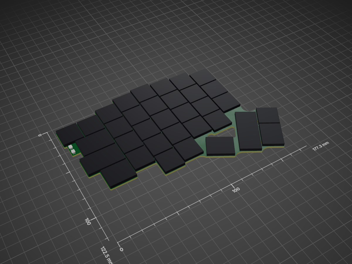
2 layers133 × 114.7 mm
 ctrlShiftBryan/ogre-mono
Inventory of the Ogre keyboard repos plus KLE layout export
Left placed is an open-source printed circuit board by ctrlShiftBryan, from the ctrlShiftBryan/ogre-mono repository on GitHub. It is a 2-layer board of 177.3 × 122.5 mm with 130 parts on 68 nets.
It is built around the E73-2G4M08S1C, XC6220B331MR-G and 1N4148W, with the CPG151101S11 among its other parts. Its parts include 36 diodes, 36 switches, 11 capacitors, 5 resistors and 3 connectors.


Not yet the design: config.yaml still places the parts as before. This is a
proposal to review in KiCad before it's carried into the config.
left-placed.kicad_pcb: every part placed, unrouted. The module's matrix
pins are reassigned onto its outer-row pads (col0-col6 on 10 9 7 6 4 3 1,
row0 17, row1 35, row2 15, row3 8, row4 2), J1 sits under Q and J2 under A
with their plugs entering sideways, and the support parts cluster at their
pins around the module.left-trial.kicad_pcb: the same board autorouted in one throwaway pass
(every net but GND): 0 unrouted, 93 vias, 1 DRC nit. A check that the
placement routes, not routing to keep.place.py made the placement from the build's board (greedy, each part at
the free spot nearest what it connects to); trial.py made the trial route.| Qty | Value | Footprint | References |
|---|---|---|---|
| 34 | ogre:CherryMX_Hotswap | MX1, MX2, MX10, MX11, MX12, MX13, MX14, MX15, MX16, MX17, MX18, MX19, MX20, MX21, MX22, MX23 +18 | |
| 34 | 1N4148W | ogre:Socket_Diode | D1, D2, D10, D11, D12, D13, D14, D15, D16, D17, D18, D19, D20, D21, D22, D23 +18 |
| 34 | CPG151101S11 | ogre:Hotswap_Socket | S1, S2, S10, S11, S12, S13, S14, S15, S16, S17, S18, S19, S20, S21, S22, S23 +18 |
| 6 | 4.7uF | ogre:C_0603 | C1, C3, C4, C8, C9, C11 |
| 2 | 10k | ogre:R_0603 | R3, R4 |
| 2 | 12pF | ogre:C_0603 | C5, C6 |
| 2 | 1k | ogre:R_0603 | R1, R2 |
| 1 | 100nF | ogre:C_0603 | C2 |
| 1 | 10M | ogre:R_0603 | R5 |
| 1 | 10uF | ogre:C_0603 | C10 |
| 1 | 10uH | ogre:L_0805 | L1 |
| 1 | 1uF | ogre:C_0603 | C7 |
| 1 | 32.768kHz | ogre:Crystal_FC-135 | Y1 |
| 1 | BAT | ogre:JST_PH_S2B-PH-SM4 | J2 |
| 1 | BQ24075RGTR | ogre:BQ24075 | IC1 |
| 1 | CHARGE | ogre:LED_3mm | LED2 |
| 1 | E73-2G4M08S1C | ogre:E73-2G4M08S1C | MCU1 |
| 1 | POWER | ogre:SW_SPDT_MSK12C02 | SW2 |
| 1 | RESET | ogre:SW_Reset_TS1187A | SW1 |
| 1 | STATUS | ogre:LED_3mm | LED1 |
| 1 | SWD | ogre:SWD_TC2030-NL | J3 |
| 1 | USB | ogre:USB_PicoEZmate | J1 |
| 1 | XC6220B331MR-G | ogre:XC6220 | IC2 |
It measures 177.3 × 122.5 mm and has 2 copper layers, 1.6 mm thick.
130 parts, built around the E73-2G4M08S1C, XC6220B331MR-G, 1N4148W and CPG151101S11. The full list of its parts is on this page, with links to each part's symbol and footprint where PCBKit's library has them.
From the ctrlShiftBryan/ogre-mono repository on GitHub, at the commit this page was made from: the board is ergogen/routing/proposal/left-placed.kicad_pcb. PCBKit opens the board in the browser, with nothing to install.
Its repository states no licence, so its author keeps all rights: ask ctrlShiftBryan before reusing the design.


ericrlau/NumDisciplineBLE
BLE Breakout Board To Replace ATMega Used In NumDiscipline

avlyubimov/svc-platform
Status: EVT-LAYOUT-AUTHORIZED; connectivity routing complete; fab review open


Cimos/etchy
Fast, trustworthy PCB visual and geometric diff tool (Rust). Successor to gerber-diff.