2 layers120 × 60 mm
Power module skiff
dwmorrin/power-module-skiff
This is a medium sized power module for $\pm$12 V and +5 V.
55 parts
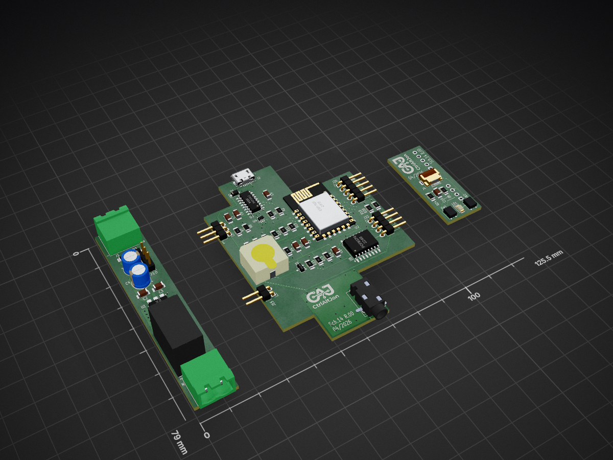
 CtrlAltJon/PeterThePowerMeter1
IoT Power Meter for real-time energy monitoring. Includes a local color display, acoustic alarms, and a web interface for smart home integration (Home Assistant/MQTT).
PeterThePowerMeter is an open-source printed circuit board by CtrlAltJon, from the CtrlAltJon/PeterThePowerMeter repository on GitHub, published under the MIT licence. It is a 2-layer board of 125.5 × 79 mm with 79 parts on 79 nets, routed with 487 tracks and 110 vias.
It is built around the CH340C, ESP-12F and ADS1115IDGS, with the PCF8574T, LD1117S33TR(MS) and UMH3NFHATN among its other parts. Its parts include 30 resistors, 15 capacitors, 13 connectors, 6 ICs and 3 diodes. It belongs with the home automation and IoT and sensors and measurement boards and the ESP8266 boards of this library.


[!CAUTION]
⚠️ IMPORTANT SAFETY WARNING & DISCLAIMER
THIS PROJECT INVOLVES WORKING WITH HIGH VOLTAGE (230VAC). HIGH VOLTAGE CAN CAUSE SEVERE INJURY, ELECTROCUTION, OR DEATH. FIRE HAZARD IS ALSO PRESENT.
This project is provided "as is", for educational and hobbyist purposes only. By using any part of this project (including hardware designs, PCB layouts, and software), you acknowledge and agree to the following:
- Assumption of Risk: You are solely responsible for your own safety and for any damage caused by the assembly, testing, or use of this device.
- No Liability: The author(s) shall not be held liable for any direct or indirect damages, including but not limited to: hardware failure, data loss, property damage (fire, short circuits), personal injury, or death, resulting from the use or misuse of this project.
- Assembly & Modification: Any errors in assembly, soldering (e.g., solder bridges), component selection, firmware modification or others actions are the sole responsibility of the user.
- No Warranty: There is no guarantee regarding the accuracy of measurements, the stability of the software, or the safety of the hardware design for long-term use.
- Local Standards: It is the user's responsibility to ensure that the device complies with local electrical codes and safety regulations.
IF YOU ARE NOT EXPERIENCED IN WORKING WITH MAINS VOLTAGE, DO NOT ATTEMPT TO BUILD THIS PROJECT.
This project is a Digital Power Meter designed for real-time energy monitoring with acoustic alarm when a threshold is exceeded. The system is engineered to fit within a standard 1-module DIN rail enclosure (roughly the size of a standard miniature circuit breaker), making it ideal for integration into domestic electrical panels.
Note: At the moment, the 3D design/CAD file for the DIN enclosure is not available. Contributions regarding the design of a suitable enclosure are highly welcome and would be a valuable addition to this project.
The system architecture is based on the ESP8266 (ESP-12F) microcontroller, leveraging its Wi-Fi capabilities for IoT integration and an ADS1115 to read voltage and current. For system health, an onboard TFPT1206L1002DV temperature sensor is included to monitor the internal thermal conditions of the enclosure.
For local interaction, the device features a 0.96" color LCD display that provides real-time data visualization and configuration menus. Users can navigate through multiple data pages and perform basic setup tasks using a multi-function physical button. Additionally, the system hosts a built-in Web Server, allowing for advanced remote configuration, firmware updates (OTA), and detailed system management via an intuitive Web UI.
The measurement stage utilizes two primary sensors:
Both sensors provide a 1VAC sinusoidal output. These signals are conditioned via a voltage divider network and sampled by an ADS1115 16-bit ADC, which communicates with the MCU via the I2C protocol.

To optimize GPIO usage, a PCF8574 I/O expander is employed for digital signal management and future use. The user interface consists of:
The device supports 2 power input options and 1 input 230VAC for Voltage reading:
[!CAUTION] No reverse polarity protection: This input currently lacks reverse polarity protection; correct orientation is mandatory.

USB Connector (J2): For secondary power or debugging.
AC Voltage Input (J3): High-voltage input for the ZMPT107-1 transformer.

This device is specifically designed and calibrated for 230VAC/50Hz Phase-Neutral grids (Standard European Grid).
The firmware architecture features a built-in Web Server for real-time monitoring, local configuration, and connections management (Wi-Fi and MQTT). The device natively supports the MQTT protocol for a smart home integration with platforms such as Home Assistant.
Navigation is handled via the multi-function button (Short press: Page toggle | Long press: Confirm/Action).
The device features a responsive Web UI. Users can connect via browser to the device's IP (visible on LCD page 6).
ADS1115 I2C Address Selection: Hardware-defined through two "0-Ohm bridge" resistors: R16 and R17. Only one of these resistors must be populated at a time:
0x490x48 (Default).Safety Design: To prevent assembly errors, the PCB layout utilizes a shared common pad for both R16 and R17. This physical constraint makes it nearly impossible to populate both resistors simultaneously, effectively protecting the +3.3V rail from a direct short circuit to Ground. However, be careful when assembling.


Peter The Power Meter has an embedded firmware designed for real-time single-phase energy monitoring. The system samples AC voltage and current waveforms, calculates Root Mean Square (RMS) values and active power consumption, provides a multi-page visual interface on a TFT display, and integrates with home automation systems via the MQTT protocol.
The following constants define how the raw electrical signals from the sensors are translated into human-readable values (Amps, Volts, Watts).
I_RMS = V_ADC * FACTOR_A_V.FACTOR_A_V of 25.0f is set based on the characteristics of the SCT-013 current transformer.V_Grid = V_ADC * FACTOR_V_V.FACTOR_V_V of 246.0f is derived directly from the ratio of the primary resistance (246KΩ) to the burden resistance (1KΩ).ADS_GAIN (GAIN_TWO) sets the full-scale range to ±2.048V, with an ADS_MULTIPLIER of 0.0000625.PTC_AVG_SAMPLES) to stabilize the PTC sensor data; if the temperature exceeds TEMP_WARNING_THRESHOLD (45.0°C), the display text turns RED.| Constant | Default Value | Unit | Description |
|---|---|---|---|
| FACTOR_A_V | 25.0 | A/V | Ratio of Amps per Volt from the CT circuit. |
| FACTOR_V_V | 246.0 | V/V | Ratio of Grid Volts per Volt from the VT circuit. |
| ADS_GAIN | GAIN_TWO | - | Sets ADC input range to ±2.048V. |
| ADS_SPS | 860 | Hz | Samples taken per second from the AC wave. |
| CURRENT_NOISE_FLOOR | 0.002 | V | Minimum voltage to consider a valid current reading. |
| VOLTAGE_MIN_THRESHOLD | 50.0 | V | Voltage below which the system uses a fallback value. |
These constants define the acceptable range and default values for the calibration parameters stored in EEPROM.
CAL_SCALE_DEFAULT is 1.0f (no correction), with a range between 0.1f and 10.0f.| Constant | Default/Range | Unit | Description |
|---|---|---|---|
| CAL_SCALE_DEFAULT | 1.0f | - | Default multiplicative scale factor. |
| CAL_SCALE_MIN | 0.1f | - | Minimum allowed value for scale factors. |
| CAL_SCALE_MAX | 10.0f | - | Maximum allowed value for scale factors. |
| CAL_OFFSET_V_MIN | -500.0f | V | Minimum allowed voltage offset. |
| CAL_OFFSET_V_MAX | 500.0f | V | Maximum allowed voltage offset. |
| CAL_OFFSET_A_MIN | -100.0f | A | Minimum allowed current offset. |
| CAL_OFFSET_A_MAX | 100.0f | A | Maximum allowed current offset. |
| CAL_OFFSET_TEMP_MIN | -50.0f | °C | Minimum allowed temperature offset. |
| CAL_OFFSET_TEMP_MAX | 50.0f | °C | Maximum allowed temperature offset. |
The device monitors internal temperature using the TFPT1206 series PTC sensor.
PTC_R_DIVIDER_TOTAL and PTC_R_DIVIDER_LOAD compensate for the voltage divider on the ESP8266 ADC input stage.PTC_NOMINAL_RES (10,000 Ω at 25°C) and PTC_COEFF (0.00411) define the resistance-to-temperature curve.| Constant | Default Value | Unit | Description |
|---|---|---|---|
| PTC_V_SOURCE | 3.3 | V | Logic source voltage for the sensing branch. |
| PTC_R_PULLUP | 33,000 | Ω | Fixed pull-up resistor ($R_7$) in the divider. |
| PTC_NOMINAL_RES | 10,000 | Ω | PTC resistance at 25°C. |
| PTC_COEFF | 0.00411 | - | TCR (Temperature Coefficient) of the sensor. |
| PTC_R_DIVIDER_TOTAL | 100,220 | Ω | ADC input stage total resistance ($R_{21} + R_{22}$). |
Contributions, issues, and feature requests are welcome! Feel free to open an issue or submit a pull request.
I am currently in the process of refining and cleaning up the firmware comments to ensure the code is as clear and readable as possible, even though the project is fully functional. I am also polishing the documentation and preparing additional guides that I'll upload to the repository soon. Currently seeking help with:
This project is licensed under the MIT License. See the LICENSE file for details.
CtrlAltJon
| Qty | Value | Footprint | References |
|---|---|---|---|
| 14 | 10K | Resistor_SMD:R_1206_3216Metric_Pad1.30x1.75mm_HandSolder | R3, R6, R9, R10, R11, R12, R13, R14, R15, R18, R19, R20, R31, R32 |
| 7 | 100nF | Capacitor_SMD:C_1206_3216Metric_Pad1.33x1.80mm_HandSolder | C2, C3, C5, C8, C9, C11, C14 |
| 4 | 10uF | Capacitor_SMD:C_1206_3216Metric_Pad1.33x1.80mm_HandSolder | C7, C12, C13, C15 |
| 3 | 82K | Resistor_SMD:R_1206_3216Metric_Pad1.30x1.75mm_HandSolder | R28, R29, R30 |
| 3 | Logo_CtrlAltJon | My_Lybrary_Footprint:Logo_CtrlAltJon | LOGO1, LOGO2, LOGO3 |
| 2 | 0 | Resistor_SMD:R_1206_3216Metric_Pad1.30x1.75mm_HandSolder | R16, R17 |
| 2 | 1K | Resistor_SMD:R_1206_3216Metric_Pad1.30x1.75mm_HandSolder | R23, R33 |
| 2 | 22uF | Capacitor_SMD:C_1206_3216Metric_Pad1.33x1.80mm_HandSolder | C6, C10 |
| 2 | 470R | Resistor_SMD:R_1206_3216Metric_Pad1.30x1.75mm_HandSolder | R1, R2 |
| 2 | PMEG2010AEH-115 | Diode_SMD:D_SOD-123F | D1, D2 |
| 2 | Screw_Terminal_01x02 | Connector_Phoenix_MSTB:PhoenixContact_MSTBA_2,5_2-G_1x02_P5.00mm_Horizontal | J1, J3 |
| 1 | 100K | Resistor_SMD:R_1206_3216Metric_Pad1.30x1.75mm_HandSolder | R22 |
| 1 | 100R | Resistor_SMD:R_1206_3216Metric_Pad1.30x1.75mm_HandSolder | R5 |
| 1 | 100uF | Capacitor_THT:CP_Radial_D6.3mm_P2.50mm | C4 |
| 1 | 120 | Resistor_SMD:R_1206_3216Metric_Pad1.30x1.75mm_HandSolder | R24 |
| 1 | 1N4007W | Diode_SMD:D_SOD-123 | D3 |
| 1 | 220R | Resistor_SMD:R_1206_3216Metric_Pad1.30x1.75mm_HandSolder | R21 |
| 1 | 3.2x4.2 | Button_Switch_SMD:SW_Push_1P1T_NO_Vertical_Wuerth_434133025816 | SW1 |
| 1 | 330R | Resistor_SMD:R_1206_3216Metric_Pad1.30x1.75mm_HandSolder | R4 |
| 1 | 33K | Resistor_SMD:R_1206_3216Metric_Pad1.30x1.75mm_HandSolder | R7 |
| 1 | 434133025816 | Button_Switch_SMD:SW_Push_1P1T_NO_Vertical_Wuerth_434133025816 | SW2 |
| 1 | 47uF | Capacitor_THT:CP_Radial_D6.3mm_P2.50mm | C1 |
| 1 | ADS1115IDGS | Package_SO:TSSOP-10_3x3mm_P0.5mm | U5 |
| 1 | BC807-40 | Package_TO_SOT_SMD:SOT-23 | Q1 |
| 1 | CH340C | Package_SO:SOIC-16_3.9x9.9mm_P1.27mm | U3 |
| 1 | Conn_01x02_Pin | Connector_PinHeader_2.54mm:PinHeader_1x02_P2.54mm_Vertical | J14 |
| 1 | Conn_01x02_Pin | Connector_PinHeader_2.54mm:PinHeader_1x02_P2.54mm_Horizontal | J15 |
| 1 | Conn_01x03_Pin | Connector_PinHeader_2.54mm:PinHeader_1x03_P2.54mm_Horizontal | J11 |
| 1 | Conn_01x03_Pin | Connector_PinHeader_2.54mm:PinHeader_1x03_P2.54mm_Vertical | J10 |
| 1 | Conn_01x04_Male | Connector_PinHeader_2.54mm:PinHeader_1x04_P2.54mm_Horizontal | J22 |
| 1 | Conn_01x04_Male | Connector_PinHeader_2.54mm:PinHeader_1x04_P2.54mm_Vertical | J23 |
| 1 | Conn_01x05_Pin | Connector_PinHeader_2.54mm:PinHeader_1x05_P2.54mm_Horizontal | J20 |
| 1 | Conn_01x05_Pin | Connector_PinHeader_2.54mm:PinHeader_1x05_P2.54mm_Vertical | J21 |
| 1 | Conn_01x08_Socket | Connector_FFC-FPC:Hirose_FH12-8S-0.5SH_1x08-1MP_P0.50mm_Horizontal | J4 |
| 1 | ESP-12F | RF_Module:ESP-12E | U2 |
| 1 | LD1117S33TR | Package_TO_SOT_SMD:SOT-223-3_TabPin2 | U1 |
| 1 | LED | LED_SMD:LED_1206_3216Metric | LD1 |
| 1 | MF-NSMF050-2 | Resistor_SMD:R_1206_3216Metric_Pad1.30x1.75mm_HandSolder | TH1 |
| 1 | MH3261-601Y | Inductor_SMD:L_1206_3216Metric | FB1 |
| 1 | PCF8574 | Package_SO:SOIC-16W_7.5x10.3mm_P1.27mm | U6 |
| 1 | PJ320E | Connector_Audio:Jack_3.5mm_PJ320E_Horizontal | J5 |
| 1 | SMD9650-DC3V | Buzzer_Beeper:Buzzer_CUI_CPT-9019S-SMT | BZ1 |
| 1 | Schurter UMT250 3403.0160.24 | Fuse:Fuse_Schurter_UMZ250 | F1 |
| 1 | TFPT1206L1002DV | Resistor_SMD:R_1206_3216Metric_Pad1.30x1.75mm_HandSolder | R8 |
| 1 | UMH3NFHATN | Package_TO_SOT_SMD:SOT-363_SC-70-6 | U4 |
| 1 | USB3076-30-A | Connector_USB:USB_Micro-B_GCT_USB3076-30-A | J2 |
| 1 | ZMPT107-1 | My_Lybrary_Footprint:Transformer_Zeming_ZMPT107 | TR1 |
It measures 125.5 × 79 mm and has 2 copper layers, 1.6 mm thick.
79 parts, built around the CH340C, ESP-12F, ADS1115IDGS and PCF8574T. The full list of its parts is on this page, with links to each part's symbol and footprint where PCBKit's library has them.
From the CtrlAltJon/PeterThePowerMeter repository on GitHub, at the commit this page was made from: the board is Hardware/source/KiCad/Archive/v00/PeterThePowerMeter.kicad_pcb and its schematic Hardware/source/KiCad/Archive/v00/PeterThePowerMeter.kicad_sch. PCBKit opens the board in the browser, with nothing to install.
Its repository publishes it under the MIT licence: you may reuse it on that licence's terms (keep the author's notice, and for a copyleft licence share your changes alike).
dwmorrin/power-module-skiff
This is a medium sized power module for $\pm$12 V and +5 V.


Hak4Kidz/H4K-cryptex
Cryptex virtual escape room badge for DC27 and our contribution to #badgelife.


jibrilsharafi/EnergyMe-Home
Smart energy meter capable of monitoring up to 16 channels. Supports MQTT, REST API, Modbus TCP, InfluxDB, AWS IoT Core. Friendly UI and fully open source (PCB, schematics, components, source code)


alejomancinelli/FCEIA_ProyectoFinal
Proyecto Final de Ing. Electrónica: Sistema de monitoreo de red eléctrica doméstica y/o industrial