

4 layers172 × 85 mm

 cr1tbit/laptop2usb
Zero-waste'ify your old-ass laptop powerbricks
Laptop2usb is an open-source printed circuit board by cr1tbit, from the cr1tbit/laptop2usb repository on GitHub. It is a 2-layer board of 135 × 42 mm with 44 parts on 27 nets, routed with 182 tracks and 15 vias.
It is built around the LM25085MY and SI7141DP. Its parts include 14 capacitors, 9 fuses, 8 connectors, 7 resistors and 3 diodes.
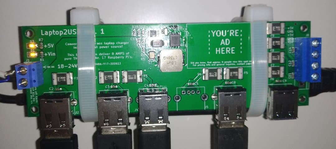
You fasten the PCB to a powerbrick.
The device takes anything between 17-20V, converts it into 5V, and splits into multiple USB and screw terminal ports. All of these ports are polyfuse-protected.
I'm yet to check a couple of things, and will do rev.2:
I ordered the prototype from JLCPcb, with passive elements surface mounted. Their online tool automatically assigns the elements from BOM into the part numbers from their store. Apparently it parsed the shunt 10mOhm resistor as 10 Mega Ohms.
With 10MegaOhms in the power path, the LM25085 somehow managed to produce 4V output with enough current to shine an onboard LED. Now that's dedication.
EDIT: it's been 2 years and one of my friends at work did literally the same kind of mistake when ordering PCBA from circuithub. I managed to catch that mistake quite fast, and implement a fix. I guess the lesson is, that those silly side-projects are really not in vain.
| Qty | Value | Footprint | References |
|---|---|---|---|
| 9 | 10u | Capacitor_SMD:C_0603_1608Metric_Pad1.05x0.95mm_HandSolder | C2, C3, C4, C5, C8, C9, C11, C12, C14 |
| 9 | Polyfuse_Small | Fuse:Fuse_2920_7451Metric_Pad2.10x5.45mm_HandSolder | F1, F2, F3, F4, F5, F6, F7, F8, F9 |
| 6 | USB_A | Connector_USB:USB_A_Molex_67643_Horizontal | J2, J3, J4, J5, J6, J7 |
| 2 | 10k | Resistor_SMD:R_0603_1608Metric_Pad1.05x0.95mm_HandSolder | R1, R5 |
| 2 | 3.32k | Resistor_SMD:R_0603_1608Metric_Pad1.05x0.95mm_HandSolder | R3, R6 |
| 2 | LED | LED_SMD:LED_1206_3216Metric_Pad1.42x1.75mm_HandSolder | D1, D3 |
| 1 | 1.8u | Inductor_SMD:L_Vishay_IHLP-4040 | L1 |
| 1 | 10m | Resistor_SMD:R_0805_2012Metric_Pad1.15x1.40mm_HandSolder | R4 |
| 1 | 1k | Resistor_SMD:R_0603_1608Metric_Pad1.05x0.95mm_HandSolder | R7 |
| 1 | 1n | Capacitor_SMD:C_0603_1608Metric_Pad1.05x0.95mm_HandSolder | C7 |
| 1 | 1u | Capacitor_SMD:C_0603_1608Metric_Pad1.05x0.95mm_HandSolder | C6 |
| 1 | 20.5k | Resistor_SMD:R_0603_1608Metric_Pad1.05x0.95mm_HandSolder | R2 |
| 1 | 390p | Capacitor_SMD:C_0603_1608Metric_Pad1.05x0.95mm_HandSolder | C10 |
| 1 | 4.7uF | Capacitor_SMD:C_0603_1608Metric_Pad1.05x0.95mm_HandSolder | C1 |
| 1 | 47uF | Capacitor_SMD:C_1210_3225Metric_Pad1.42x2.65mm_HandSolder | C13 |
| 1 | D_Schottky | Diode_SMD:D_SMB_Handsoldering | D2 |
| 1 | LM25085MY | Package_SO:MSOP-8-1EP_3x3mm_P0.65mm_EP1.73x1.85mm_ThermalVias | U1 |
| 1 | Screw_Terminal_01x02 | TerminalBlock:TerminalBlock_bornier-2_P5.08mm | J1 |
| 1 | Screw_Terminal_01x05 | TerminalBlock:TerminalBlock_bornier-5_P5.08mm | J8 |
| 1 | Si7141DP | Package_SO:PowerPAK_SO-8_Single | Q1 |

artificer123/Microwave_SDR_PCB
Collection of files used in development of a Xilinx Zynq based SDR with transverters for the V/UHF bands

aliihsan1913/Project-Ares
This repository contains the conceptual hardware design files for the high-power RF generator and the software source code for the simulation engine.


It measures 135 × 42 mm and has 2 copper layers, 1.6 mm thick.
44 parts, built around the LM25085MY and SI7141DP. The full list of its parts is on this page, with links to each part's symbol and footprint where PCBKit's library has them.
From the cr1tbit/laptop2usb repository on GitHub, at the commit this page was made from: the board is laptop2usb.kicad_pcb. PCBKit opens the board in the browser, with nothing to install.
Its repository states no licence, so its author keeps all rights: ask cr1tbit before reusing the design.