2 layers48 × 28 mm
Saihub prerouted
xqe2011/saihub
Give your agent a hand: MIT-licensed ESP32-C5 IO board that speaks MCP, so Cursor, Claude Code & Codex can drive GPIO, PWM, UART and power on real hardware.
57 parts4MIT

 Cptmeme/Nanoleaf-Shapes-controller3
Bus-powered half-duplex interface board between a 3.3 V MCU and the Nanoleaf Shapes panel bus
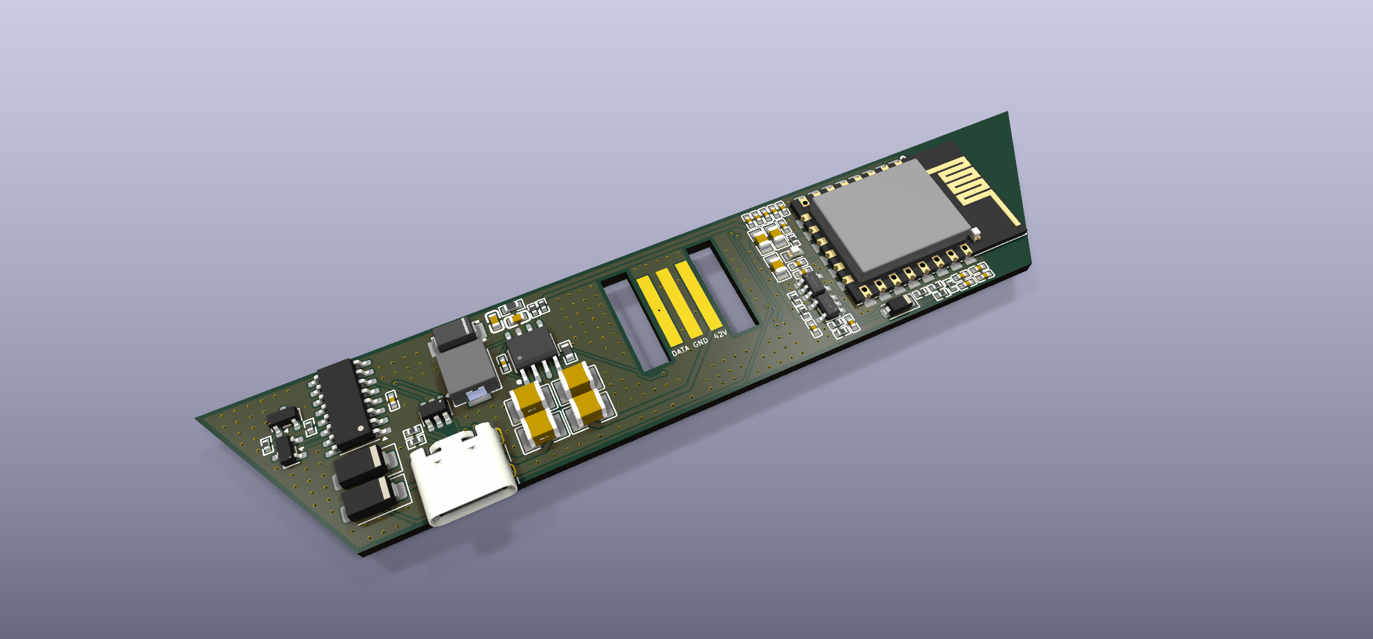
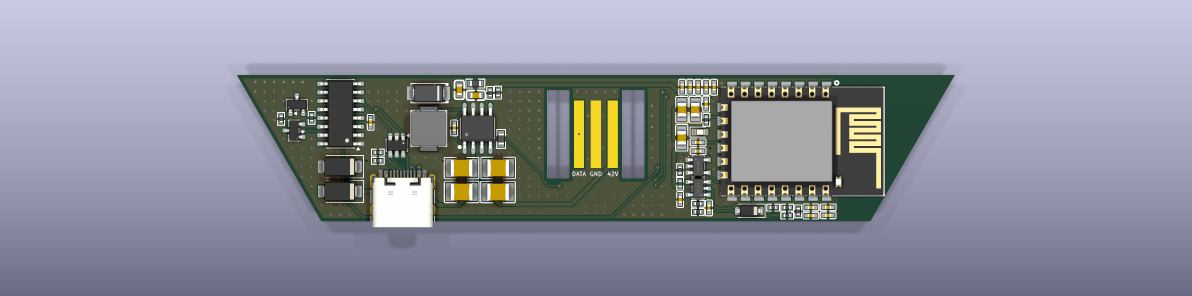
Nanoleaf shapes is an open-source printed circuit board by Cptmeme, from the Cptmeme/Nanoleaf-Shapes-controller repository on GitHub, published under the GPL-3.0 licence. It is a 2-layer board of 106.3 × 21.7 mm with 63 parts on 54 nets, routed with 368 tracks and 310 vias.
It is built around the 74LVC1G125GV, CH340C and ESPC5-12-H4, with the USBLC6-2SC6, TS-1187A-B-A-B and MMBT3904 among its other parts. Its parts include 25 capacitors, 17 resistors, 6 ICs, 5 diodes and 5 switches.


Rev B clips onto a panel like the stock controller, instead of connecting through a cut flex linker, and fixes the rev A issues. It replaced rev A in this folder on 2026-10-11. Rev A is still in the git history if you want it, at the commit before that change.
The KiCad files keep the name nanoleaf_shapes: the schematic stores its component references under that
project name, and renaming it would make KiCad drop every reference.
Not verified
No rev B board has been built or powered up. Boards are on order. Everything below is design intent and bench checking, not a working result.
What has actually been checked: DRC passes with 0 errors and 0 unconnected items, ground is one connected body, the enclosure clears the board in a 3D fit check against the KiCad component models, and the fabrication files were verified against the board they came from. None of that proves the circuit works.
The case is further from finished than the board, and it has never met a real PCB. Every fit check behind it is software against KiCad's 3D models, and those models have already been wrong three times in this project: U2's origin sits 3.9 mm off its own pads, the TS-1187A had no model at all until one was borrowed from another library, and a dozen footprints draw courtyards that leave their leads outside. A clearance that passes in software is a reasonable prior, not a measurement.
Specific things to expect trouble from on a first print:
- The snap fit interference, 0.15 mm, is a considered guess. Nobody has felt it.
SNAP_His the one number to change.- The button caps clear the switch plungers by 0.10 mm on datasheet geometry and 0.015 mm against the supplier's 3D model. That is tight enough that print tolerance decides it.
- Earlier versions of this case were printed and did reveal real problems, thin pocket walls among them. Assume this one has its own.
- Tolerances are tuned for an FDM printer with the author's settings and will not transfer unchanged.
Rev A, which is built and working, is in the git history and described in the top level README.
 |  |
| Mounting | Beside a panel, joined with a standard rigid Nanoleaf linker, like the stock controller |
| Panel contact | Three exposed PCB pads that the linker's spring contacts press on, inside a printed pocket |
| Programming | USB-C with a CH340C USB-serial chip and auto-reset. Data only: the board runs from the panels |
| Enclosure | FDM-printed. The linker pocket is designed from a linker model plus caliper measurements |
| Module | ESP-12F footprint kept, so the ESP32-C5 and ESP32-C6 modules (and others) still fit |
Both parts are verified on real panels, so they don't change:
Added after the first schematic pass:
C14996), from USB VBUS to the buck input. The TPS54360 runs from 4.5-60 V, so the
existing buck makes 3V3 from USB with no second regulator and no ORing logic: with a panel attached the node
sits at 42 V and the diode is reverse-biased, so nothing can reach the host; with no panel it conducts and
the buck runs from ~4.75 V. That leaves only ~0.25 V over the TPS54360's minimum, so a long thin cable under
load could drop it out -- fine for bench flashing at 100-300 mA, not guaranteed. Before this, flashing needed
a panel connected, because U5 runs off 3V3 and VBUS reached only U6.C47023097) to a 2.2 uF 100 V X7R 1210 (C5449052, the same part
as C1-C3). The 6.3 mm body stands 5.4-7.7 mm tall where the linker leaves 4.95. Four 2.2 uF in parallel give
~6 uF derated at 42 V against the TPS54360's 3 uF ceramic minimum. The electrolytic was also damping hot-plug
ringing; that is acceptable here only because a rigid linker's lead inductance is tens of nH.| # | Change | Why (what happened on rev A) | Parts |
|---|---|---|---|
| 1 | USB-C + CH340C with auto-reset | J2 has no GND and no reset or boot control, and an adapter's 3.3 V can't start the radios. Every serial flash needed BOOT + EN by hand, and several failed on loose wiring | USB-C receptacle (USB 2.0), CC1/CC2 5.1 kΩ to GND, CH340C (VCC = V3 = 3V3, 100 nF), 2 × NPN auto-reset (DTR/RTS → EN and the BOOT pad), ESD protection on D+/D− (USBLC6-2SC6) |
| 2 | 100 kΩ pull-up from COM to 3V3 | Without a panel, COM floats. On the ESP32-C5, bus RX is boot strap GPIO27, so download mode only worked with a panel attached. The first loopback frame without a panel also failed | 100 kΩ. U4 still pulls the far side down to about 0.07 V through R1 (2.2 kΩ) |
| 3 | 10 kΩ pull-up on module pad 11 | ESP32-C6 GPIO8 must be high for download mode; rev A leaves it floating | 10 kΩ. On the C5 this pad is GPIO15, which is neither a boot pin nor used by the flash, so the pull-up is harmless there |
| 4 | TVS on 42 V | The controller will be clipped onto live panels routinely. Hot-plugging into ceramic input capacitors can ring well above 42 V; the TPS54360 is rated 60 V (65 V absolute maximum). Keep C11: its ESR damps the ringing | SMAJ48A (48 V standoff) |
| 5 | Three contact pads instead of J1 | The pads replace the cut flex linker. HASL is fine -- an earlier note here called for ENIG, on reasoning that does not hold: HASL's ~10-25 um crown on a 1.50 mm pad is nothing against a spring finger's compliance, and the linker inserts, so the springs wipe the pads as they seat rather than pressing statically on tin oxide. ENIG's immersion gold is only ~0.05-0.1 um and wears through in a few dozen matings anyway; the finish for a mated contact is hard electroplated gold, which is a different and dearer process. If a board ever misbehaves, a burnish or a dab of contact enhancer costs a few euros. | Pads per Mechanical |
| 6 | D1 next to U1 | 16 mm on rev A, which enlarges the switching loop | Layout only |
| 7 | Status LED on module pad 18 | Shows pairing or Wi-Fi state. Optional | LED + resistor. Pad 18 is C5 GPIO8 / C6 GPIO19; neither is a boot pin |
| 8 | Test pads for COM, 3V3, GND, TX0, RX0 | Probing and a fallback serial connection | Pads only |
Dropped: reverse-polarity protection. The Nanoleaf connector only fits one way.
nanoleaf_shapes.kicad_sch has all the changes above. The rev A circuit is untouched, so the new parts sit in their
own block on the right of the sheet (now A3). Like the rest of the schematic, they connect through global labels.
| Refs | Part | Nets |
|---|---|---|
| J3 | USB-C receptacle (HRO TYPE-C-31-M-12 footprint) | USB_DP, USB_DN, USB_CC1, USB_CC2, USB_VBUS, GND; SBU not connected |
| R11, R12 | 5.1 kΩ | CC1, CC2 to GND (USB device) |
| U6 | USBLC6-2SC6 | ESD protection on D+/D−, referenced to USB_VBUS |
| U5, C22 | CH340C, 100 nF | VCC and V3 on 3V3; TXD → RX0, RXD ← TX0; ~DTR → DTR, ~RTS → RTS |
| Q1, Q2, R13, R14 | MMBT3904, 10 kΩ | Auto-reset as on Espressif's DevKitC: Q1 pulls BOOT (pad 12) low, Q2 pulls EN low |
| R15 | 100 kΩ | COM to 3V3 |
| R16 | 10 kΩ | PAD11 to 3V3 |
| D3 | SMAJ48A | 42V to GND, cathode on 42V |
| R17, D4 | 1 kΩ, 0603 LED | LED (pad 18) through the resistor to the LED, to GND |
| TP1, TP2 | Test pads | GND, COM |
| J1 | Linker pads | Footprint nanoleaf:Nanoleaf_Linker_Pads; 1 = 42 V, 2 = GND, 3 = COM, as before |
| J2 | Test pads | Footprint nanoleaf:TestPads_1x03_P2.54mm: RX0, TX0, 3V3 (with TP1 for GND) |
In the existing circuit: EN and BOOT labels on U2's pins (SW2 moved to the right to make room, same
connection), and pads 11 and 18 lost their no-connect flags.
Checked with kicad-cli 10.0.3: ERC gives 0 errors. The 33 warnings are all "Unspecified and Passive pins connected", because the easyeda2kicad symbols give their pins no electrical type; rev A has 30 of them. A netlist comparison with rev A shows every new net with exactly the intended pins, and every rev A connection intact.
Part numbers: the JLCPCB fields had copy-paste errors in rev A: J1 and U4 carried C1525 (the 100 nF
capacitor), J2 C52923, SW1 C5449052 and SW2 C4211. They didn't matter, because the rev A BOM file listed U3/U4
correctly and left the others out. Rev B fixes them: U1 C44377, U3/U4 C52140413 (from ../jlc_bom.csv), and no
number for J1, J2, SW1 and SW2 (not assembled). J1 and J2 are now marked "not in BOM". The new parts reuse the
design's numbers where the value already exists (10 kΩ C25744, 1 kΩ C11702, 100 nF C1525). The rest still need
picking at JLCPCB; commonly used ones to check stock against are CH340C C84681, USBLC6-2SC6 C7519, MMBT3904 C20526,
HRO TYPE-C-31-M-12 C165948, 5.1 kΩ 0402 C25905 and 100 kΩ 0402 C25741, plus an SMAJ48A and a 0603 LED.
USB ground: with USB connected, the computer's ground joins the panels' ground. That's fine as long as the Nanoleaf power supply's output is isolated, which is normal for a wall adapter; check it on the supply's label.
The KiCad footprint numbers the pads differently from the module datasheets. Footprint pads 1–8 are datasheet pins 1–8, pads 9–16 are pins 15–22, and pads 17–22 are pins 9–14 (the short end). Checked against the pad positions in the PCB and the pins verified on the ESP32-C5 board. Boot pins from ESP-IDF's GPIO tables: C5 GPIO2, 7, 25, 27, 28; C6 GPIO4, 5, 8, 9, 15.
| Footprint pad | Datasheet pin | ESPC5-12 (ESP32-C5) | WT0132C6-S5 (ESP32-C6) | Rev B use |
|---|---|---|---|---|
| 3 | 3 | EN | EN | EN, auto-reset |
| 8 | 8 | 3V3 | 3V3 | |
| 9 | 15 | GND | GND | |
| 10 | 16 | GPIO6 | GPIO7 | One-shot node (R10) |
| 11 | 17 | GPIO15 | GPIO8 (boot pin) | 10 kΩ pull-up |
| 12 | 18 | GPIO28 (boot pin) | GPIO9 (boot pin) | BOOT button, auto-reset |
| 13 | 19 | GPIO27 (boot pin) | GPIO10 | Bus RX |
| 14 | 20 | GPIO26 | GPIO3 | Bus TX |
| 15 | 21 | GPIO12 (U0RXD) | GPIO17 (U0RXD) | CH340C TXD |
| 16 | 22 | GPIO11 (U0TXD) | GPIO16 (U0TXD) | CH340C RXD |
| 17 | 9 | GPIO7 (boot pin) | GPIO18 | Free: avoid |
| 18 | 10 | GPIO8 | GPIO19 | Status LED |
| 19–20 | 11–12 | GPIO9, GPIO10 | GPIO20, GPIO21 | Free |
| 21–22 | 13–14 | GPIO13, GPIO14 (native USB) | GPIO22, GPIO23 | Free |
The ESP32-C5 module brings out native USB on pads 21–22, the C6 module doesn't. The CH340C works with both.
An upside-down isosceles trapezoid: the long parallel side is the joint edge, against the panel, and the
legs taper away from it at 60 deg. That is not a styling choice -- a hexagon's corner is 120 deg, so each leg
is the panel's own adjacent edge continued straight through its vertex. Carried to its end the two legs would
close into an equilateral triangle; this is that triangle cut off at CASE_DEPTH, which is the one dimension
free to grow for the electronics.
| Case | 113.00 mm on the joint edge, tapering to 74.89, 33.00 mm deep. The 113 sits just inside a hexagon's 114 mm edge, so the case never overhangs the panel it joins |
| Board | 106.30 -> 72.70 mm, 29.10 mm deep, 2605 mm2 |
| Joint edge | the case edge, not the board edge, is the datum for every linker dimension. The plate straddles it, 20.02 mm onto the panel and 20.02 onto the case, so this line has to fall halfway along the linker or it will not reach the panel. The board sits JOINT_INSET = 2.00 mm inside it, leaving a wall |
| Thickness | ~11 mm, against a panel's 6 mm (10 mm mounted). Forced, not chosen: the linker eats 4.95 mm from the back face down to the PCB surface before the 1.60 mm board. The controller stands proud |
Rev A's layout was discarded rather than extended, because its decoupling was in the wrong place -- all six 100 nF caps sat 8-14 mm from the module's 3V3 pin, in a tidy row, where trace inductance makes them useless, and the buck's catch diode was 17.9 mm from U1 with two of three input caps 12-15 mm from VIN.
| rev A | now | |
|---|---|---|
| Module 3V3 to nearest 100 nF | 8.17 mm | 1.93 mm (C5, C4, C6 within 3.7) |
| U1 VIN to nearest input cap | 4.36 mm | 2.51 mm |
| U1 SW to the catch diode | n/a | 3.03 mm |
| D1 ground to U1 ground | 17.89 mm | 9.80 mm |
Everything is on the front. Rev A had the module and both buttons on the back, which makes the board
double-sided to assemble; with all 60 parts on F.Cu, JLCPCB can build the whole thing, so a populated board is
an option rather than a hand-soldering job. The cost is that the buttons face the wall, which is tolerable --
they are flashing aids, and download replaces them anyway.
Flipping the module to the front mirrors it, so it is placed at rot 180: at rot 0 the antenna would point into the middle of the board and all seven signal pads would face the 3 mm strip under the joint edge. At 180 the antenna overhangs towards the right leg and the signals fan down into open board.
| Area | Holds |
|---|---|
| top right | the module, in the corner, with its antenna pointing out along the top edge and the board past it cleared of copper on both layers |
| above it | the 3V3 decoupling row and the enable network, sitting on the module's own pins |
| top left | the buck, shifted right to clear J3. The hot loop survived the shift: VIN to the nearest input cap 2.51 mm, SW to the catch diode 2.53 mm |
| centre | the bus buffers, with COM dropping straight into them from the linker above |
| left leg | USB. J3 rotated 300 deg so its mouth faces out of the 60 degree bevel, with U6's ESD clamp in the nearest free slot above it |
| bottom right | auto-reset, buttons, status LED and the serial pads, under the module they talk to |
Why the USB is on the leg, and what it cost. Putting it there frees the whole bottom edge for the five buttons. Every usable 16-pin USB-C footprint has four to six through-holes -- the only hole-free one in KiCad is a 6-pin power-only part -- and on the bottom edge those holes sat under the button row. On the leg they land at y 52.6..62.2, well clear of it.
The cost was repacking the buck: J3's rotated body reaches x 52.63, so D1, L1 and U1 all shifted right. The hot loop came through unchanged, but three things got worse:
The module's printed antenna is a keepout, x 118.0..126.4, y 48.8..67.0 (ANTENNA in board.py). It
overhangs the module's pads by 8.62 mm. Nothing is placed in it and the ground pour has a hole punched in its
polygon there -- a rule area would be the obvious way, but KiCad 10's ZONE_FILLER ignores those when driven
from Python.
The corner past the antenna is cleared too. That keepout only covers the antenna's own rectangle, and when the outline was widened to 106.3 mm the board grew out past it with the pour following -- 163 mm2 of board beyond x 126.4, 86% of it ground on both layers, reaching 13.6 mm into the direction the antenna radiates. A printed antenna needs the copper cleared where it radiates, not just underneath itself. That copper has since been removed: 0 mm2 on both layers beyond x 126.4, and no via is placed past x 121.2.
Width is not free: it is set by the hexagon's 114 mm edge, which the case has to sit inside. Depth is the only free dimension, so it is what sets the area. The first packed layout was 43.08 mm deep and only 37% of its front was covered in parts; at 33.00 it is 2605 mm2 against 3279, a 21% saving, with the front about half covered -- dense for two layers but still hand-routable.
What stops it going further: the module is 17.85 mm tall and J3 is 9.47 mm deep and has to reach the far edge, so 27 mm is about the floor, and at that depth the bottom band gets too tight for J3 plus the bus interface.
J2, rev A's RX0/TX0/3V3 header, is gone. The CH340C gives the same UART0 over USB with auto-reset on top,
and TP1/TP2 already cover scoping the bus, so it was dead weight. If the USB path ever needs bypassing, those
signals are still reachable at U5's pins.
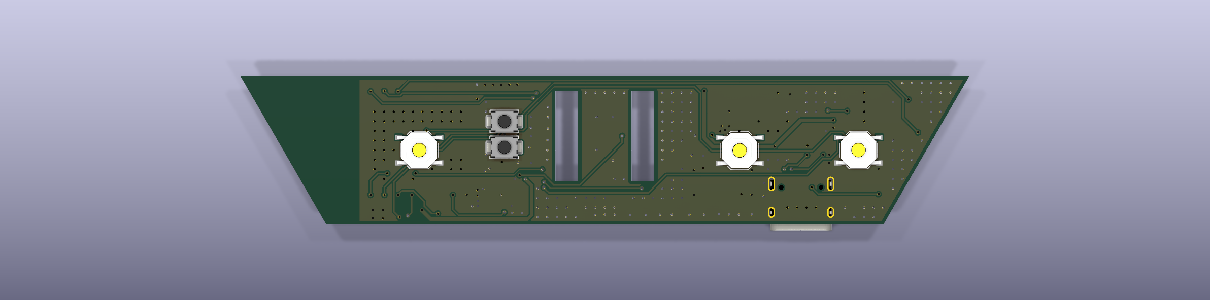
Five switches on the back, the room-facing side, so they can actually be pressed: three user buttons -- power, brightness up, effect -- plus reset and boot, moved across from the front, which had no room left for them and where they would have faced the wall anyway.
They sit on the board midline, y 56.825, and are centred on the two areas the linker cut-out leaves. The cut-out spans x 79.61..94.06, and at the midline the board runs x 39.93..133.74, so the areas either side of it are 39.676 mm wide each -- symmetric by construction:
| x | Where | |
|---|---|---|
SW3 BTN_PWR | 49.85 | left area, quarter point |
SW4 BTN_UP | 69.69 | left area, three-quarter point |
SW6 BTN_FX | 113.90 | right area, midpoint |
The left pair splits its area into four equal parts. SW6 is at its area's midpoint rather than a quarter point because the brightness-down button that shared that side was removed -- it sat over the module's printed antenna -- and FX moved to the middle of where the two had been.
Read from the back, the side being pressed, the mirroring puts them in the order effect, brightness +, power from left to right.
The user buttons are C&K PTS645, 6 x 6 mm with four gull-wing pads -- far easier to hand-solder than the two-pad parts, and a real MPN rather than a house number.
On switch size. A swap to a generic 6x6x5 SMD part was looked at and dropped: the PTS645 is a 6 x 6 mm part, so the land pattern would not shrink. Its 10.19 x 6.89 mm courtyard is simply what a 6 x 6 body with gull-wing leads needs, and Omron's B3S-1000 lands within 0.01 mm of it. The saving only arrives with a smaller body -- Alps SKQG or XKB TS-1187A, both 5.2 mm square, come in at 8.50 x 5.50 and 7.50 x 5.60 mm, about 40% less area, 85 mm2 across the three -- and TS-1187A goes to 5.0 mm height, so the tall button survives. Not done: the board is routed and DRC-clean, and 15 track ends land on these pads.
Reset and boot are not needed in normal use. The auto-reset circuit drives EN and BOOT from DTR/RTS, so
esptool handles both without anyone touching a button, and the firmware's download command covers it too.
They are kept for rev B purely as bring-up insurance: that circuit is new here and has never been tested, and
with J2 gone there is no other serial path if it misbehaves. Not the only fallback -- Q1's collector and an
EN-side pad can be shorted to TP1 with tweezers -- but a button beats tweezers on a first spin.
They cost no board area, since the back is otherwise empty, and they use the smaller 4-pad C&K KMR2 (5.69 x 3.69 mm courtyard against the PTS645's 10.19 x 6.89). Both sit just right of the linker cut-out at x ~101.5, under the module they talk to: SW2's nearest pad is 1.67 mm from the module's edge pads. Drop them in the next spin once auto-reset is proven, or mark them DNP now: the pads cost nothing and can be populated if the first boards misbehave.
The TPS54360 sheds its heat through its exposed pad, so that pad needs a path to the ground pour on the back. The easyeda2kicad footprint provided one: four plated holes inside the pad. Right idea, wrong place to put it.
Expressing them as footprint pads cost more than it bought. They carry no pad number, so no schematic
pin can match them -- four net_conflict parity warnings, and their GND net had to be set on the board by
hand rather than coming from the netlist, where an Update PCB from Schematic could quietly drop it again.
And a plated hole inside an SMD part's courtyard is exactly what pth_inside_courtyard looks for: two more
errors, against SW4 on the other side. The same library also gave them *.Cu *.Paste *.Mask, so they had
mask openings and paste apertures on both faces, leaving bare GND copper 0.271 mm from SW4's BTN_UP pad.
They are now ordinary GND vias on the board, placed by hand, and gone from both the board footprint and
the library copy (revb_drop_thermal_pads.py). Nothing is lost: same four holes, same 0.61 / 0.30 mm, same
net, same places, still inside the exposed pad's mask and paste window, and tented on the back by default.
Four warnings and two errors stop being asked about, and U1 matches its library again.
| via | x | y |
|---|---|---|
| 71.32 | 53.35 | |
| 72.32 | 53.35 | |
| 71.32 | 54.35 | |
| 72.32 | 54.35 |
What it costs: vias do not move with U1. That is precisely why the footprint author put them in the
footprint, and why KiCad's own SOIC-8-1EP_..._ThermalVias does the same. Fine while U1 is placed and
routed -- but if it ever moves, the vias stay behind and nothing warns you.
The exposed pad's own paste aperture is still a solid 2.00 x 2.00 mm, 100% coverage, where KiCad's equivalent splits it four ways at 65% and IPC-7093 wants roughly 50-80%. Unchanged and still open.
PCBWay has no parts library to browse -- that is the main difference. It sources globally by manufacturer part number through authorised distributors (Digi-Key, Mouser, Arrow, Avnet), with kitted, partial-turnkey and full-turnkey options, and quotes by hand rather than pricing instantly online. So:
C... numbers in the BOM mean nothing to PCBWay. The BOM needs designator, quantity, package
and manufacturer part number; for passives with no MPN, value and package are enough. No PDFs.To browse what is actually available, use a distributor rather than PCBWay: https://www.lcsc.com, https://www.digikey.com, https://www.mouser.com. Take the MPN from there.
| File | Contents |
|---|---|
mechanical/board.py | The outline, the joint datum and the linker keepouts; shared with the enclosure so the two cannot drift |
mechanical/revb_outline.py | Writes the outline, the linker pads, the ground pour and the escape tracks into the board |
mechanical/revb_place.py | Places all 60 parts and adds the 19 that were only ever in the schematic |
mechanical/revb_check.py | Clears stale routing and checks containment, courtyards, keepouts and decoupling distances |
mechanical/revb_place_rest.py | Places only the parked parts, and ties U1's thermal vias to GND |
mechanical/revb_centre_buttons.py | Centres the four buttons on the midline and on the quarter points either side of the linker |
mechanical/revb_stitch.py | Grid of ground stitching vias; dry run by default, --place to apply |
mechanical/revb_tent_thermal_vias.py | Checks and fixes U1's thermal vias -- copper-only layers in the easyeda2kicad library and on the board, plus their GND net and solid zone connection. Run it after any footprint or netlist update |
They all need KiCad's own Python, for pcbnew:
/Applications/KiCad/KiCad.app/Contents/Frameworks/Python.framework/Versions/3.9/bin/python3.
197 vias on the board, 168 of them GND. 43 came from revb_stitch.py, 0.6/0.3 mm, on a
3.0 mm grid centred on the board, so they fall in seven straight rows at
y 47.825 to 65.825 and in straight columns. revb_stitch.py generates the grid and then throws away every
point that would not be a good via. Of the 219 grid points that land on the board:
| Rejected for | Count |
|---|---|
| the pour only reaches one layer there, so the via would stitch nothing | 108 |
| the antenna keepout and the board beyond it | 27 |
| too close to a pad | 26 |
| the linker slots | 8 |
| the board edge | 6 |
| a non-GND track | 1 |
| kept | 43 |
The pour test is the one that matters: a candidate only survives if its whole 0.6 mm pad -- centre plus four edge probes -- sits inside the GND fill on both F.Cu and B.Cu. That is why the row at y 62.825 has only two vias: the button row blocks the back pour across the middle of the bottom edge.
Clearance to other copper is checked at 0.30 mm, three times the 0.1 mm netclass rule, so the grid keeps its margin even where the routing is tight. The script asserts that the track, footprint and zone counts are unchanged, and takes a timestamped backup, so it cannot disturb hand routing.
The re-routed board carries the real stitching. It was built in replan/ and promoted to
nanoleaf_shapes.kicad_pcb on 2026-10-10 once DRC came back clean, so replan/ is now a
superseded copy, since deleted. The board and schematic in hardware/ are the live ones. Pitch went from 3.0 mm to 1.4 mm after a
sweep (3.0 -> 42 vias, 2.5 -> 48, 2.2 -> 72, 2.0 -> 79, 1.8 -> 96, 1.6 -> 121, 1.4 -> 177), giving 15 rows
and 256 GND vias on the board as shipped: the grid contributed 177, revb_fix_islands.py added the two
that rescue stranded ground pins, one was dropped as too close to Q2, and the rest were placed by hand. Of 1005 grid points on the board:
| Rejected for | Count |
|---|---|
| the pour only reaches one layer there | 495 |
| the antenna keepout and the board beyond it | 124 |
| too close to a pad | 93 |
| the board edge | 66 |
| a non-GND track | 32 |
| the linker slots | 16 |
| hole to hole | 2 |
| kept | 177 |
The result is one connected body of ground copper, 2221 mm² over 16 islands on both layers, and DRC reports 0 errors and 0 unconnected items. What is left over is four fill artifacts at the zone boundary -- a 0.142 mm² hairline 0.01 mm wide and three zero-area specks -- all an order of magnitude below the 0.1 mm minimum feature any fab can etch, so no copper will actually exist there.
A grid alone was not enough. Two F.Cu pours stayed electrically separate, and each held a ground pin:
| Island | Area | Stranded pin |
|---|---|---|
| x 54.35..58.00, y 51.42..56.85 | 4.03 mm² | U6.2, GND of the USBLC6-2SC6 USB ESD array |
| x 99.61..101.24, y 59.81..62.14 | 2.07 mm² | U3.3, GND of the 74LVC1G125 data buffer |
U3.3 is the buffer's own ground, so the part would not have worked. Neither island took a grid via: island A's
grid points all fell inside SW3's pad keepout, and island B is boxed in so tightly by R1 and U4 that a
breadth-first path search found no escape on F.Cu at all -- not a 0.25 mm track, not even 0.12 mm at 0.15 mm
clearance. A via was the only way out of island B.
mechanical/revb_fix_islands.py places one standard 0.6/0.3 mm via at the widest point inside each island,
found by binary-searching the largest free disc with KiCad's own collision test. Two details matter:
pad_standoff keeps the via off pad copper so reflow cannot wick solder down the barrel. At 0.20 mm the
via lands 0.89 mm from U6.2 with 0.352 mm of clearance -- close enough to keep the ESD return path short.
Raising it to 0.40 mm buys nothing and forces the via into a 0.203 mm gap instead.Island B's via clears R1.1 by 0.205 mm against the board's 0.200 mm minimum. It passes, but it is the
tightest copper on the board; nudging R1 a tenth of a millimetre would make it comfortable.
The 1.4 mm grid dropped one via 0.131 mm from Q2 pad 3, under the 0.200 mm minimum. The test compared
against GetSize(), which is in the pad's own frame: Q2 sits at 90 deg, so its 1.475 x 0.600 mm pad read
as 0.600 x 1.475 and the via cleared on the y axis by arithmetic that described a pad in the wrong
orientation. The same code also filtered tracks on GetClass() == "PCB_TRACK", which skips PCB_ARC
entirely, and approximated every pad as a rectangle.
revb_stitch.py now asks KiCad instead -- GetEffectiveShape(layer).Collide(disc, clearance) -- which is
exact and covers rotation, roundrects, ovals, custom pad shapes and arcs for free. An audit of all 229 vias
with the exact test found exactly one violation, the Q2 one, and it is gone. The 24 vias sitting between
0.20 and 0.30 mm are all hand-placed and legal.
DRC: 0 errors, 0 unconnected items, 0 schematic-parity issues. 15 violations, all warnings, all cosmetic:
| 10 silkscreen | 7 silk_overlap, 2 silk_edge_clearance, 1 silk_over_copper. PCBWay clips silk off pads anyway. |
3x text_height | J1's DATA/GND/42V labels at 0.6 mm against a 0.8 mm rule. Deliberate -- they have to fit on the tongue. |
2x lib_footprint_mismatch | J3 and U5, both 1 nm rounding noise: a few line endpoints stored as 4.699999 where the library has 4.7. Pads, layers, shapes and polygons are identical. |
The errors that used to sit here are gone for three different reasons, worth keeping apart: the two
pth_inside_courtyard and the four net_conflict went when U1's thermal vias stopped being footprint
pads; the two clearance against the GND zone were a stale pour after a hand edit, cleared by a
refill, not by any geometry change; and U1 no longer differs from its library because the library was
corrected alongside it.
Board and schematic agree exactly: 63 symbol instances, 63 footprints, identical reference lists, and every footprint has all of its pads inside the outline. Nothing is parked off-board.
42 V creepage was re-checked after the netclass clearance was dropped to 0.1 mm: the tightest same-layer gap on the 42 V net is 0.200 mm, to C1 pad 2 on F.Cu. IPC-2221 wants 0.13 mm for 31-50 V under solder mask, so the lowered clearance has not compromised it.
From Christian Panton's write-up: the linker tabs carry the spring contacts, and the devices (panels, power supply, controller) only have exposed PCB pads, held in place by the moulded case. His pads measure about 10 × 1.5 mm with 1 mm gaps. The pad order is 42 V, GND, DATA, with GND in the middle.
From Nanoleaf Panel Connector by thegestalt, a printable contactless linker that clips into the panels. It is licensed CC BY-NC, so it's used here only as a dimensional reference: neither the STL nor a remix of it goes into this GPL-3.0 repository, and the pocket is modelled from the numbers below.
| Feature | Size |
|---|---|
| Base plate | 17.3 × 40.0 mm, 2.37 mm thick, 2.0 mm corner radius. It sits in a recess in each panel's back, flush |
| Plug, one per end | 11.4 mm wide × 12.5 mm long, 2.5 mm tall; the outer end is chamfered |
| Gap between the two plugs | 9.0 mm, so a pocket starts about 4.5 mm in from its panel's edge |
| Plug corners | 3.0 mm radius |
| Snap hooks | Two per plug, one on each side, 2.7 mm wide, centred along the plug (4.9–7.6 mm from either end) |
| Locating posts | Plain, non-grabbing posts beside the hooks, found on a real linker by the test print below. They need the PCB slot to run the plug's whole length, not just the hook band |
| Hook barbs | Stick out 0.41 mm past the plug sides, widest 3.08 mm below the plate's inner face, which is 0.6 mm below the plug top; hook tips reach 3.63 mm below it |
SLOT_OUT 1.20 mm, not BARB_OUT 0.41): the slot must never be what stops the barb springing,
and the width costs nothing out there. It does not set how hard the linker grips — that is
BARB_OUT - CLEAR, the barb's reach past the pocket wall's inner face, and the slot plays no part in it.| File | Contents |
|---|---|
mechanical/linker.py | Every linker and pad dimension, shared by the two scripts below |
mechanical/pocket_test.py → pocket_test.stl, pocket_test_{lower,upper}.stl (not committed, run the script) | Printable test piece: the plate recess, one pocket with a PCB-height floor, and the two slots. Written whole and split at the latch ledge; pass a clearance (python pocket_test.py 0.10) for a tighter-gripping variant, named _c010 |
mechanical/linker_footprint.py → nanoleaf.pretty/Nanoleaf_Linker_Pads.kicad_mod | KiCad footprint: the three pads (bare copper, no paste), the slots on Edge.Cuts, and a courtyard for the printed pocket walls. The project's fp-lib-table names the library nanoleaf |
Both scripts run with Python 3; the test piece also needs pip install manifold3d numpy. Checked in software
with the linker model sitting flush in the recess: the plate and plug touch nothing, and the barbs catch under
the pocket wall after 0.3 mm of pull.
Run python pocket_test.py to generate the STLs, which are not kept in the repository. Print the split
pair, pocket_test_lower.stl and pocket_test_upper.stl, both as they come, bottom on the bed, and stack them on the two 3 mm registration pins. Neither half has an overhang. pocket_test.stl is the
same block in one piece, for reference and for a resin or machined part — on FDM it prints the ledge the barb
catches as a cantilever reaching inward over the slot, so the latching corner is the droopiest point of an
overhang and rounds away. Then push one end of a real rigid linker in:
If the fit is tight or loose, or it seats without latching, change CLEAR — run python pocket_test.py 0.10 for
a variant. Clearance is the only lever on grip: tighter clearance, deeper grip, until the plug stops going in.
Result, 2026-10-03: the first print was cut only to the hook band (HOOK_Y), and the linker's plain locating
posts fouled the floor. The slots now span the plug (SLOT_Y in linker.py), which both the test piece and the
footprint follow. Still to measure on a panel PCB: how much wider than the hooks the real slots are.
Result, 2026-10-04: the linker seats fully and flush but does not latch. Two causes, both addressed, neither confirmed yet, as there are no calipers to hand:
BARB_OUT 0.41 and CLEAR 0.20 the grip was only 0.21 mm nominal, which FDM tolerance alone can
swallow. BARB_OUT came from the community model, which was already wrong about the locating posts, so it may
simply be larger in reality; the slot was widened outboard so that a larger barb is free to deploy.Next print: the split pair at the default clearance, then 0.10 if it still will not catch. If the tighter one
latches, the barb is real and the grip was the problem; if neither does, measure a real barb before changing
anything else.
Two printed parts: a tray the board drops into, and a lid carrying the three back buttons.
enclosure.py builds both, board_mock.py builds a printable stand-in for the assembled board, and both
read parts.json, which export_parts.py writes out of the board under KiCad's Python. So the case is
cut to the board KiCad actually has, not to a drawing of it.
Nothing in the thickness direction is a free choice until the board's back face. The linker fixes the
first three rows: the case edge has to fall halfway along the linker, and pocket_test.py proved the
recess and pocket against a real one.
| z | ||
|---|---|---|
| 0.00 | outer face, wall-facing | the linker plate recesses into this |
| 2.37 | plate recess floor | PLATE_T |
| 1.10 | component cavity ceiling | 3.85 mm clear, for J3's 3.50 |
| 4.95 | board, front surface | + PLUG_H 2.48 + TOP_GAP 0.10 |
| 6.55 | board, back surface | + BOARD_T 1.60 |
| 8.05 | top of the back parts | + 1.50, the user buttons |
| 8.40 | lid inner face, the seam | + BACK_GAP 0.35 |
| 10.00 | outer face, room-facing | + LID_T 1.60 |
Total 10.00 mm, and 11.00 mm across a button pad -- the same 1 cm as a panel. The board's front faces the wall, because that is the side the linker pads are on, which is what puts the buttons on the room side where they can be pressed.
One open cavity, not a pocket per part. The front of the board sits in open air. Giving each part its own pocket was tried and dropped: it makes a stiffer tray, but it wraps every part in plastic 0.25 mm away, and the buck has to shed its heat somewhere. 80% of the board's area is open to the cavity at the board plane.
What that costs is support, which comes back three ways. A 1.20 mm rim round the edge, opened up wherever a front part reaches into it. The plate region, solid under the recess except where a part needs the room. And eight 1.80 mm posts, 3.85 mm tall, out where the rim cannot reach -- chosen, not placed: parts, pocket and recess are subtracted from the interior, what is left is eroded by the post's own radius to give where a centre may sit, and candidates are picked greedily furthest-from-the-rest so they spread. They are small because the gaps between parts are a thin web rather than open blobs; at 3.00 mm only three places took one, at 1.80 mm eight do, from x 37.8 to x 135.8.
The linker pocket does not need the cavity filled to stop being an island -- it needs attaching. That
is the recess wall ring's second job: running it from the outer face up to Z_CAV_PLATE rather than
stopping at the recess floor, it overlaps the 1.10 mm floor below it and the recess floor beside it, so the
whole plate region, pocket included, hangs off the tray proper instead of off its root at the joint edge.
Reliefs are measured against the recess as cut. The recess is the plate plus 0.20 mm of fitting clearance, and for a while the relief check used the bare plate instead. That leaves a 0.20 mm band where a part gets no relief and the shallow rule still applies -- a clash rather than a hole, which is worse. Both now use the same outline. A part needing the floor cut back is only a problem when the floor goes under 0.60 mm: C14 and C15 take theirs to 0.78 mm, which is still a floor, and only D3 breaks through.
The wall around the recess is carried up to the board, not just to the recess floor. Section the case sideways through the linker and the weak point is obvious: the pocket wall runs z 2.37..4.95, the wall outside the recess ran z 0..3.17, and the two only shared 0.81 mm. The entire linker block -- pocket, walls, the thing the barbs latch under -- hung off the rest of the case through that web.
The band now goes up to Z_PCB wherever nothing is over it, and where something is, only as far as that
part needs rather than all the way down: a 0.45 mm resistor used to push it back as hard as a 2.80 mm
capacitor. Measured at 34 points round the recess:
| shared height with the pocket wall | before | after |
|---|---|---|
| worst | 0.81 mm | 1.63 mm |
| median | 0.81 mm | 2.53 mm |
| braced the full way to the board | none | 82% of the perimeter |
Nothing is left at the old 0.81. It also carries more board: 500 mm2 against 410, still 75% open to air.
The plate recess needs its wall put back. Outside the plate the part pockets are cut from z 1.10,
which is above the recess floor at 2.37, so any pocket reaching the plate's edge opens a hole straight
into the recess. C14 and C15 did exactly that: at z 1.50 there was no material at all across the recess's
right side -- the recess and their pocket were one continuous void. It does not show up as a hole in the
projection, because something is solid at every (x, y); it is a gap in a wall, not a hole through a floor.
A 1.00 mm ring is added back around the recess, spanning only the recess's own depth. That width is set by
C3, the nearest part too tall to live under a wall, which leaves 1.18 mm; and spanning only 0..2.37 means
a part up to Z_PCB - Z_RECESS = 2.58 mm, D3 included, still clears it. Checked by walking 34 points
0.45 mm outside the real boundary at four depths: no breaks.
The USB opening is the port's own shape. It was a plain box, 11.5 x 4.3 mm, which is both bigger than anything needs and looks like a slot. It is now two cuts. The outer one is a 9.00 x 3.20 mm stadium, fully rounded ends, which is what a USB-C plug is -- the shell is 8.34 x 2.56, so it clears by 0.33 and 0.32 all round -- on a centreline 1.60 mm above the board's front surface. The inner one clears the connector's body, which is square in section and overhangs the board edge by 0.50 mm, so it sits inside the wall: a 9.54 x 4.00 mm rounded rectangle, hidden behind the port where nothing shows. One shape cannot do both jobs, because a stadium wide enough to swallow that body would have to be about 10.9 mm across -- nearly 2 mm wider than the body it is hiding, and a slot again.
The user buttons are XKB TS-1187A-B-A-B -- 160 gf, height code A = 1.50 mm, brass column -- replacing the 4.40 mm C&K PTS645. Only 6.55 mm of the stack is free: 4.95 is the linker and 1.60 the board, so the switch was the only place left to save. Positions are unchanged, recomputed from the board rather than copied: midline, the quarter points of the area left of the linker cut-out, the midpoint of the area right of it.
That alone did not reach 10.00 mm, because the tallest thing on the back then became SW1/SW2, the reset and boot switches. Their 2.50 mm was a guess; KiCad ships a real C&K STEP model for the KMR2, not a generic shape, and it measures 1.99 -- so at 2.00 the case lands at 10.50 mm. Dropping those two, which is already the plan once auto-reset is proven, would take it to 10.00.
The lid's bosses are sized from the plunger, not from a constant. Each of these footprints draws its
pressable face as a circle at the middle of its fab outline -- PTS645 3.50 mm, TS-1187A 2.00, KMR2 1.60 --
and export_parts.py reads it. This matters: the boss was a fixed 3.6 mm square, which on a 2.00 mm
plunger would have landed on the switch housing and never pressed it. It was also 0.1 mm wider than the
PTS645's own plunger, so it was marginally wrong before as well.
SW1 and SW2 do not size the case. They are fitted for bring-up and desoldered before the board goes
in, so export_parts.py marks them in_case: false and the enclosure, the mock and the fit check all skip
them. This is not DNP -- they are on the board and in the BOM, it only means the case need not make room
for them. It matters because at 2.00 mm they are taller than the 1.50 mm user buttons, and leaving them in
the sum put the case at 10.50 instead of 10.00.
10.00 mm is the floor worth taking. Of it, 6.55 cannot move: 4.95 is the linker, proven against a real one, and 1.60 is the board. The rest is 1.50 of switch, 0.35 of clearance and a 1.60 lid. Thinning the lid to 1.20 would give 9.60, but the lid carries the button flexures -- already thinned to 0.70 within that 1.60 -- and the lip that clamps the board, so it is the wrong place to save. Dropping the clearance to 0.25 gives 9.90 and spends the tolerance that keeps the bosses off the switches on a printed part.
Going from 10.50 to 10.00 cost nothing structurally, because it came out of air above the board rather than out of any wall: one connected solid, one opening (the pocket), recess wall ring still a median 2.70 mm with 89% at 2.5 or more, pocket wall still 2.55 mm at the board plane, same eight posts, same 1.10 mm front floor.
The buttons are separate prints, held captive by their own ridge. They were integral pads on a thin flexure ring, which assumes the lid bends every time somebody presses it -- a fatigue crack waiting to happen in a printed part, and the thinner the case got the worse it looked. Now the lid has a stepped opening and the button drops in from the inside:
| cap | the size of the old pad, standing 1.00 mm proud of the lid |
| opening | cap +0.25 mm per side, a sliding fit, not a flexing one |
| ridge | cap +1.20 mm per side, so it overhangs the opening by 0.95 mm and cannot pass back out |
| counterbore | 0.80 mm deep from the lid's inner face, leaving 0.80 mm of lid above it as the step |
| boss | sized from the switch's own plunger, closing to 0.10 mm above it |
There is only BACK_GAP = 0.35 mm between the switch and the lid's inner face, nowhere near enough to
hang a ridge in, so the ridge lives inside the lid's own thickness. The switch's spring pushes the
button out until the ridge meets the step; the board stops it going the other way once assembled. Fit it
to the lid before the board goes in.
Full press is 0.10 of free play plus 0.25 of switch travel, and the counterbore is 0.80 deep, so the ridge is still 0.45 mm into the step at the bottom of the stroke. Checked by the build, along with the cap clearing both the lid and the board.
A note on how that check is written: the first version tested whether the pressed cap still intersected the lid, which it never does -- the whole point is a sliding fit. Captivity is engagement, not interference, so it measures how much ridge is left under the step instead.
enclosure.py checks itself. It intersects both parts against the populated board and reports any
clash by reference. Cavities are cut to courtyards, which overstate, but the check runs against fab-layer
bodies, which do not -- so the case gives away more room than it is checked against. Both parts currently
report clear.
board_mock.py draws every part as a block of its bounding box. board_real.py does the other thing: it
runs kicad-cli pcb export stl, which walks the board and writes the actual 3D models, so the USB
connector is a connector rather than a brick. KiCad writes that export in page coordinates with y and z
reversed, so the script turns it a half turn about X and lifts it by Z_PCB_BACK, which lands it in the
same frame as the tray and the lid -- a rotation, not a mirror, so the winding survives. It also rewrites
the 28 MB ASCII export as 5.5 MB binary, the same mesh in a fifth of the space.
It found a real error in the height table. Exporting each part on its own and measuring it against the table:
| table | model | ||
|---|---|---|---|
| SW3, the tactile switch | 4.30 | 4.38 | model is taller |
| J3, USB-C | 3.50 | 3.31 | |
| U2, the module | 3.20 | 3.19 | |
| C1, a 1210 cap | 2.80 | 1.25 | model is a generic shape |
| C14, 22uF | 1.45 | 0.65 | model is a generic shape |
So neither source wins outright: the models understate badly wherever easyeda2kicad ships a generic shape, and overstate only for the switches. Take whichever is taller, part by part. The switch was the one that mattered, because the lid's bosses are set off it -- at 4.30 the boss came within 0.02 mm of the real switch instead of the 0.10 it is meant to leave, which print tolerance alone would have turned into a permanently pressed button. At 4.40 the case is 0.10 mm thicker and the boss clears the real model by 0.11 mm.
It also found the USB opening was 0.12 mm out. Slicing the receptacle model at y 68.00 shows its
cavity at 8.34 x 2.56 mm, the USB-C figure exactly, centred on z 3.23 -- so USB_AXIS is a measured
1.72 mm above the board's front face, not the 1.60 that was assumed. At 1.60 a plug still passed, but with
0.20 mm clearance on one side against 0.44 on the other. At 1.72 it is 0.32 mm on all four sides.
The case is checked against this mesh, not just against the height table. board_real.stl loads as a
solid -- merge the vertices, 222 shells, Error.NoError -- and intersects cleanly with both tray and lid.
The test is only worth anything if it can fail, so it is run against a deliberately nudged board as well:
0.10 mm towards the room and it clashes. Nudging in each direction also shows what each limit is, and every
one turns out to be an intended contact rather than a fault -- the lid lip on the board's back face, the
posts and rim under its front, the board edge at the 0.30 mm wall fit.
| wall side | +0.54 mm |
| room side | +0.36 mm |
| button boss above the real switch | +0.11 mm |
| USB stadium around the real port | +0.32 mm all round |
Printing. The tray goes outer face down: the pocket wall's latching face then prints as a top surface, which is the whole reason the pocket test had to be split, and the only bridge is the 17.34 mm span closing the plate recess. The lid goes button pads down.
The board mock comes in three files. board_mock_front.stl and board_mock_back.stl are the halves,
split down the board's mid-plane with their parts facing up, to be glued back to back into a 1.60 mm board
-- that pair prints without a single support. board_mock_full.stl is the whole thing in one piece, placed
in the case's own coordinates, the same frame as the tray and lid, so loading all three together shows
the assembly. It needs supports to print, which is exactly why the split pair exists.
Parts are blocks of their body, not their courtyard. A courtyard is the room an assembly machine wants around a part; taking it as the part makes J3 1.7 mm wider than the connector really is, and the USB opening is quite rightly not cut for that. Checked against the case: no clash with either tray or lid, and 0.35 mm of air at each face.
D3 is resolved. The TVS is 2.40 mm tall and under the recess there is only 2.58 mm of case, so its body overlapping the recess forced a relief cut past nothing. Straight down was blocked -- it had 0.18 mm before its GND pad reached a 42 V track, and a 0.60 mm move shorted 42 V to GND outright -- so it was moved across the board instead, to x 47.71, clear of the plate entirely. No relief, and the only opening left in the tray is the linker pocket itself.
C14 and C15 still take the recess floor over them to 0.78 mm, which is thin but still a floor. Only below 0.60 mm does a relief stop being one, and nothing does that now.
Measuring the clearance that blocked the first move needs the layer filter. A first attempt compared D3's pads against every track and reported a short that DRC did not see, because B.Cu tracks running under a front-side SMD pad were being counted. Pad-to-track on the same layer is the check; pad-to-pad and courtyards are not enough, which is how the 0.60 mm move got written in the first place.
The enclosure around the board: the pocket from this test, a USB-C opening, BOOT reachable, and the module antenna at the edge away from the pads and the buck.
Re-run in this order; each step reads the one before it:
/Applications/KiCad/KiCad.app/Contents/Frameworks/Python.framework/Versions/3.9/bin/python3 \
    mechanical/export_parts.py nanoleaf_shapes.kicad_pcb        # -> parts.json
python3 mechanical/enclosure.py                                 # -> tray, lid, three caps
python3 mechanical/board_mock.py                                # -> the printable board stand-in
python3 mechanical/board_real.py                                # -> board_real.stl from the 3D models
Against the re-routed board the result is 10.00 mm total, unchanged, with 0 reliefs and 0.00 mm²
of front-part intrusion into the 150.55 mm² brace band -- the linker pocket is solid the whole way round,
which is what J1's published keepout bought. The fit check is clear on the tray, the lid and all three caps,
and so is the stronger check against board_real.stl, where the only intersection left is SW1/SW2 (1.18 mm³),
desoldered before the case goes on.
Three data defects had to be fixed first, and all three were silent.
export_parts.py trusted F.Courtyard whenever a footprint had one. Twelve easyeda2kicad footprints draw
that courtyard around the component body and leave the leads outside it. U1 is the worst:
SOIC-8_L5.0-W4.0-P1.27-LS6.0-BL-EP2.0 is a 6.0 mm lead span inside a 3.95 mm courtyard, and its 3D model
is correctly 6.00 mm wide. A support post was therefore placed at (69.75, 57.35), resting on U1's leads --
0.034 mm³ of real interference that the courtyard-based fit check could not see, because the courtyard said
the leads were not there.
| Footprint | Pads reach outside the courtyard by |
|---|---|
U1 SOIC-8_...-LS6.0-BL-EP2.0 | x +0.46, y +1.81 |
U3, U4 SOT-23-5_...-LS2.8-BR | x +1.03, y +0.12 |
U2 WT0132C6-S5 | x +0.62, y +1.02 |
D1 SMA_L4.3-W2.6-LS5.2-RD | x +1.02, y +0.18 |
C1, C2, C3, C11 C1210 | x +1.01, y +0.38 |
L1 IND-SMD_L5.2-W5.2 | x +0.10, y +0.68 |
U6 SOT-23-6, U5 SOIC-16 | +0.18, +0.17 |
A further 38 footprints -- every 0402/0603/0805 passive -- carry no courtyard at all, and those already
fell back to the pad bounding box. The envelope is now the union of the courtyard and the pads in both
export_parts.py and revb_linker_keepout.py, since neither source is trustworthy alone. The keepout still
reports 0 offenders with the corrected, larger envelopes, so the pocket stays solid.
KiCad ships Button_Switch_SMD:SW_Push_1P1T_XKB_TS-1187A as a footprint only; the
${KICAD10_3DMODEL_DIR}/Button_Switch_SMD.3dshapes/SW_Push_1P1T_XKB_TS-1187A.step it points at does not
exist in this install. SW3, SW4 and SW6 were simply absent from board_real.stl, so the fit check had
nothing to check at the one place it matters most -- under the three button caps.
easyeda2kicad has the part as C318884 (SW-SMD_4P-L5.1-W5.1-P3.70-LS6.5-TL_H1.5).
mechanical/revb_add_switch_model.py borrows that model and leaves the footprint alone: the two share an
origin, easyeda2kicad's pads at (±3.00, ±1.85) against KiCad's (±3.000, ±1.875), so no offset or rotation is
needed. It lives on the board, not in the library, so "update footprints from symbols" will drop it --
re-run the script if that happens.
With the model in place the switch measures a 1.29 mm body with the plunger standing 0.30 mm above it, 1.59 mm overall, rather than the flat 1.50 mm the height table assumes. The model is about 0.1 mm oversized throughout -- 5.20 mm across a part the footprint name calls W5.1, while the 6.50 mm lead span is exact -- so the datasheet's H1.5 is kept as the authority and nothing was changed. Worth knowing: measured against that inflated model the cap's boss clears the plunger by only 0.015 mm, where the datasheet geometry gives the designed 0.10 mm of free play. The caps check clear either way.
The two-tier stack this invites -- clear the 1.29 mm body under the lid, keep the plunger clearance for the boss -- would save about 0.30 mm, and is deliberately not taken. 10.00 mm is a floor set by the panels, not a budget to spend down: a panel is about 1 cm, and a controller thinner than the panels it sits against looks wrong. The thickness work earlier in this document was about getting down to 1 cm from 12.80, which is a different problem from going below it. Anything the stack gains from here is better spent on material than on a thinner case.
board_mock.py splits the board down its mid-plane so each half prints with its own parts facing up and
needs no supports. Two things in that split were wrong, and both only show up if you measure the written
STL rather than read the code.
The back half came out parts-down. part_block() stacks parts above the plate whichever side they
belong to, so both halves were already parts-up by the time they were built. The line
out["back"] = out["back"].mirror((0, 0, 1)).translate((0, 0, BOARD_T))then flipped the back half over, leaving its 0.80 mm plate on top and the switches underneath: a 1922 mm² overhang that would print only on a raft of supports. The comment above it said the mirror was there to make the half print parts-up, which is the opposite of what it did.
Neither half was mirrored, and one has to be. Both halves print glue-face-down, so mating the two glue faces means turning one of them over -- and turning a part over is a 180° rotation, which mirrors x. Glue them as they were and one side's parts land reflected. Exactly one half has to be built pre-mirrored, and it has to be the front: the back half's parts already point the way they do in the case, and only the flipped half can end up pointing the other way. The outline is a trapezoid, symmetric left to right but not front to back, so the flip can only be about the long axis -- and the outline itself shows you if you have it round the wrong way.
The registration pin could never have worked. It was added to the front half at z = half, which is the
parts face, standing among the components, while the back half's socket was cut in its glue face. A
printed pin cannot live on a glue face that prints against the bed, so both halves now carry a blind
3.70 mm × 0.60 mm socket there instead, dowelled with an offcut of 3 mm filament. The two positions are
symmetric about the centre line, so they map onto each other under the mirror and line up either way round.
Checked by reassembling the written STLs in software -- flip the front half 180° about the long axis, add
the back half -- and differencing against board_mock_full.stl with the same four sockets cut: 0.00014 mm³
each way, which is mesh noise. The halves glue back into exactly the one-piece board.
board_mock_front.stl | 3.80 cm³, 106.30 × 22.48 × 4.30 mm, pre-mirrored, flat face down |
board_mock_back.stl | 1.69 cm³, 106.30 × 21.65 × 2.30 mm, true orientation, flat face down |
Print both as they are, flat face on the bed, no supports. Turn the front half over left-to-right and glue it to the back. Both halves and the one-piece mock clear the tray, the lid and all three caps.
Two changes on 2026-10-13. The version before them is in the git history at commit 11ddc18, under
mechanical/case_v1_working/, if a fallback is ever needed.
Rounded corners and edges. case_profile() now rounds its four corners by CORNER_R 2.00 mm,
shrinking and regrowing with round joins so the straight runs stay exactly where they were. The outer
faces are filleted by EDGE_R 1.00 mm: the tray's wall-facing underside and the lid's room-facing top.
Manifold has no fillet operator, so fillet_face() subtracts a stack of ten rings whose inset follows
a quarter circle -- smoother than the printer can resolve.
The corners cost some width. A 2 mm radius at a 60 degree corner pulls the vertex in 1.47 mm per side,
so maximum width goes 113.00 -> 110.07 mm. That is still well inside the panel's 114 mm edge, and
CORNER_R is one constant if it looks too soft or too sharp.
The brace band deliberately keeps the hard outline, case_profile(sharp=True). It is clipped to the
case only to stop it running off the end, and rounding there would thin it at the corners for nothing.
A snap fit. The lid used to just sit on. It now carries four beads on the outer face of its lip, with four matching grooves in the tray's rim. The slot between the board edge and the rim is where this lives, so nothing touches the PCB -- the beads run from board + 0.15 mm out to board + 0.45 mm, entirely outboard of the board.
Interference is SNAP_H - LIP_FIT = 0.30 - 0.15 = 0.15 mm, over four 14 mm beads, and each bead
ramps in from nothing over SNAP_RAMP 0.40 mm so the lid cams shut instead of scraping.
Measured on the built STLs:
| Lid position | Interference with the tray |
|---|---|
| seated | 0.000 mm³ -- the parts assemble |
| 0.4 mm proud | 1.680 mm³ |
| 0.8 mm proud | 4.410 mm³ -- the bead crossing the rim |
| 1.4 mm proud | 0.000 mm³ -- clear again |
That is the signature of a detent: free when closed, free when off, and a hump in between that has to be
cammed past. SNAP_H is the only number to change if the first print is too stiff or too loose;
nothing else moves with it.
Nothing about the board fit changed. Total thickness is still 10.00 mm, there are still 0 reliefs
under the plate recess, the brace band is still 157.95 mm² with 0.000 mm² of front-part intrusion, and
the check against board_real.stl is still clear on the tray, both long caps and the wide one, with the
only intersection being SW1/SW2, which come off before the case goes on.
The two faces of the linker block want different shapes, so they no longer share one outline.
plate_section() still draws the recess cut into the outer, wall-facing face, and it keeps its
R2.20 corners: the linker plate's own corners are R2.00 and it has to drop in. plate_inner_section() is
the same outline with the far end squared, and it is what the inside of the case is built from --
the boss standing into the cavity, the part-cuts over it, the brace band around it, and the support-post
keepout.
Inside the case the radius bought nothing. The rounded end tapered the boss from its full 17.74 mm down to 13.93 mm at the tip, so the end wall thinned away into a curve exactly where it is furthest from the rest of the tray. Squared, it is 17.74 mm the whole way to the end and the far wall is a flat 3.00 mm slab.
It can only add material: the square contains the rounded outline, so the recess cut takes nothing extra out of the outer face, and the corners it leaves standing sit outboard of the plate's own corners and cannot touch it. The cost is 2.09 mm² of footprint, about 0.06 cm³ -- the tray goes from 7.20 to 7.26 cm³. The brace band grows with it, 150.55 to 157.95 mm², still with 0.000 mm² of front-part intrusion.
It also squares the geometry against what J1's keepout already published, which was always a rectangle.
assembled_board drew each part as an axis-aligned box from its envelope. U2's pads run along two edges of
the module, so the corner of their bounding box lands in empty space -- and 0.317 mm past the sloped board
edge, while the nearest real U2 pad is 1.013 mm inside it. The cavity is clipped to the board outline, so it
could not give way there, and the phantom corner read as a 0.0026 mm³ clash. The board mock is now clipped
to the board outline too, which is the same limit the cavity already respects.
JLCPCB code, so JLCPCB cannot source them automatically: D3, D4, J1, J3,
Q1, Q2, R11, R12, R15, SW3, SW4, SW6, U5, U6, and U2 (which carries C9900241604 under LCSC Part but not
under JLCPCB). SW1 and SW2 are done: TS-1088-AR02016 is C720477, set on both the symbol and the
footprint. Several of the rest are in the stock-check list further up -- CH340C C84681, USBLC6-2SC6 C7519,
MMBT3904 C20526.lib_footprint_mismatch warnings, J3 and U5, against Connector_USB and Package_SO. Same class of
thing as the U1 mismatch chased down earlier: the board copy and the library copy differ below the printed
precision, so a line-by-line comparison rounded to three decimals shows nothing. Harmless for fabrication --
the board file is what gets manufactured -- but it means "update footprints from symbols" would quietly
change J3 and U5. Worth resolving before running that command, not before ordering.*-pre-* files (34 MB), KiCad's
nanoleaf_shapes-backups/ (97 MB) and the superseded replan/ (7.8 MB) are gone. The folder went from
146 MB to 8.4 MB, and was then flattened from hardware/rev-b/ into hardware/ itself. replan/ was checked first and held nothing the promoted board did not:
every file had a counterpart here, and its board was a day older at 297 vias against 310.
Note that these files are still untracked, so those backups were their only history -- there is no
restore point behind the current board now. Rev A, which they replaced in the working tree, is still
intact at git HEAD.| Qty | Value | Footprint | References |
|---|---|---|---|
| 14 | 100nF 16V | easyeda2kicad:C0402 | C4, C5, C6, C7, C8, C9, C10, C18, C19, C20, C22, C23, C24, C26 |
| 5 | 10k | easyeda2kicad:R0402 | R7, R9, R13, R14, R16 |
| 4 | 2.2uF 100V | easyeda2kicad:C1210 | C1, C2, C3, C11 |
| 3 | 1k | easyeda2kicad:R0402 | R6, R10, R17 |
| 3 | 22uF 25V | easyeda2kicad:C0805 | C14, C15, C16 |
| 3 | USER BUTTON | Button_Switch_SMD:SW_Push_1P1T_XKB_TS-1187A | SW3, SW4, SW6 |
| 2 | 5.1k | easyeda2kicad:R0402 | R11, R12 |
| 2 | 74LVC1G125GV_C52140413 | easyeda2kicad:SOT-23-5_L3.0-W1.7-P0.95-LS2.8-BR | U3, U4 |
| 2 | MMBT3904 | Package_TO_SOT_SMD:SOT-23 | Q1, Q2 |
| 1 | 100V/2A Schottky | easyeda2kicad:SMA_L4.3-W2.6-LS5.2-RD | D1 |
| 1 | 100V/2A Schottky | Diode_SMD:D_SMA | D5 |
| 1 | 100k | easyeda2kicad:R0402 | R15 |
| 1 | 15k | easyeda2kicad:R0402 | R3 |
| 1 | 1uF | easyeda2kicad:C0402 | C21 |
| 1 | 2.2k | easyeda2kicad:R0402 | R1 |
| 1 | 220 | easyeda2kicad:R0402 | R8 |
| 1 | 220pF | easyeda2kicad:C0402 | C17 |
| 1 | 330k | easyeda2kicad:R0603 | R5 |
| 1 | 330pF | easyeda2kicad:C0603 | C12 |
| 1 | 33uH >2A sat | easyeda2kicad:IND-SMD_L5.2-W5.2_YSPI0530 | L1 |
| 1 | 3k | easyeda2kicad:R0603 | R4 |
| 1 | 47k | easyeda2kicad:R0402 | R2 |
| 1 | 47nF | easyeda2kicad:C0603 | C13 |
| 1 | BOOT | Button_Switch_SMD:SW_SPST_TS-1088-xR020 | SW2 |
| 1 | CH340C | Package_SO:SOIC-16_3.9x9.9mm_P1.27mm | U5 |
| 1 | Conn_01x03 | nanoleaf:Nanoleaf_Linker_Pads | J1 |
| 1 | D | Diode_SMD:D_SOD-123 | D2 |
| 1 | ESPC5-12 | easyeda2kicad:WT0132C6-S5 | U2 |
| 1 | LED | LED_SMD:LED_0603_1608Metric | D4 |
| 1 | RESET | Button_Switch_SMD:SW_SPST_TS-1088-xR020 | SW1 |
| 1 | SMAJ48A | Diode_SMD:D_SMA | D3 |
| 1 | TPS54360DDAR | easyeda2kicad:SOIC-8_L5.0-W4.0-P1.27-LS6.0-BL-EP2.0 | U1 |
| 1 | USBLC6-2SC6 | Package_TO_SOT_SMD:SOT-23-6 | U6 |
| 1 | USB_C_Receptacle_USB2.0_16P | Connector_USB:USB_C_Receptacle_HRO_TYPE-C-31-M-12 | J3 |
It measures 106.3 × 21.7 mm and has 2 copper layers, 1.6 mm thick.
63 parts, built around the 74LVC1G125GV, CH340C, ESPC5-12-H4 and USBLC6-2SC6. The full list of its parts is on this page, with links to each part's symbol and footprint where PCBKit's library has them.
From the Cptmeme/Nanoleaf-Shapes-controller repository on GitHub, at the commit this page was made from: the board is hardware/nanoleaf_shapes.kicad_pcb and its schematic hardware/nanoleaf_shapes.kicad_sch. PCBKit opens the board in the browser, with nothing to install.
Its repository publishes it under the GPL-3.0 licence: you may reuse it on that licence's terms (keep the author's notice, and for a copyleft licence share your changes alike).
xqe2011/saihub
Give your agent a hand: MIT-licensed ESP32-C5 IO board that speaks MCP, so Cursor, Claude Code & Codex can drive GPIO, PWM, UART and power on real hardware.

EDA-bench/eda-bench
Execution-based benchmark for open-book KiCad PCB reconstruction agents


HeyPCB/whisker
Drop-in controller for Petoi's Nybble robot cat running the stock OpenCat firmware: ATmega328P, PCA9685, MPU-6050, USB-C, 3 A buck, protected battery input. 4-layer KiCad 10 board plus printed cradle.

jmcpheron/pico-quorum
Several people, several keys, one Safe. Hardware approvals for Safe multisig wallets.

JohnNeville/SunSprout
An esp32-c5 powered board that adds dual source battery charging, fuel management, and differential i2c bus. This was largely developed to be a complement with my other soil sensor project.

zgeez/Pixel-Badge
Wearable 32x32 LED badge with Zephyr firmware, BLE control, passive NFC, and a Flutter Android app, built around a custom nRF52840 PCB.
