4 layers304.5 × 217.2 mm
Latest Full Backplane
Trilobyte-CPU/8-bit-computer
A DIY 8-bit computer built mostly with discrete logic chips
478 parts2

 constral/2-bit_alu
This 2-bit ALU (Arithmetic Logic Unit) is built using 74-series logic gates and multiplexers, and performs four basic operations: Logical AND, Logical OR, Addition, and positive-result Subtraction, on two 2-bit input…
2bit ALU-90deg is an open-source printed circuit board by constral, from the constral/2-bit_alu repository on GitHub. It is a 2-layer board of 66.5 × 66.5 mm with 31 parts on 47 nets, routed with 427 tracks and 46 vias.
It is built around the 74LS157PC, 74HC00D and 74HC08D, with the 74HC86D and 74LS32SC among its other parts. Its parts include 11 resistors, 7 ICs, 6 switches, 3 diodes and 2 capacitors.


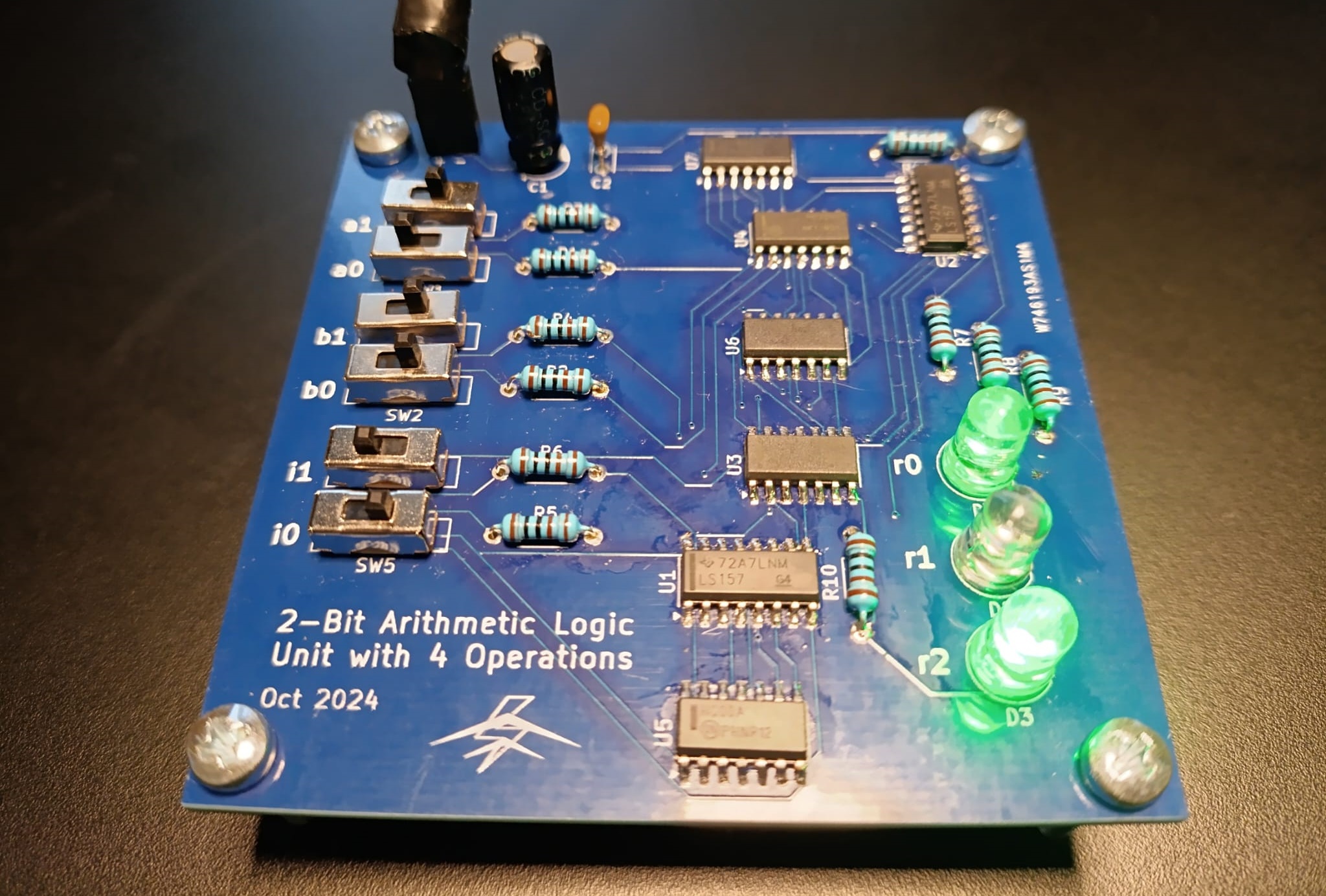
This 2-bit ALU (Arithmetic Logic Unit) is built using 74-series logic gates and multiplexers, and performs four basic operations: Logical AND, Logical OR, Addition, and positive-result Subtraction, on two 2-bit input words (A1A0 and B1B0). It uses a 2-bit opcode (I1I0) to select the operation, and displays the result as a 3-bit output (R2R1R0). Logical AND and OR operate only on the least significant bits (A0 and B0), with the result being displayed on R0. Arithmetic operations use the full words on input and output, and the output R2 is reserved for indicating overflow during addition.
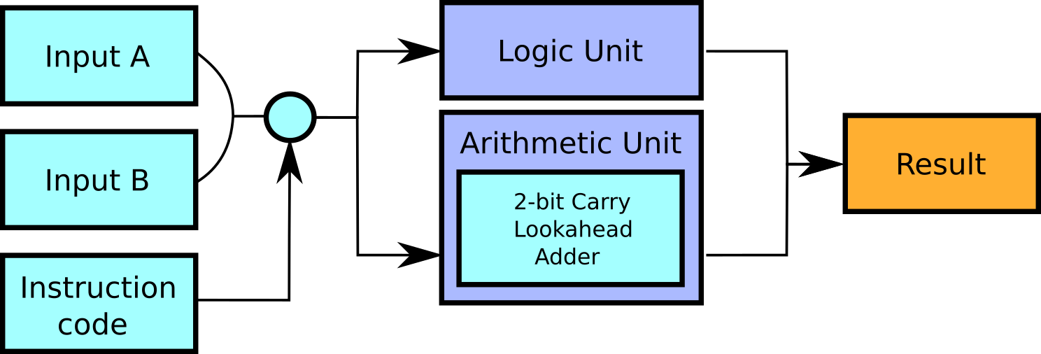
Logisim Evolution was used for the prototyping of the circuit and for simulating its functionality. (file provided in repository)
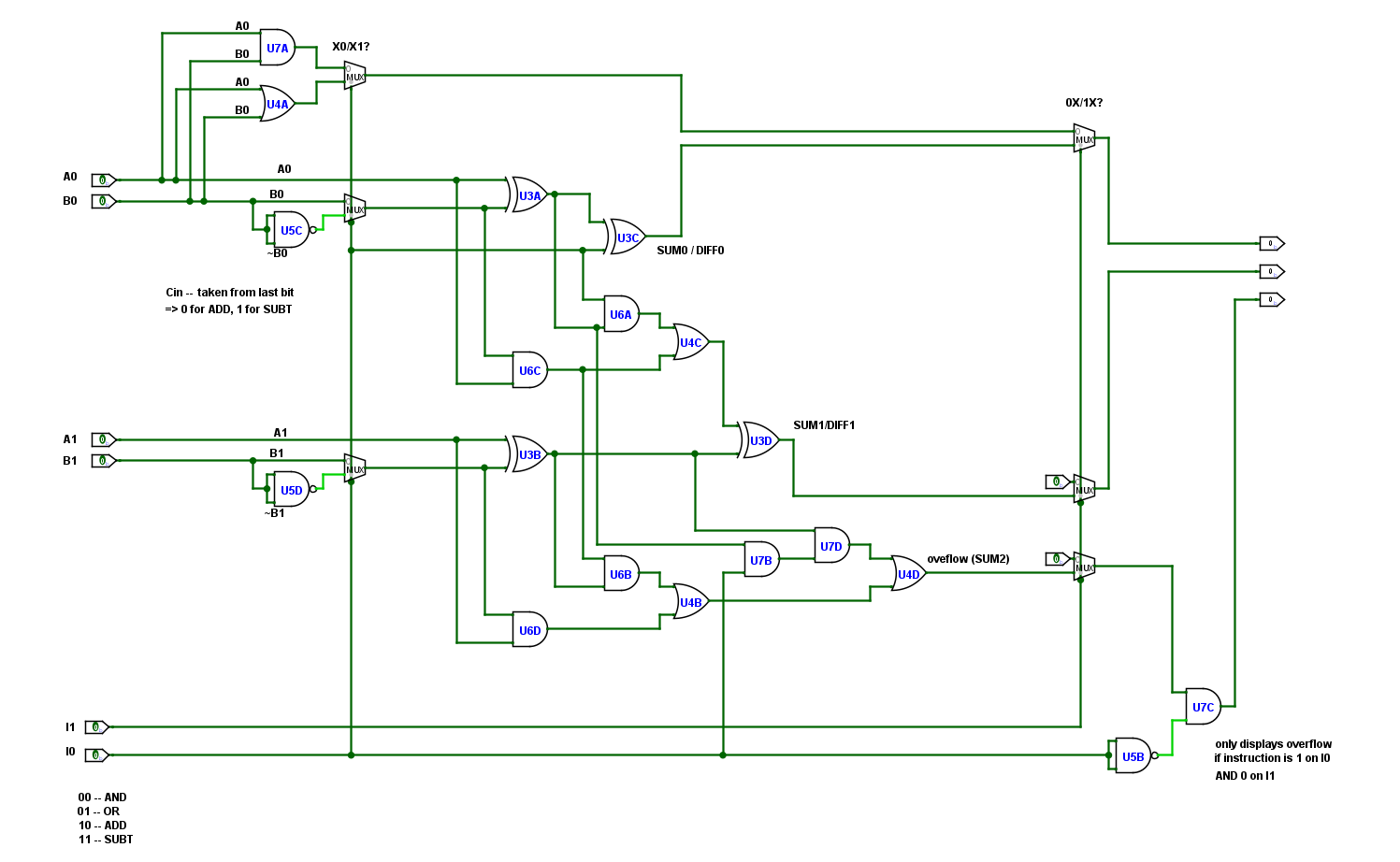
The project’s schematic and PCB were designed in KiCAD. (files provided in repository)
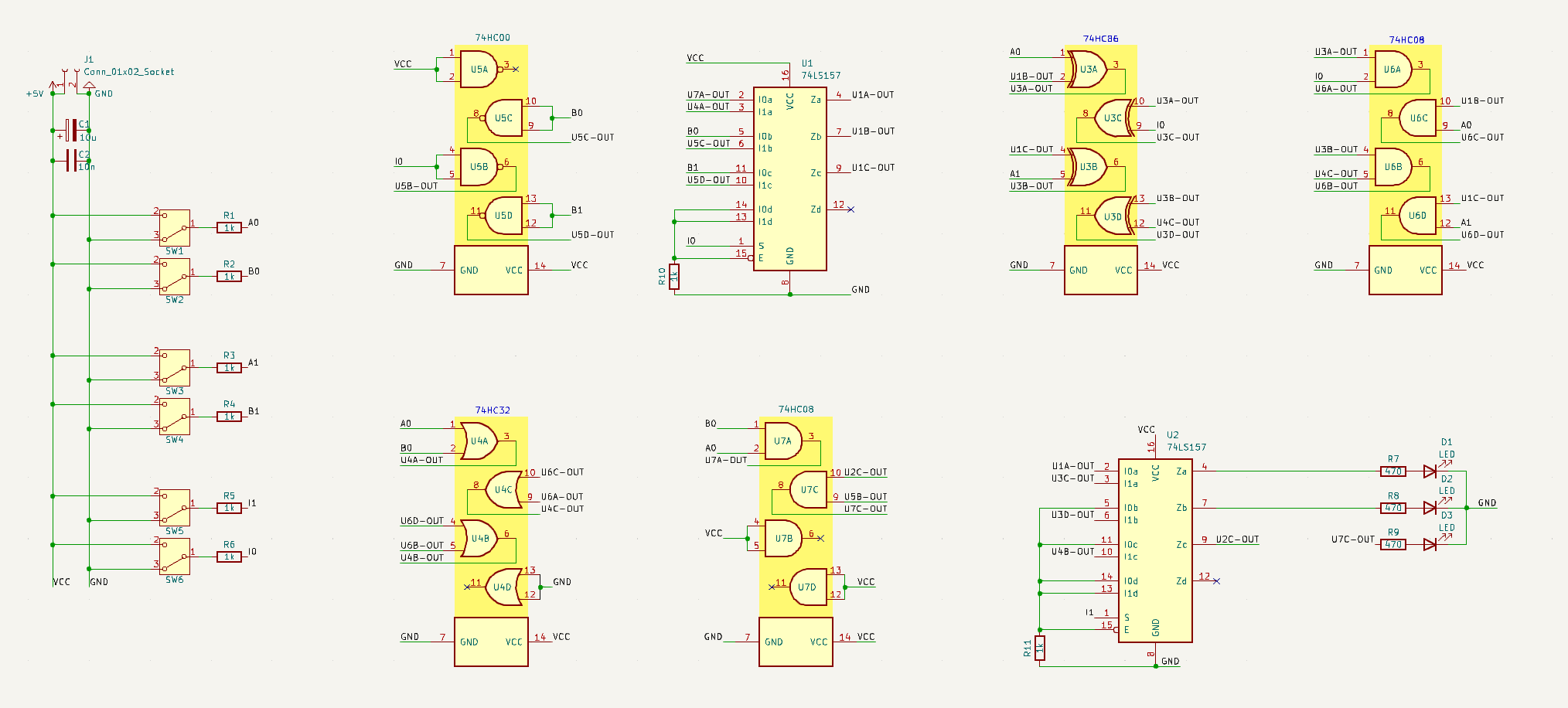
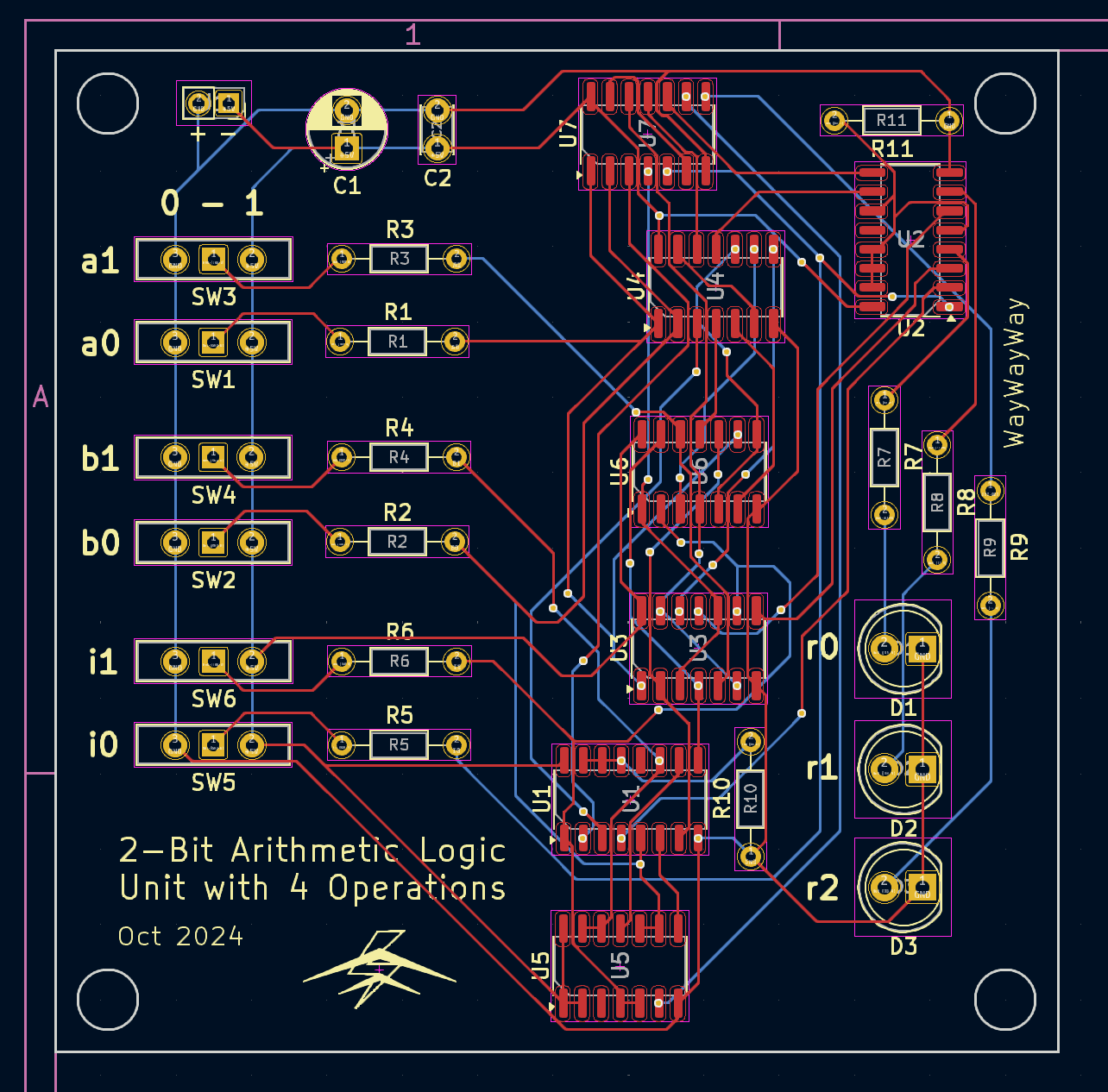
The ALU takes two 2-bit words (A1A0 and B1B0) as input for its operations, and one 2-bit word (I1I0) for selecting the opcode. The results of the operations are displayed using LEDs in the form of a 3-bit word (R2R1R0). The operations and their opcodes are as follows:
Logical AND 00
Logical OR 01
Addition 10
Subtraction 11
For the logical operations, only the least significant bits of the inputs - A0 and B0 - are operated upon, and the result is displayed on the result bit R0. The arithmetic operations employ the full 2-bit input word as well as two output bits, R1 and R0, while the third, R2, is reserved for displaying overflows from summations, and will remain LOW otherwise.
The general idea is that the input words A and B are forwarded to the operation-performing combinatorial logic gate circuits. Several multiplexers then select from among the results of the gate arrays, and based on the instruction opcode, the result of an operation is displayed. There are two arrays of multiplexers, corresponding to the 2-bit instruction word - I1 selects the arithmetic operations if 1, or the logic operations if 0. I0 further differentiates between the AND/OR, and SUM/DIFF operations.
The logic unit is quite simple, being composed of just an AND and an OR gate, handling the AND and OR operations, respectively. Both gates are active at the same time - the desired result is chosen using a 2-input multiplexer.
The arithmetic unit uses a 2-bit carry-lookahead adder (CLA for short) to perform addition and subtraction. The CLA adder works by taking 5 inputs - one for the carry-in of the summation of the LSB digits, as well as 4 more inputs consisting of the two 2-bit input words, A and B. The adder then outputs bits labeled to be the “sum” of each pair digits.
Generally, addition can be implemented with full adders, which work by taking as inputs two operators A, B, and a third input for the carry-in of the summation, and give as outputs one bit as the sum of the digits, and a second, which acts as the carry for a cascading summation. One full adder adds together one pair of digits, and many can be put in a cascading connection to produce a ripple-carry adder.
Initially, the design of this ALU employed, for its arithmetic unit, two full adders with ripple carry, rather than a CLA adder. Upon further analysis, however, it was determined that the two full adders, which operated without any synchronicity signal from a clock (the only way of avoiding timing issues with such a design), would have produced wrong results due to timing issues caused by propagation delays inherent in the logic gates. A pseudo-timing diagram follows:
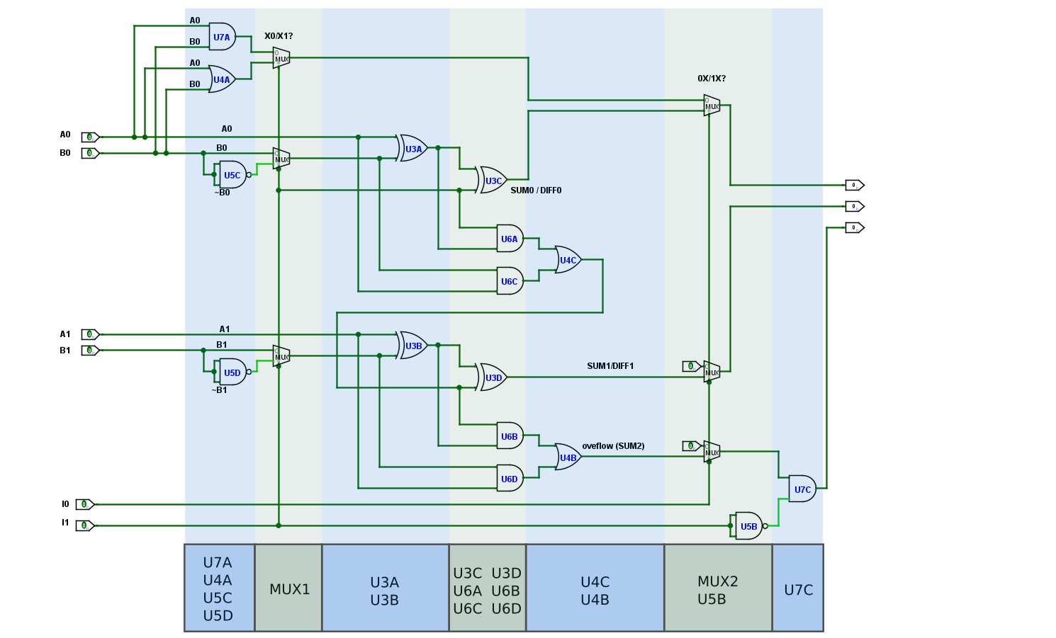 As can be seen from the schematic, the ripple-carry is sent from the first adder when the gate U4C fires its output, namely, in the 5th time period. This carry is meant to arrive at gate U3D – however, U3D fires in the 4th period, just before U4C, from which it is meant to receive its input. This is an obvious problem – U3D’s output will not account for the carry it was supposed to receive, since gate U4C had no time to send its output just yet.
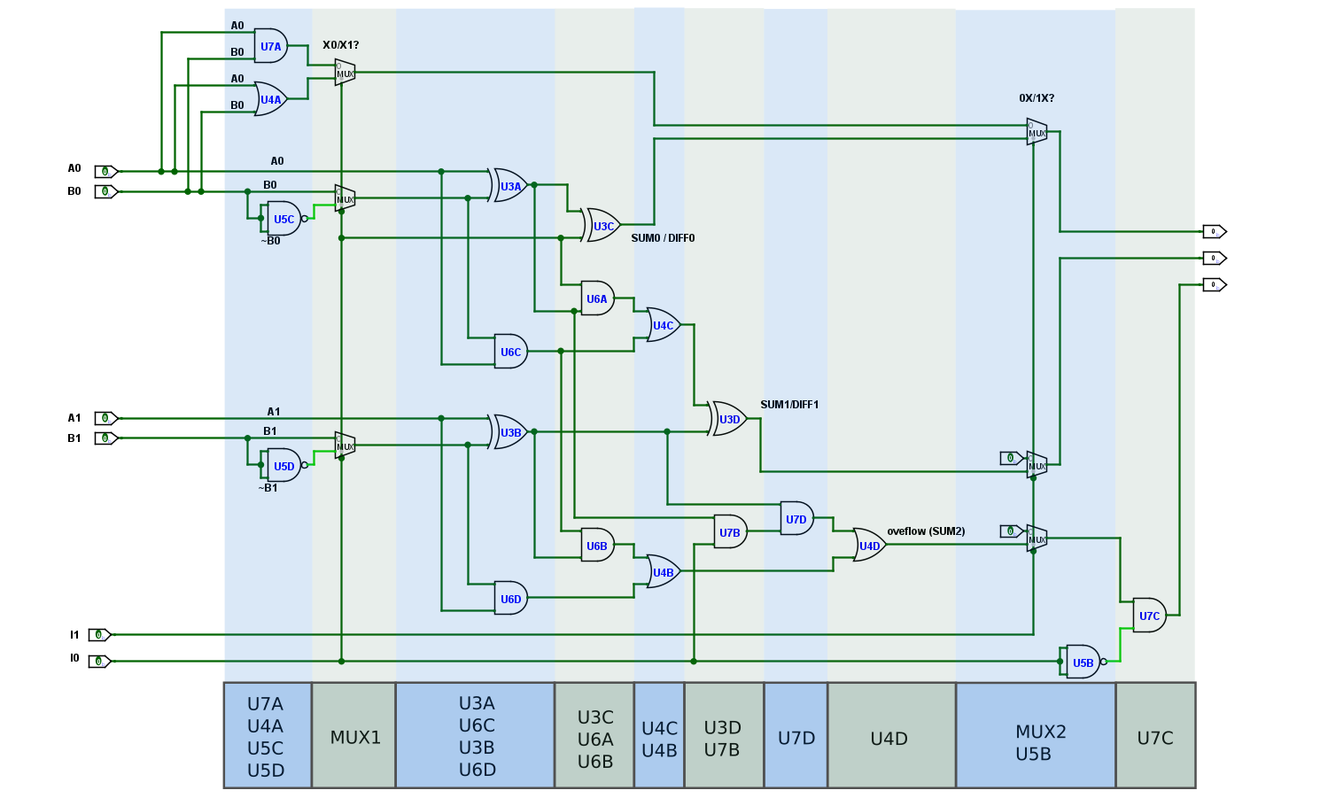 For a carry lookahead adder, however, no such issue exists – instead of waiting for the adders of less significant digits to finish their execution and send a ripple carry, the CLA adder uses extra logic circuitry that determines, based on the digits in the input words, whether a carry will be generated, before the adders dealing with said digits finish their execution. This absolves each individual adder of their dependency upon previous adder stages, allowing every individual pair to be summed up at the same time as, and without having to wait for, the others.
The design principle of the CLA adder is the avoidance of successive propagation, by predicting whether an operation will give a carry, before the operation occurs in the first place. This is done by introducing extra logic gates into the design, accounting for all possible situations that could result in a stage receiving a carry. Whether one of the adder stages in a CLA adder receives a carry depends on whether a previous stage has either generated a carry by itself, or propagated one from a stage before it. This ALU implements a 2-bit CLA adder, so the situations that it accounts for w.r.t. each carry are:
Carry-out 0:
Carry-out 1:
To further illustrate the principle, if we had to implement a 3-bit CLA adder, we would also have accounted for:
Carry-out 2:
... and so on, recursively, for any increase in width.
A further consideration regarding timing issues would be the propagation delays caused by the lengths of the PCB route traces – in high frequency circuits, the signals must arrive at the same time to their destinations. However, this ALU was implemented without clock timing in mind, and as such, the PCB route lengths do not matter, because given enough time, all signals will arrive, and the output will eventually be displayed correctly.
In the addition mode, the first adder stage is a simple full adder, which starts with a carry-in of zero and adds the digits as normal. The “sum” output is sent to the result LED output R0, while the carry is used with look-ahead in mind for the addition of the second pair of digits.
The second adder will similarly send the sum to the LED output on R1, but the process is slightly modified, and also, the carry-out of this stage will have accounted for the carry-out of the first adder, by checking all possible situations.
Since there is no third adder for the second carry-out to cascade to, any potential overflow will need to be displayed in order to produce the accurate result of the summation. The output R2 has been designated for this, and for all other situations, a circuit using two logic gates has been put in place to keep the state of R2 low.
Binary subtraction is performed using the two’s complement summation. This requires computing the two’s complement of the B input, which is done by inverting the digits of B and adding 1. For instance, for a B = 01, the two’s complement is obtained by inverting B, giving us “10”, and adding 1. Thus we have: 10 + 01 = 11.
The inversion of B can be done by applying inverters to each of B’s digits, this being implemented using NAND gates that are tied to B’s normal values. Seeing as addition and subtraction require the normal and the inverted values of B respectively, two multiplexers are used to select from among them, depending on the desired operation.
In the case of 2-bit operands, binary subtraction of A and the two’s complement of B therefore means:
A1 A0 +
B1’B0’+
0 1
With the normal inputs of A, as well as the inverted B which is selectable by the multiplexers, all that remains is providing an additional 1 to the summation. This can be conveniently done by passing the carry-in to the addition of A0 and B0 as 1 whenever subtraction is chosen as the operation; the carry-in would otherwise remain 0 when addition is performed. It so happens that the instruction bit I0 behaves exactly in this manner, allowing us to use it as the carry-in to the first adder stage.
It should be noted that the subtraction operation comes with some inherent caveats due to its employment of the two’s complement. For instance, without the logic gates that condition the output R2 solely to display the overflow of addition operations, the subtraction operation - itself employing summations, potentially overflowing - would also display overflows on the pin. The logic gates fix this, and the outputs on the other two LEDs are otherwise correct, if no overflow is displayed on R2.
Another functional incompleteness is found when performing subtractions that would give negative results. For instance, the operation 00 - 11 gives the result 100. Even without accounting for the output on R2, we can see how this is actually an integer overflow, arising as the result of 111 - 11. So, because we have no way of converting such overflows, nor otherwise handling signed integers, subtraction operations resulting in negative-signed results are completely unsupported by the circuit and will give an incorrect result.
SMD ICs:
Other components, THT:
| Qty | Value | Footprint | References |
|---|---|---|---|
| 8 | 1k | Resistor_THT:R_Axial_DIN0204_L3.6mm_D1.6mm_P7.62mm_Horizontal | R1, R2, R3, R4, R5, R6, R10, R11 |
| 6 | SW_Wuerth_450301014042 | Button_Switch_THT:SW_Slide-03_Wuerth-WS-SLTV_10x2.5x6.4_P2.54mm | SW1, SW2, SW3, SW4, SW5, SW6 |
| 3 | 470 | Resistor_THT:R_Axial_DIN0204_L3.6mm_D1.6mm_P7.62mm_Horizontal | R7, R8, R9 |
| 3 | LED | LED_THT:LED_D5.0mm_Clear | D1, D2, D3 |
| 2 | 74LS157 | Package_SO:SO-16_3.9x9.9mm_P1.27mm | U1, U2 |
| 1 | 10n | Capacitor_THT:C_Disc_D3.0mm_W2.0mm_P2.50mm | C2 |
| 1 | 10u | Capacitor_THT:CP_Radial_D5.0mm_P2.50mm | C1 |
| 1 | 74HC00 | Package_SO:SO-14_3.9x8.65mm_P1.27mm | U5 |
| 1 | 74HC08 | Package_SO:SO-14_3.9x8.65mm_P1.27mm | U7 |
| 1 | 74HC86 | Package_SO:SO-14_3.9x8.65mm_P1.27mm | U3 |
| 1 | 74LS08 | Package_SO:SO-14_3.9x8.65mm_P1.27mm | U6 |
| 1 | 74LS32 | Package_SO:SO-14_3.9x8.65mm_P1.27mm | U4 |
| 1 | Conn_01x02_Socket | Connector_PinSocket_2.00mm:PinSocket_1x02_P2.00mm_Vertical | J1 |
| 1 | LOGO | LOGO | G*** |
It measures 66.5 × 66.5 mm and has 2 copper layers, 1.6 mm thick.
31 parts, built around the 74LS157PC, 74HC00D, 74HC08D and 74HC86D. The full list of its parts is on this page, with links to each part's symbol and footprint where PCBKit's library has them.
From the constral/2-bit_alu repository on GitHub, at the commit this page was made from: the board is kicad project/2bit-ALU-90deg.kicad_pcb and its schematic kicad project/2bit-ALU.kicad_sch. PCBKit opens the board in the browser, with nothing to install.
Its repository states no licence, so its author keeps all rights: ask constral before reusing the design.
Trilobyte-CPU/8-bit-computer
A DIY 8-bit computer built mostly with discrete logic chips

slu4coder/Minimal-64x4-Home-Computer
My DIY TTL home computer with VGA and PS/2 and 4x the processing power of a Commodore C64 or Apple II.

slu4coder/Minimal-UART-Computer-1-2
Legacy: Version 1 and 2 of my TTL-only CPU featuring UART I/O, an expansion port, 512KB SSD at up to 10MHz clock speed

slu4coder/Minimal-64-Home-Computer
Legacy: Full TTL-only home computer with VGA and PS/2 and twice the processing power of a Commodore 64


Robert-Mones/Claculator
A reverse Polish notation calculator with added features such as comparisons, branching, and custom recursive operators taken from the Clac project from the 15-122 course at Carnegie Mellon University.

nailed-barnacle/Cisc-8-ttl-processor
A cut-down version of the 8080 processor using HCTTL and including a discrete ALU and instruction decoder
