
2 layers243.2 × 106 mm

 cjsilman/atmega-breakout-PCB3
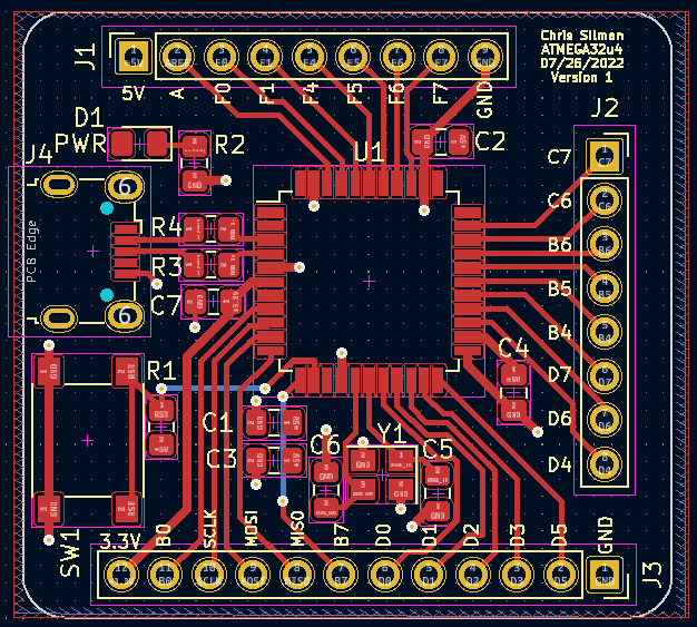
This PCB project is meant to replicate a simple atmega32u4 microcontroller board with GPIO pinouts. It contains a peripheral USB for programming and powering
Arduino Clone is an open-source printed circuit board by cjsilman, from the cjsilman/atmega-breakout-PCB repository on GitHub, published under the GPL-3.0 licence. It is a 2-layer board of 37.5 × 35 mm with 19 parts on 39 nets, routed with 163 tracks and 20 vias.
It is built around the ATMEGA32U4-AU. Its parts include 7 capacitors, 4 resistors, 4 connectors, 1 IC and 1 diode. It belongs with the AVR (ATmega, ATtiny) boards of this library.
This PCB project is meant to replicate a simple atmega32u4 microcontroller board with GPIO pinouts. It contains a USB port for programming and powering.
As the idea of designing my own PCB always fascinated me, I thought it would be interesting to give designing one a shot!
While searching around the market for which MCU to use, I choose the ATMEGA32u4 as it comes with a pre-installed bootloader, allowing you to program it via the USB right from the start. This MCU also came with USB support, something I wanted in my PCB. It was quite the learning process. I feel like I learned quite a bit that I want to share.
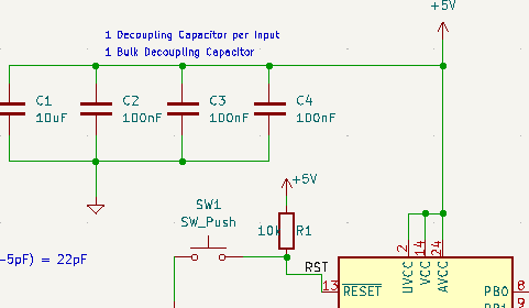
To begin with, you typically start by setting up the main components the MCU needs to function: it's power and crystal oscillator.
When designing the schematic for the VCC pins, it is best practice to place a 100nF decoupling capacitor for each pin along with a 10uF bulk decoupling capcitor to help with the stabilization of the input voltage.
For the crystal oscillator, you'll want to calculate the value of the decoupling capacitors associated with it. While it is standard practice to use 22pF capacitors, it is important to choose proper capacitor values to allow for more accurate and stable results from the crystal.
The capacitor values can be calculated from a formula like this:
Cload, or the load capacitance, is retrieved from the datasheet of the specific crystal you choose.
Cstray, or the stray capacitance, is typically between a value of 3-5pF.

If you ever find yourself lost, the MCU datasheet typically has a lot of guidelines for when it comes to designing with that specific IC. Make sure to follow them.
I placed a GND plane on the entire bottom layer of my PCB. This allows for better signal integrity and more resistance to interference, it also allows you to create a via to ground wherever you need it.
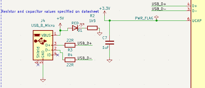
I discovered that USBs are typically designed with something known as "differential pairs"
If you have any advice for me or would like to talk to me about certain design decisions feel free to give me a message! I am always looking to learn new things and improve my knowledge

| Qty | Value | Footprint | References |
|---|---|---|---|
| 3 | 100nF | Capacitor_SMD:C_0805_2012Metric_Pad1.18x1.45mm_HandSolder | C2, C3, C4 |
| 2 | 22R | Resistor_SMD:R_0805_2012Metric_Pad1.20x1.40mm_HandSolder | R3, R4 |
| 2 | 22pF | Capacitor_SMD:C_0805_2012Metric_Pad1.18x1.45mm_HandSolder | C5, C6 |
| 1 | 10k | Resistor_SMD:R_0805_2012Metric_Pad1.20x1.40mm_HandSolder | R1 |
| 1 | 10uF | Capacitor_SMD:C_0805_2012Metric_Pad1.18x1.45mm_HandSolder | C1 |
| 1 | 16MHz | Crystal:Crystal_SMD_3225-4Pin_3.2x2.5mm | Y1 |
| 1 | 1k5 | Resistor_SMD:R_0805_2012Metric_Pad1.20x1.40mm_HandSolder | R2 |
| 1 | 1uF | Capacitor_SMD:C_0805_2012Metric_Pad1.18x1.45mm_HandSolder | C7 |
| 1 | ATmega32U4-A | Package_QFP:TQFP-44_10x10mm_P0.8mm | U1 |
| 1 | Conn_01x08_Female | Connector_PinSocket_2.54mm:PinSocket_1x08_P2.54mm_Vertical | J2 |
| 1 | Conn_01x09_Female | Connector_PinSocket_2.54mm:PinSocket_1x09_P2.54mm_Vertical | J1 |
| 1 | Conn_01x12_Female | Connector_PinSocket_2.54mm:PinSocket_1x12_P2.54mm_Vertical | J3 |
| 1 | RED | LED_SMD:LED_0805_2012Metric_Pad1.15x1.40mm_HandSolder | D1 |
| 1 | SW_Push | Button_Switch_SMD:SW_Push_1P1T_NO_6x6mm_H9.5mm | SW1 |
| 1 | USB_B_Micro | Connector_USB:USB_Micro-B_Wuerth_629105150521 | J4 |

tominabox1/Le-Chiffre-Keyboard
Great thanks goes to Jake at P3D for really making the case amazing and open sourcing his work. Check him out at P3Dstore.com

The-Royal/The_Royal_Open-Source-Projects
A Master Repository For All things Royal Made

dpapavas/lagrange-keyboard
A configurable, handwired, ergonomic keyboard

dmcke5/ZenDeck
This is the second revision of my Mini PC based handheld Gaming PC! It is designed for a Beelink SER 5 Mini PC but could be adapted to other systems by changing the mounting brackets and outlet plate.


thebiguno/microcontroller-projects
A home for a bunch of microcontroller projects which don't warrant their own repos.

swiftrax/UnSplit
Ergo 40% mechanical keyboard with all components on the top with diodes arranged in an array
It measures 37.5 × 35 mm and has 2 copper layers, 1.6 mm thick.
19 parts, built around the ATMEGA32U4-AU. The full list of its parts is on this page, with links to each part's symbol and footprint where PCBKit's library has them.
From the cjsilman/atmega-breakout-PCB repository on GitHub, at the commit this page was made from: the board is Arduino_Clone.kicad_pcb and its schematic Arduino_Clone.kicad_sch. PCBKit opens the board in the browser, with nothing to install.
Its repository publishes it under the GPL-3.0 licence: you may reuse it on that licence's terms (keep the author's notice, and for a copyleft licence share your changes alike).