4 layers70.4 × 107.2 mm
 cjheath/jlcbasic5
JLC Basic parts library for Kicad fetched and converted from EasyEDA
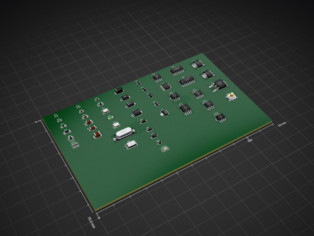
Jlctest is an open-source printed circuit board by cjheath, from the cjheath/jlcbasic repository on GitHub. It is a 2-layer board of 121 × 75.5 mm with 46 parts on 177 nets.
It is built around the SP485EEN-L, LM324DT and NE5532DR-MS, with the OP07CDRG, TL072CDT and TPS5430DDAR among its other parts. Its parts include 12 ICs, 9 diodes, 6 capacitors, 5 resistors and 5 transistors.


| Qty | Value | Footprint | References |
|---|---|---|---|
| 1 | 0Ω | jlcbasic:R1206 | R4 |
| 1 | 0Ω | jlcbasic:R0603 | R2 |
| 1 | 0Ω | jlcbasic:R0805 | R3 |
| 1 | 0Ω | jlcbasic:R0402 | R1 |
| 1 | 100uF | jlcbasic:CASE-B_3528 | C6 |
| 1 | 100Ω@100MHz | jlcbasic:L0805 | L2 |
| 1 | 10nF | jlcbasic:C0603 | C2 |
| 1 | 10uF | jlcbasic:CAP-SMD_L3.2-W1.6-RD-C7171 | C5 |
| 1 | 10Ω | jlcbasic:R0805_NEW | R5 |
| 1 | 12MHz | jlcbasic:CRYSTAL-SMD_4P-L3.2-W2.5-BL | X3 |
| 1 | 16MHz | jlcbasic:OSC-SMD_4P-L3.2-W2.5-BL | X1 |
| 1 | 1KΩ | jlcbasic:RES-ARRAY-SMD_0603-8P-L3.2-W1.6-BL | RN1 |
| 1 | 1N4148ST4 | jlcbasic:SOD-323_L1.8-W1.3-LS2.5-RD | D8 |
| 1 | 1N4148W | jlcbasic:SOD-123F_L2.7-W1.6-LS3.8-RD | D5 |
| 1 | 1nF | jlcbasic:C0402 | C1 |
| 1 | 1nF | jlcbasic:C1206 | C4 |
| 1 | 32.768kHz | jlcbasic:FC-135R_L3.2-W1.5 | X2 |
| 1 | 33nF | jlcbasic:C0805 | C3 |
| 1 | 600Ω@100MHz | jlcbasic:L0603 | L1 |
| 1 | 74HC595 | jlcbasic:SOIC-16_L9.9-W3.9-P1.27-LS6.0-BL | U6 |
| 1 | 8MHz | jlcbasic:CRYSTAL-SMD_L11.5-W4.8-LS12.7 | X4 |
| 1 | 8MHz | jlcbasic:CRYSTAL-SMD_L5.0-W3.2 | X5 |
| 1 | AMS1117-3.3 | jlcbasic:SOT-223-3_L6.5-W3.4-P2.30-LS7.0-BR | U8 |
| 1 | AMS1117-5.0 | jlcbasic:SOT-223_L6.5-W3.5-P2.30-LS7.0-BR | U9 |
| 1 | AO3401A | jlcbasic:SOT-23_L2.9-W1.3-P1.90-LS2.4-BR | Q4 |
| 1 | B5819W | jlcbasic:SOD-123_L2.7-W1.6-LS3.7-RD-1 | D7 |
| 1 | D882 | jlcbasic:SOT-89-3_L4.5-W2.5-P1.50-LS4.2-BR | Q5 |
| 1 | L78M05 | jlcbasic:TO-252-2_L6.5-W6.1-P4.58-LS10.0-TL | U10 |
| 1 | LM324DT | jlcbasic:SOIC-14_L8.7-W3.9-P1.27-LS6.0-BL | U5 |
| 1 | MMBT5551 | jlcbasic:SOT-23-3_L2.9-W1.3-P1.90-LS2.4-BR | Q1 |
| 1 | NE5532DR | jlcbasic:SOIC-8_L4.9-W3.9-P1.27-LS6.0-BL | U11 |
| 1 | OP07CDR | jlcbasic:SOIC-8_L4.9-W3.9-P1.27-LS6.0-BL | U1 |
| 1 | P6SMB6.8CA | jlcbasic:SMB_L4.6-W3.6-LS5.3-BI | D4 |
| 1 | S8550 | jlcbasic:SOT-23-3_L2.9-W1.6-P1.90-LS2.8-BR | Q2 |
| 1 | SI2301CDS | jlcbasic:SOT-23-3_L3.0-W1.7-P0.95-LS2.9-BR | Q3 |
| 1 | SM4007PL | jlcbasic:SOD-123F_L2.8-W1.8-LS3.7-RD | D6 |
| 1 | SP3232EEY | jlcbasic:TSSOP-16_L5.0-W4.4-P0.65-LS6.4-BL | U7 |
| 1 | SP485EEN | jlcbasic:SOIC-8_L5.0-W4.0-P1.27-LS6.0-BL | U3 |
| 1 | SS34 | jlcbasic:SMA_L4.3-W2.6-LS5.2-RD | D1 |
| 1 | SS54 | jlcbasic:SMA_L4.4-W2.8-LS5.4-R-RD | D2 |
| 1 | TL072CDT | jlcbasic:SOIC-8_L5.0-W4.0-P1.27-LS6.0-BL | U12 |
| 1 | TPS5430DDAR | jlcbasic:ESOP-8_L4.9-W3.9-P1.27-LS6.0-TL-EP | U2 |
| 1 | TS-1187A-B-A-B | jlcbasic:SW-SMD_4P-L5.1-W5.1-P3.70-LS6.5-TL_H1.5 | SW1 |
| 1 | US1MG | jlcbasic:SMA_L4.4-W2.8-LS5.4-RD | D3 |
| 1 | W25Q128JVSIQTR | jlcbasic:SOIC-8_L5.3-W5.3-P1.27-LS8.0-BL | U4 |
| 1 | whiteLEDSMD | jlcbasic:LED0805-R-RD | LED1 |
It measures 121 × 75.5 mm and has 2 copper layers, 1.6 mm thick.
46 parts, built around the SP485EEN-L, LM324DT, NE5532DR-MS and OP07CDRG. The full list of its parts is on this page, with links to each part's symbol and footprint where PCBKit's library has them.
From the cjheath/jlcbasic repository on GitHub, at the commit this page was made from: the board is jlctest/jlctest.kicad_pcb and its schematic jlctest/jlctest.kicad_sch. PCBKit opens the board in the browser, with nothing to install.
Its repository states no licence, so its author keeps all rights: ask cjheath before reusing the design.


Serhio4522/SEM_hitachi-
Digitization of a Hitachi scanning electron microscope (SEM) — hardware design, FPGA firmware, and analog frontend schematics.


profdc9/RFUtilityKnifeBFP740
The RF Utility Knife PCB, redone for the BFP740 44 GHz transistor

photon-cat/envcontrol
tools better environmental controller for poultry, switchboard and relay hardware

