
2 layers98 × 135 mm
 ciwhitfill/buffer-pedal11
Design and documentation for guitar buffer pedal
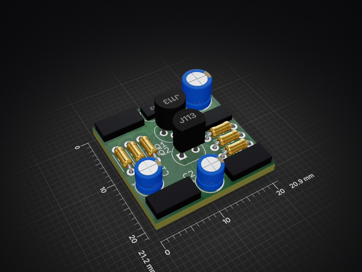
Buffer pedal is an open-source printed circuit board by ciwhitfill, from the ciwhitfill/buffer-pedal repository on GitHub. It is a 2-layer board of 20.9 × 21.2 mm with 17 parts on 8 nets, routed with 31 tracks and 0 vias.
It is built around the J113. Its parts include 6 resistors, 3 capacitors, 2 diodes and 2 transistors. It belongs with the audio and music boards of this library.
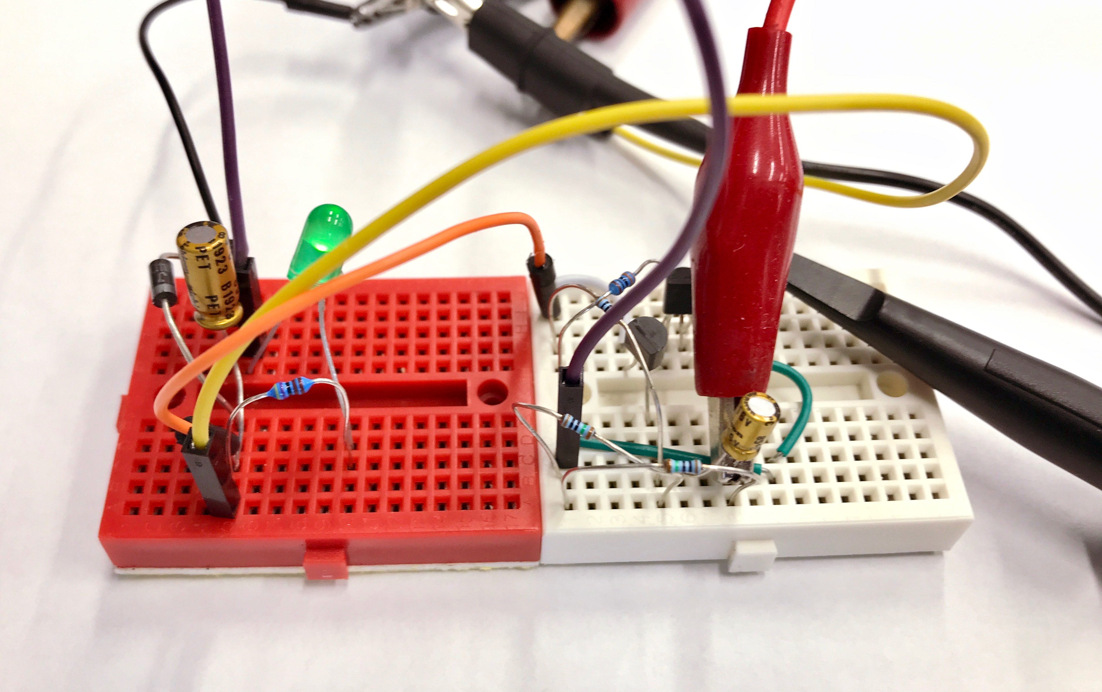
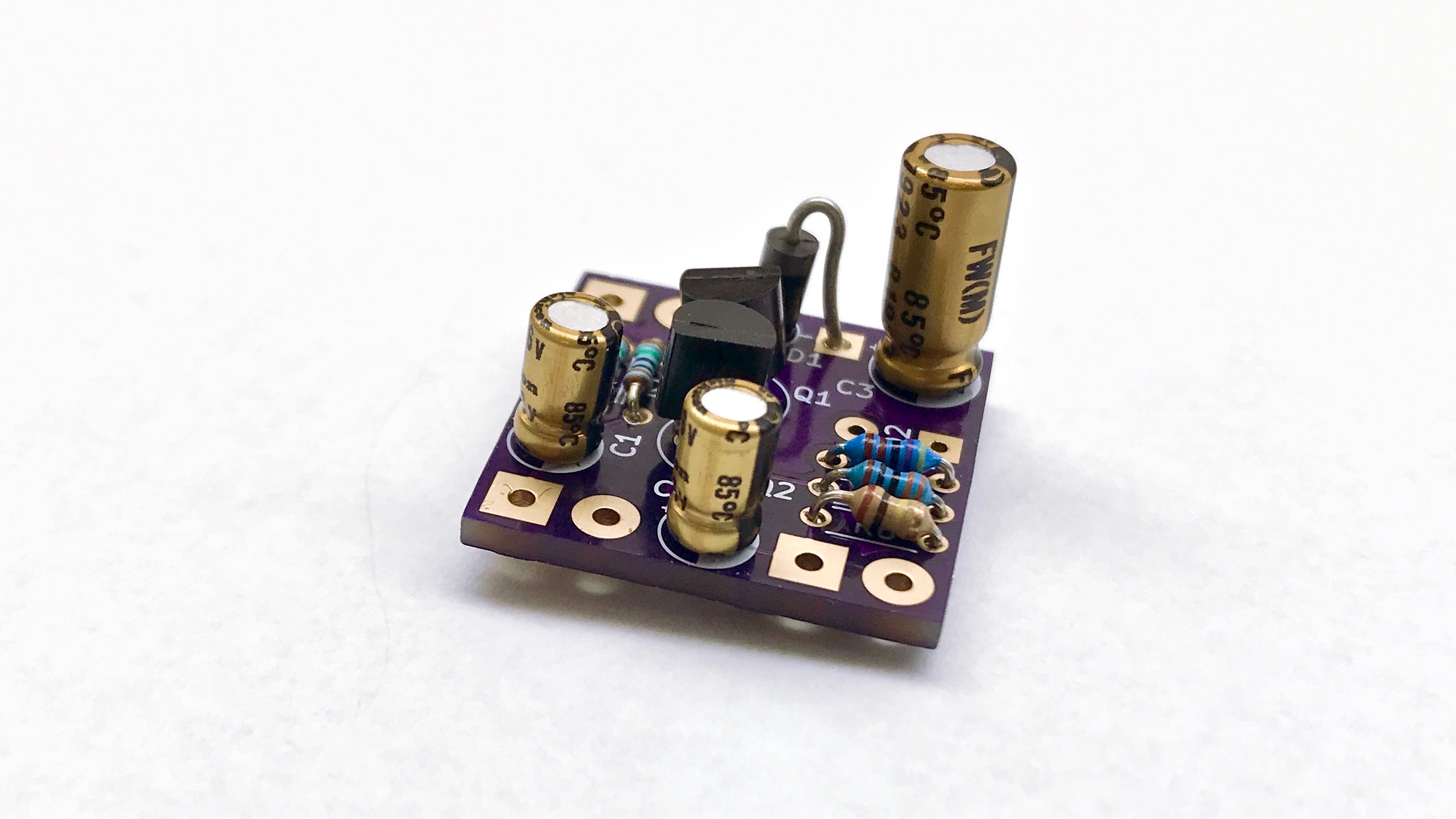
This project documents the design and construction of a JFET buffer guitar pedal.
| Quantity | Designators | Description | Value | Package | Mouser Part # |
|---|---|---|---|---|---|
| 3 | R1, R2, R3 | Resistor | 10Mohm, 1/8W | 3.6mm | 594-5063JD10M00FT |
| 1 | R 5 | Resistor | 330ohms, 1/8W | 3.6mm | 603-MFR-12FTF52-330R |
| 1 | R6 | Resistor | 100Kohms, 1/8W | 3.6mm | 603-CFR-12JT-52-100K |
| 1 | R7 | Resistor | 4.7Kohms, 1/8W | 3.6mm | 603-MFR-12FTF52-4K7 |
| 2 | C1, C2 | Capacitor, polarized | 10uF, 16V | 4mm | 647-USW1C100MDD |
| 1 | C3 | Capacitor, polarized | 47uF, 25V | 5mm | 647-UFW1E470MDD |
| 2 | Q1, Q2 | N-Channel JFET | J113 | TO-92 | 512-J113 |
| 1 | D1 | Diode | 1N4003 | DO-41 | 583-1N4003-T |
| 1 | D2 | LED | Green | 5mm | 859-LTL2R3KGD-EM |
| 2 | J1, J2 | Phone Connector | 1/4" TS | 568-NYS229 | |
| 1 | J3 | DC Power Connector | 2.1mm | 163-1060-EX |
The circuit consists of a JFET source follower with an active load. Compared to passive biasing, an active load provides an operating point that is stable over a much larger range of voltages. This allows the amplifier to drive lower impedance loads at lower supply voltages.
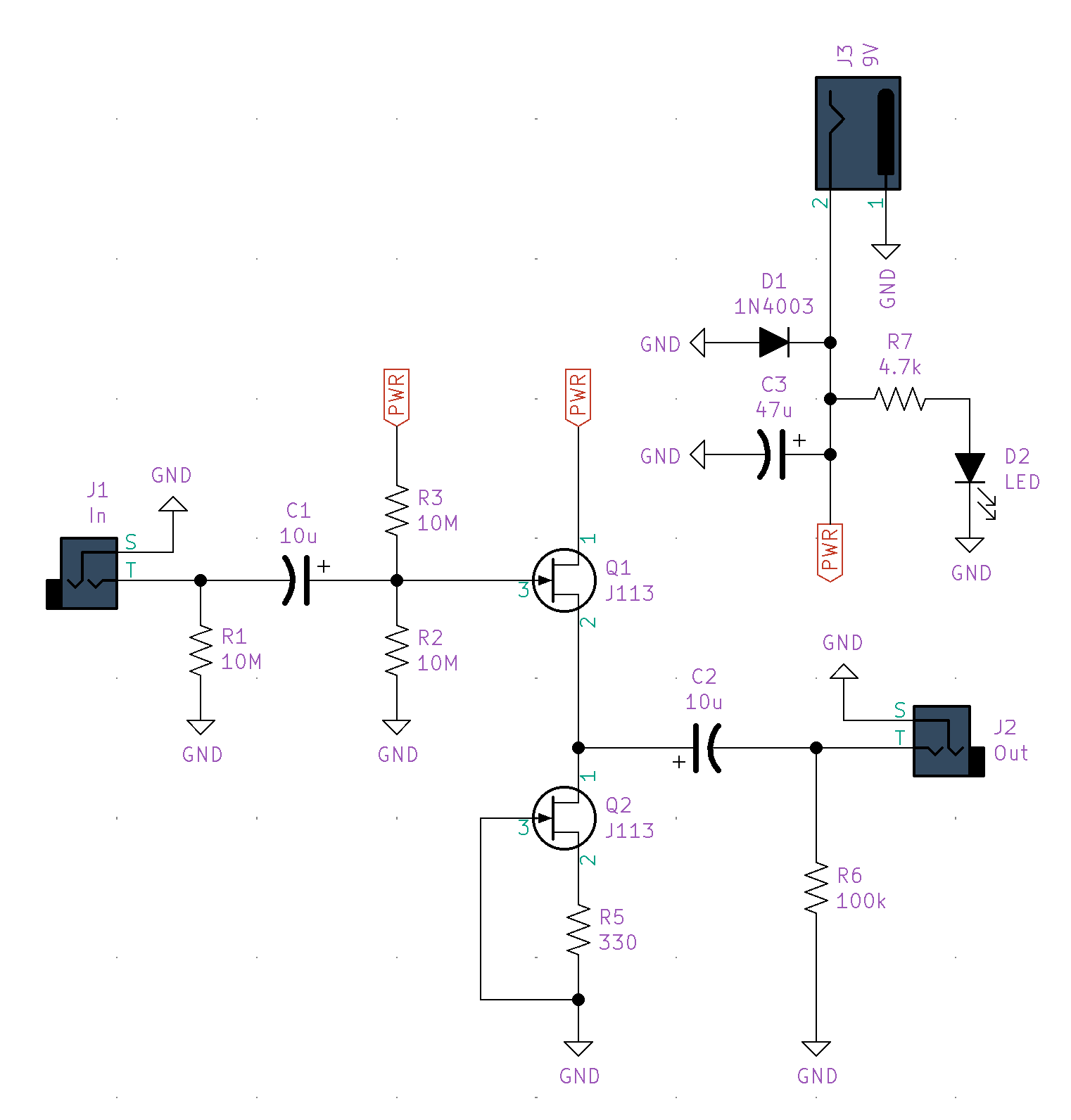
The following simulations were conducted in LTspice. For the schematic file and simulation results, see the simulation folder.
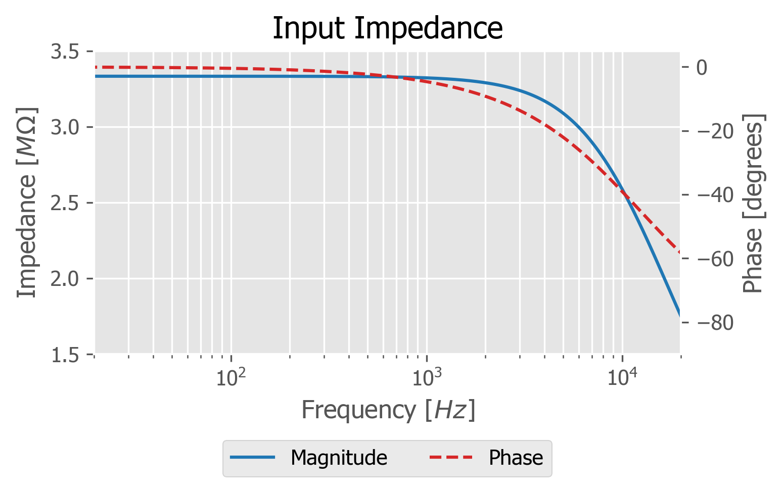
A high input impedance is necessary to avoid loading passive guitar pickups. Generally, an input impedance of at least 1 MΩ is desired. The design provides this impedance throughout the audio range.
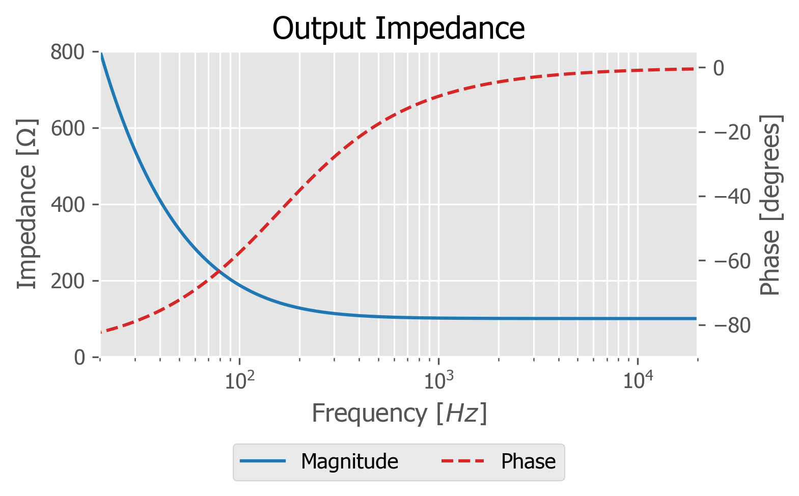
The design provides a low enough output impedance to drive line-level inputs. While the coupling capacitor dominates at low frequencies, the output impedance asymptotes to 100 Ω, which is more than sufficient for instrument level applications.
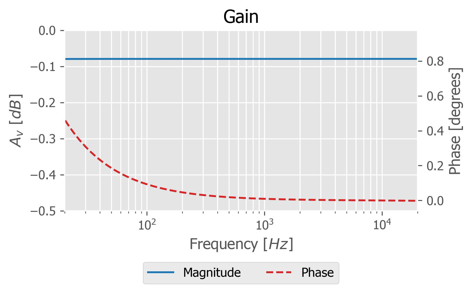
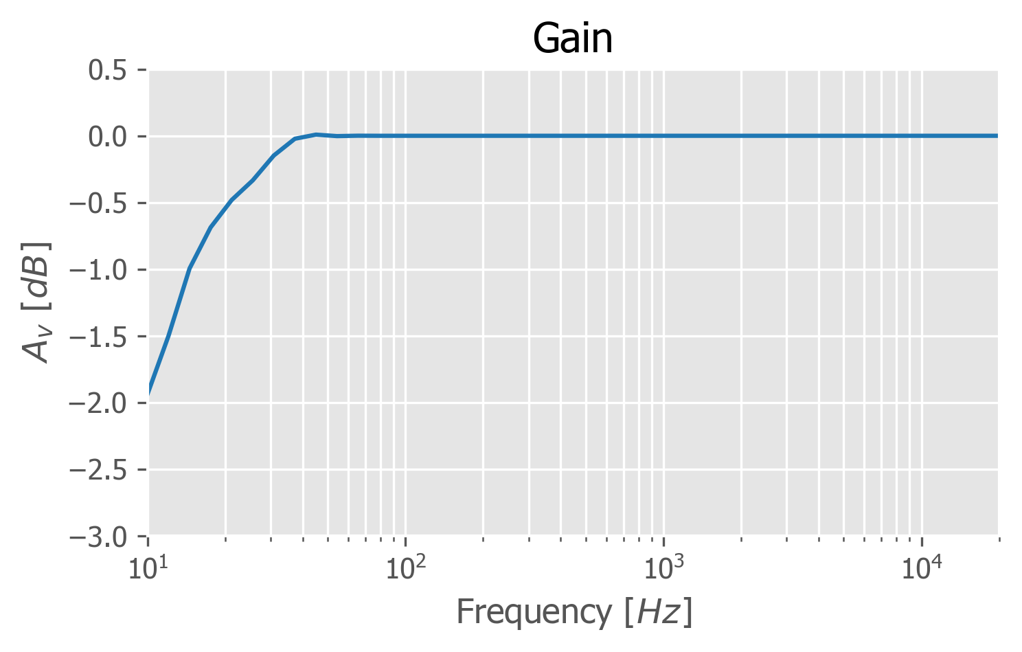
A good voltage buffer has as close to a gain of 1 as possible. Due to the higher impedance of the active load, the design comes within 0.1 dB of this.
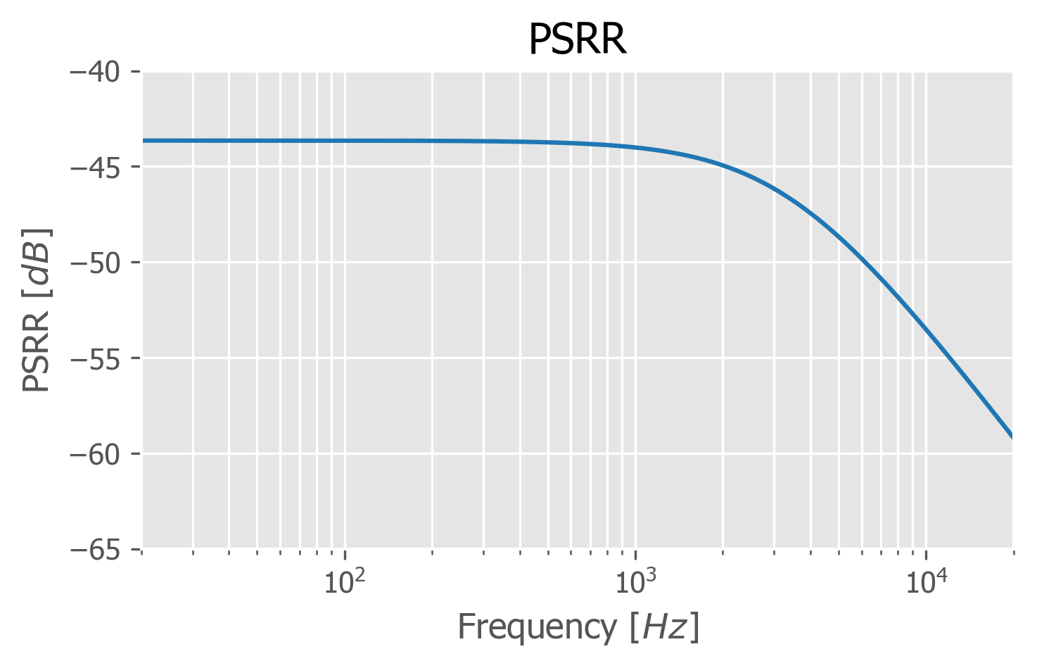
The design has a PSRR of -43dB at DC, and the power supply capacitor further filters supply noise at high frequencies.
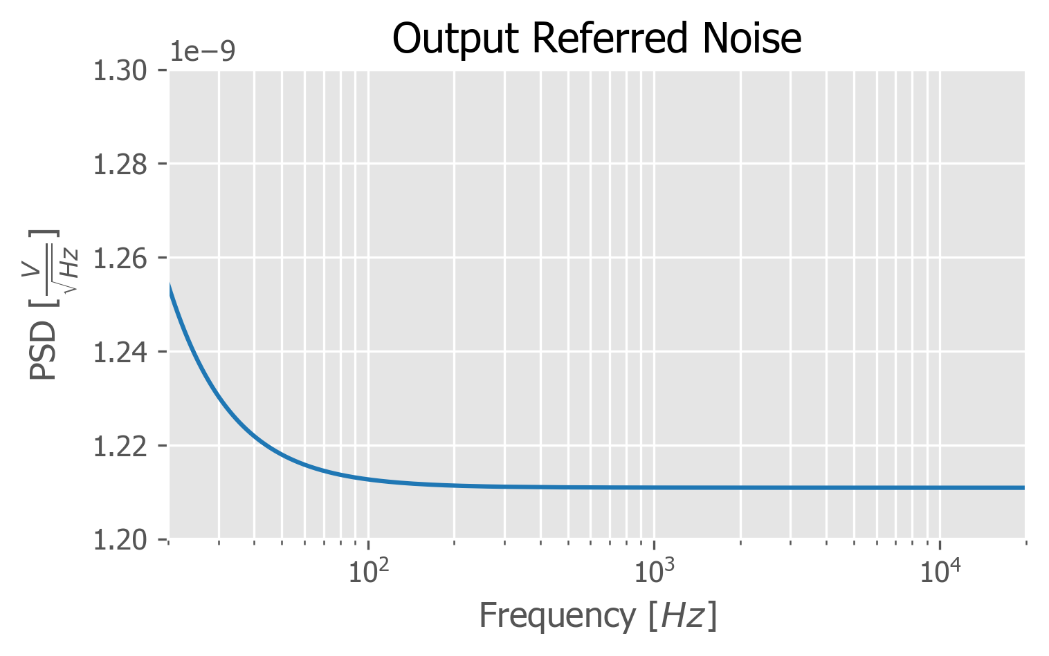
Noise simulation results in 171.18 nV in the audio range. Even if actual circuit noise is many times worse, it will be negligible compared to other noise sources in the signal chain.
When a 1 V, 1 kHz test signal is applied to the input, the buffer reproduces it at the output within the precision of the test equipment available.
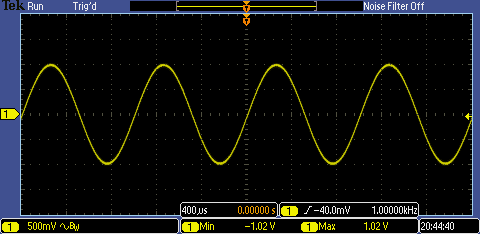
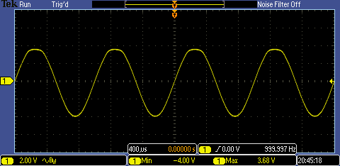
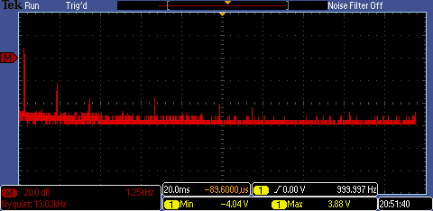
When overdriven, the buffer clips asymmetically, resulting in predominantly 2nd-order harmonic distortion. In guitar circuits, this is generally preferred to the odd-order distortion of amplifiers with high loop gain.
In practice, the amplifier exhibits mild roll-off of sub-bass frequencies below 30 Hz. This is well below the necessary bandwidth of a guitar amplifier. The high-end frequency response extends well above the audio band, ensuring accurate phase response.
| Qty | Value | Footprint | References |
|---|---|---|---|
| 3 | 10M | Resistor_THT:R_Axial_DIN0204_L3.6mm_D1.6mm_P5.08mm_Horizontal | R1, R2, R3 |
| 2 | 10u | Capacitor_THT:CP_Radial_D4.0mm_P1.50mm | C1, C2 |
| 2 | J113 | Package_TO_SOT_THT:TO-92 | Q1, Q2 |
| 1 | 100k | Resistor_THT:R_Axial_DIN0204_L3.6mm_D1.6mm_P5.08mm_Horizontal | R6 |
| 1 | 1N4003 | Diode_THT:D_DO-41_SOD81_P3.81mm_Vertical_KathodeUp | D1 |
| 1 | 330 | Resistor_THT:R_Axial_DIN0204_L3.6mm_D1.6mm_P5.08mm_Horizontal | R5 |
| 1 | 4.7k | Resistor_THT:R_Axial_DIN0204_L3.6mm_D1.6mm_P5.08mm_Horizontal | R7 |
| 1 | 47u | Capacitor_THT:CP_Radial_D5.0mm_P2.00mm | C3 |
| 1 | 9V | Connector_Wire:SolderWirePad_1x02_P3.81mm_Drill1.2mm | PWR |
| 1 | In | Connector_Wire:SolderWirePad_1x02_P3.81mm_Drill1.2mm | IN |
| 1 | LED | Connector_Wire:SolderWirePad_1x02_P3.81mm_Drill1mm | D2 |
| 1 | LOGO | tst:Bluet | G*** |
| 1 | Out | Connector_Wire:SolderWirePad_1x02_P3.81mm_Drill1.2mm | OUT |
It measures 20.9 × 21.2 mm and has 2 copper layers, 1.6 mm thick.
17 parts, built around the J113. The full list of its parts is on this page, with links to each part's symbol and footprint where PCBKit's library has them.
From the ciwhitfill/buffer-pedal repository on GitHub, at the commit this page was made from: the board is Buffer_Pedal.kicad_pcb. PCBKit opens the board in the browser, with nothing to install.
Its repository states no licence, so its author keeps all rights: ask ciwhitfill before reusing the design.


mprosk/wow_and_flutter
Wow & Flutter is a pitch modulation source, that generates triangle and sample and hold with slew

DeMarco/DMH-S-H-Noise
Implementation of the S&H + Noise Generator circuits by Moritz Klein into Kosmo format.

grahamseamans/pi-psu
A 5V linear power supply designed for Raspberry Pi and similar devices.

OscarBazylewich/Phaser_and_Overdrive_Custom_Guitar_Pedal
This project is a guitar pedal with analog circuits. It has a four-stage JFET phaser of the MXR Phase 90 type and a diode-clipping overdrive of the BOSS OD-1 type.