
2 layers100 × 100 mm
Pico dram tester
schlae/pico-dram-tester
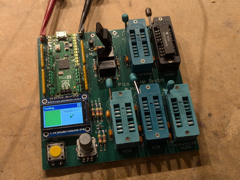
Raspberry Pi Pico 2 Vintage DRAM Tester
47 parts165CC-BY-SA-4.0

 ChrisWeiss/RAMTester
Open source hardware tester for GM71C16100AJ6 chips
Pico dram tester is an open-source printed circuit board by ChrisWeiss, from the ChrisWeiss/RAMTester repository on GitHub. It is a 2-layer board of 100 × 100 mm with 44 parts on 64 nets, routed with 825 tracks and 218 vias.
It is built around the RFM-0505S. Its parts include 10 capacitors, 10 resistors, 9 ICs, 2 connectors and 2 switches. It belongs with the RP2040 and RP2350 boards of this library.
Having trouble with your old-school DIP dynamic RAM chips? Here's a simple RAM tester that will give you a definitive pass or fail for a variety of chips.
This is an early beta release. The software is not completed. Feel free to build a tester and try it out, and submit bug reports.
Benefits
Supported Devices
Out of scope
The board is a simple 2-layer board, 100mm x 100mm, and 1.6mm thick. Fabricate at your favorite vendor in any color you wish.
You may populate the board only with the sockets for devices you plan to use, or you may populate all the sockets. You can try substituting the sockets with standard IC sockets, but I recommend ZIF sockets which are much easier to use. Why so many sockets? It saves you from having to install dozens of pin control transistors required to make a tester work with a single universal socket.
Populate Q1, U7, U8, R2, R3, R4, and R5 if you would like to test 4116 and 4132 devices without requiring an external -5V and +12V power supply.
If you want to provide the -5V, +5V, and +12V power from your bench supply, then you may leave those components off of the board and connect your power leads to the -5V, +5V, and +12V test points. If you don't plan to test 4116 or 4132 chips, then you can safely leave out those components.
The LCD display is nominally the Adafruit 4383 which is to be installed at location J1 (U9 is not required when using this display). You can also use cheaper devices available from Aliexpress and others. They are 8-pin LCD displays sold as 1.14" 135x240 IPS ST7789 modules. Install this display at position J2. You may also need to add the voltage monitor at position U9.
For several reasons, this board requires a Pico 2 microcontroller board and will not work at all with the Pico 1.
After installing all the components and inspecting the board for accidental short circuits, connect the Pico 2 via the USB connector to a computer. The device should power up and appear as a USB mass storage device. Copy the prebuilt firmware file pmemtest.uf2 to this device, and the Pico 2 will program itself. Reset the power and you should see a menu of chips on the LCD screen.
Before starting, connect the tester to a power source:
Note: The visualization pane on the left is just for entertainment and doesn't really represent bad bits.
The Pico 2 microcontroller (RP2350) has built-in high-speed PIO processors which are overclocked to 300MHz. This means that the DRAM timing can be set to a resolution of 3.3ns. The RAM test runs on the second CPU core, decoupling it from the GUI, which runs on the first CPU core.
RAM testing can be surprisingly complicated. There are many kinds of failures:
There are a number of "traditional" RAM tests such as the checkerboard or walking 1/0, but these tests can be slow and don't have precise coverage over all failure modes. The Pico DRAM Tester uses more modern testing algorithms:
Check your solder connections. Does the Pico 2 board show up in bootloader mode when you plug it into a computer?
The Pico DRAM Tester uses an overclocked Pico 2 configuration.
Some Pico 2 boards may not work well at 300MHz, crashing or not drawing the GUI on the screen correctly.
You may be able to get it working by editing pmemtest.c, find the line vreg_set_voltage(VREG_VOLTAGE_1_15); and change the voltage setting to VREG_VOLTAGE_1_20.
This work is licensed under a Creative Commons Attribution-ShareAlike 4.0 International License. See https://creativecommons.org/licenses/by-sa/4.0/.
| Qty | Value | Footprint | References |
|---|---|---|---|
| 9 | 0.1uF | Passive:CAPAC200 | C2, C3, C4, C5, C6, C7, C8, C9, C10 |
| 6 | 4.7K | Passive:RESA500 | R4, R6, R7, R8, R9, R10 |
| 4 | 100 | Resistor_THT:R_Array_SIP8 | RN1, RN2, RN3, RN4 |
| 2 | 100 | Passive:RESA500 | R1, R5 |
| 2 | 680 | Passive:RESA500 | R2, R3 |
| 2 | GND | TestPoint:TestPoint_Keystone_5005-5009_Compact | TP2, TP6 |
| 1 | -5V | TestPoint:TestPoint_Keystone_5005-5009_Compact | TP4 |
| 1 | 10uF | Passive:CAPAE200P500X1100 | C1 |
| 1 | 12V | TestPoint:TestPoint_Keystone_5005-5009_Compact | TP3 |
| 1 | 4116 | Socket:DIP_Socket-16_W4.3_W5.08_W7.62_W10.16_W10.9_3M_216-3340-00-0602J | U2 |
| 1 | 4132 | Socket:DIP_Socket-18_W4.3_W5.08_W7.62_W10.16_W10.9_3M_218-3341-00-0602J | U3 |
| 1 | 4164/41128/41256 | Socket:DIP_Socket-16_W4.3_W5.08_W7.62_W10.16_W10.9_3M_216-3340-00-0602J | U4 |
| 1 | 4416/4464 | Socket:DIP_Socket-18_W4.3_W5.08_W7.62_W10.16_W10.9_3M_218-3341-00-0602J | U5 |
| 1 | 44256 | Socket:DIP_Socket-20_W4.3_W5.08_W7.62_W10.16_W10.9_3M_220-3342-00-0602J | U6 |
| 1 | 5V | TestPoint:TestPoint_Keystone_5005-5009_Compact | TP1 |
| 1 | 5VIN | TestPoint:TestPoint_Keystone_5005-5009_Compact | TP5 |
| 1 | APX803S | Package_TO_SOT_SMD:SOT-23_Handsoldering | U9 |
| 1 | BACK | Button_Switch_THT:SW_SPST_Omron_B3F-50xx | SW2 |
| 1 | DCDC_ITR03 | Active:DCDC_ITR03 | U7 |
| 1 | PICO2 | Active:Pico2 | U1 |
| 1 | RFM-0505S | Active:DCDC_ITR03 | U8 |
| 1 | RotaryEncoder_Switch | Switch:PANASONIC_EVEY | SW1 |
| 1 | TFT 4383 | Active:ADAFRUIT_4383 | J1 |
| 1 | XP9561GI | Package_TO_SOT_THT:TO-220-3_Vertical | Q1 |
| 1 | mrd_114_ips_lcd_8p | Connector_PinHeader_2.54mm:PinHeader_1x08_P2.54mm_Vertical | J2 |
It measures 100 × 100 mm and has 2 copper layers, 1.6 mm thick.
44 parts, built around the RFM-0505S. The full list of its parts is on this page, with links to each part's symbol and footprint where PCBKit's library has them.
From the ChrisWeiss/RAMTester repository on GitHub, at the commit this page was made from: the board is vendor/pico-dram-tester/pico-dram-tester.kicad_pcb and its schematic hardware/ram-tester-v1.kicad_sch. PCBKit opens the board in the browser, with nothing to install.
Its repository states no licence, so its author keeps all rights: ask ChrisWeiss before reusing the design.
schlae/pico-dram-tester
Raspberry Pi Pico 2 Vintage DRAM Tester


PSU-Ext-Org/psu-ext-hardware
A repository to store PSU-EXT hardware design assets, schematics, circuit diagrams, CAD files and manufacturing data.


damercer/Cross-Point-Project
A Software Configurable Solderless Breadboard


iamdarshg/drone-arm
Reworked cheaper, maybe faster but less redundant drone controller.
