2 layers60 × 60 mm
Arcboard stm32-mk2
christrotter/arcboard-stm32-mk2
Next iteration of the stm32f405 board; paradigm shift means new repo.
94 partsMIT

 christrotter/mk19-pcb
Do you need... - To use the Cyboard flex-pcb system? and extend it?? - Two Ultrafalcons...per side? - SPI devices - PMW3360/3389 (right side only) - Dual GC9A01 TFTs per side - Quad-shift register-powered 32 pins for…
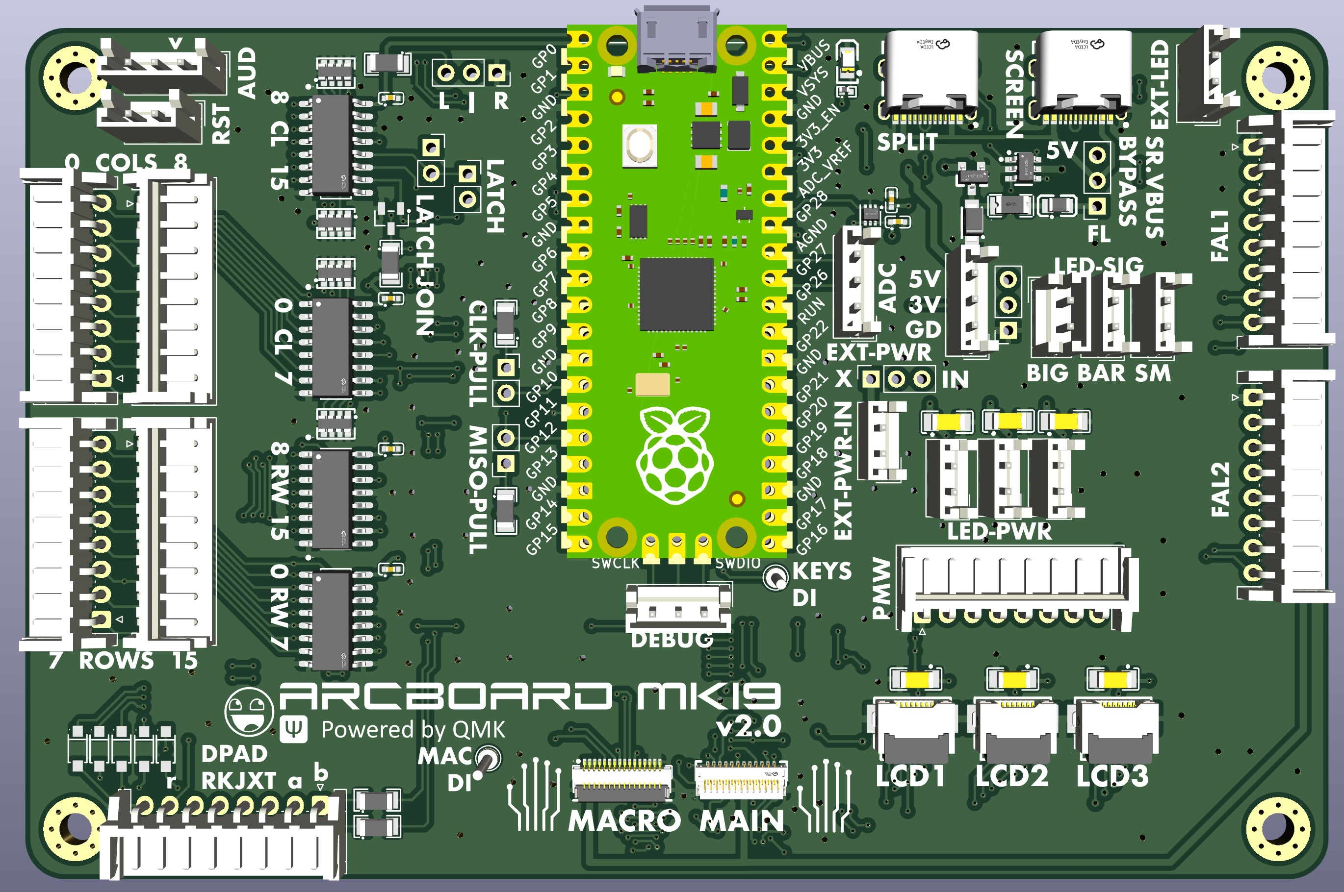
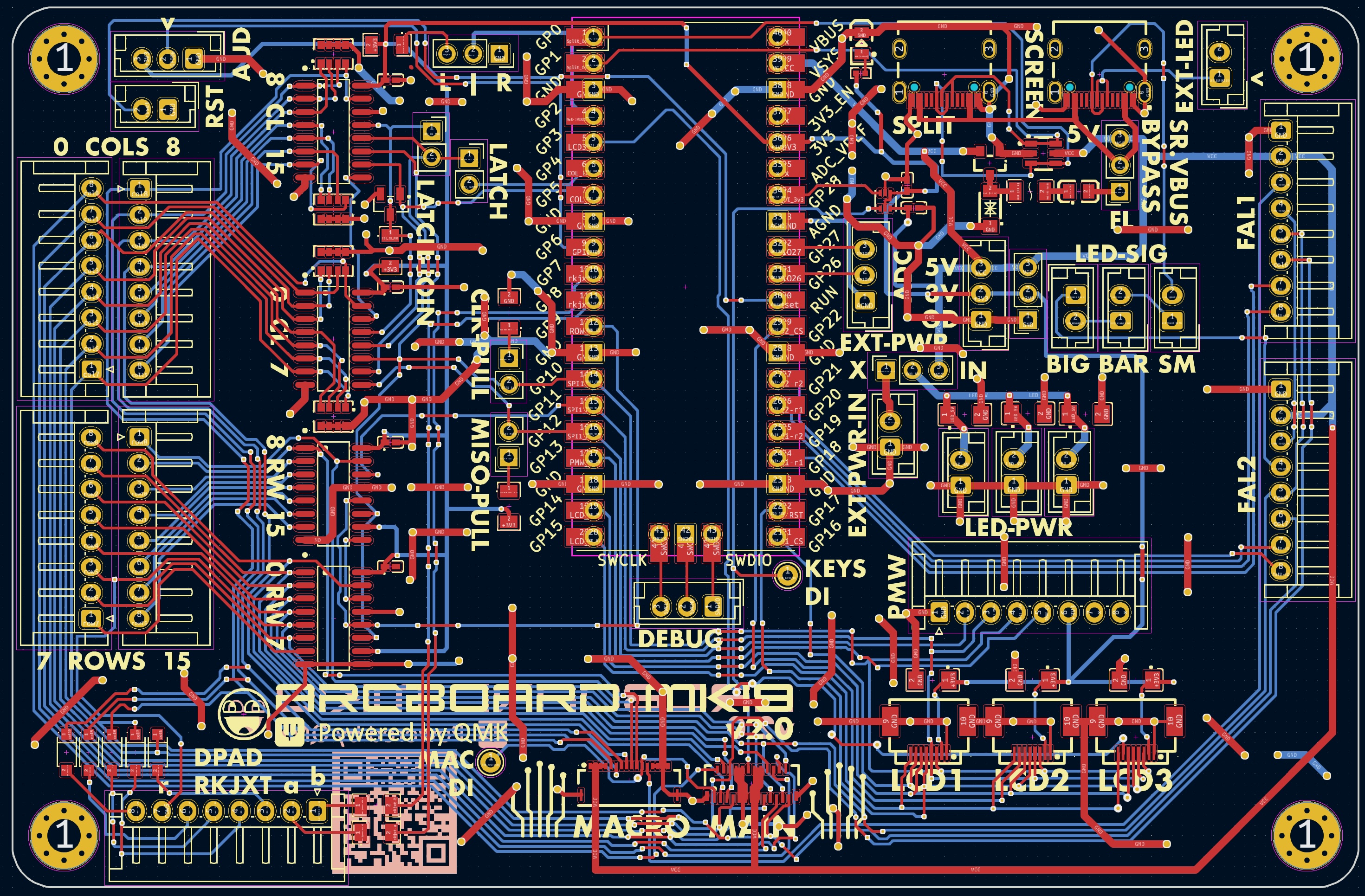
Mk19-pcb is an open-source printed circuit board by christrotter, from the christrotter/mk19-pcb repository on GitHub, published under the MIT licence. It is a 2-layer board of 130 × 85 mm with 90 parts on 110 nets, routed with 2,339 tracks and 462 vias.
It is built around the AZC199-04S-MS, CL31B105KBHNNNE and 4D03WGJ0103T5E, with the 74HC595D, TYPE-C-31-M-12 and ECT818001569 among its other parts. Its parts include 12 capacitors, 11 resistors, 9 ICs, 9 connectors and 2 diodes. It belongs with the RP2040 and NXP (LPC, Kinetis, i.MX RT) boards of this library.


The antithesis of 'keep it simple, stupid' - all the features, all the time.
Do you need...
...probably not, which is why I had to design my own pcb. So here it is...
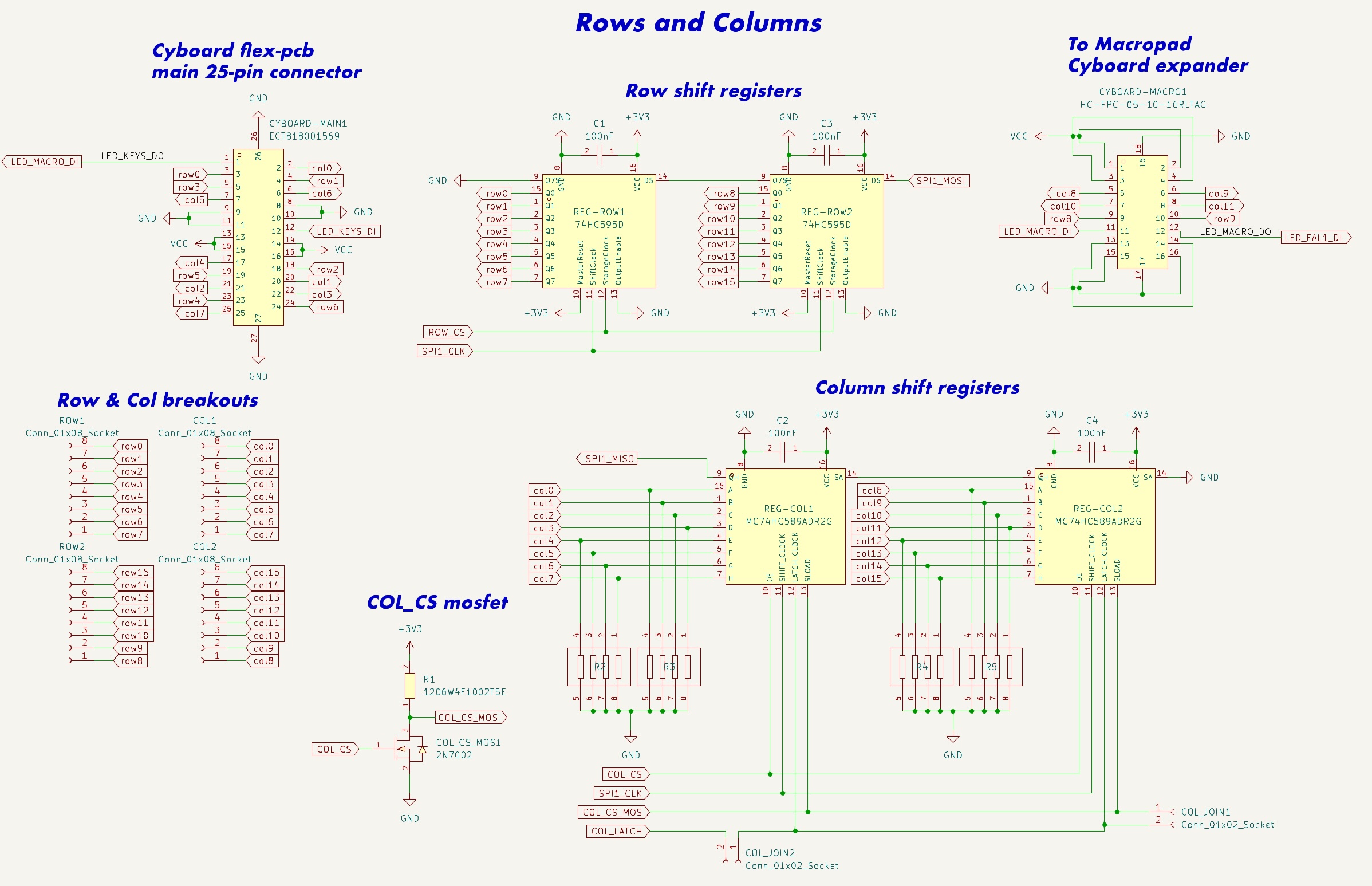
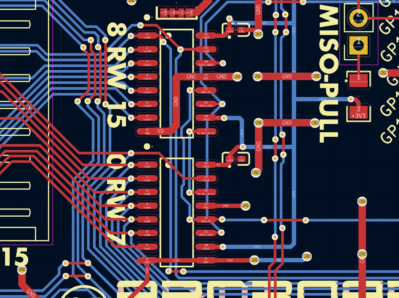
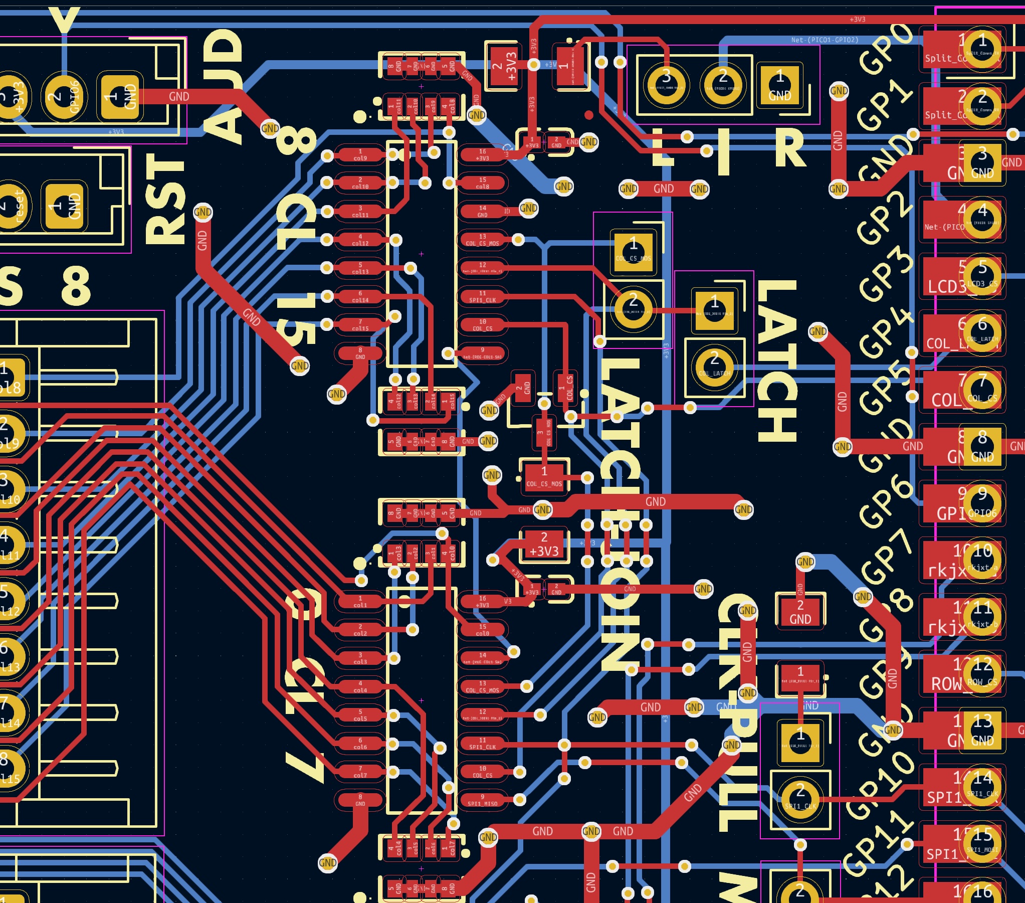
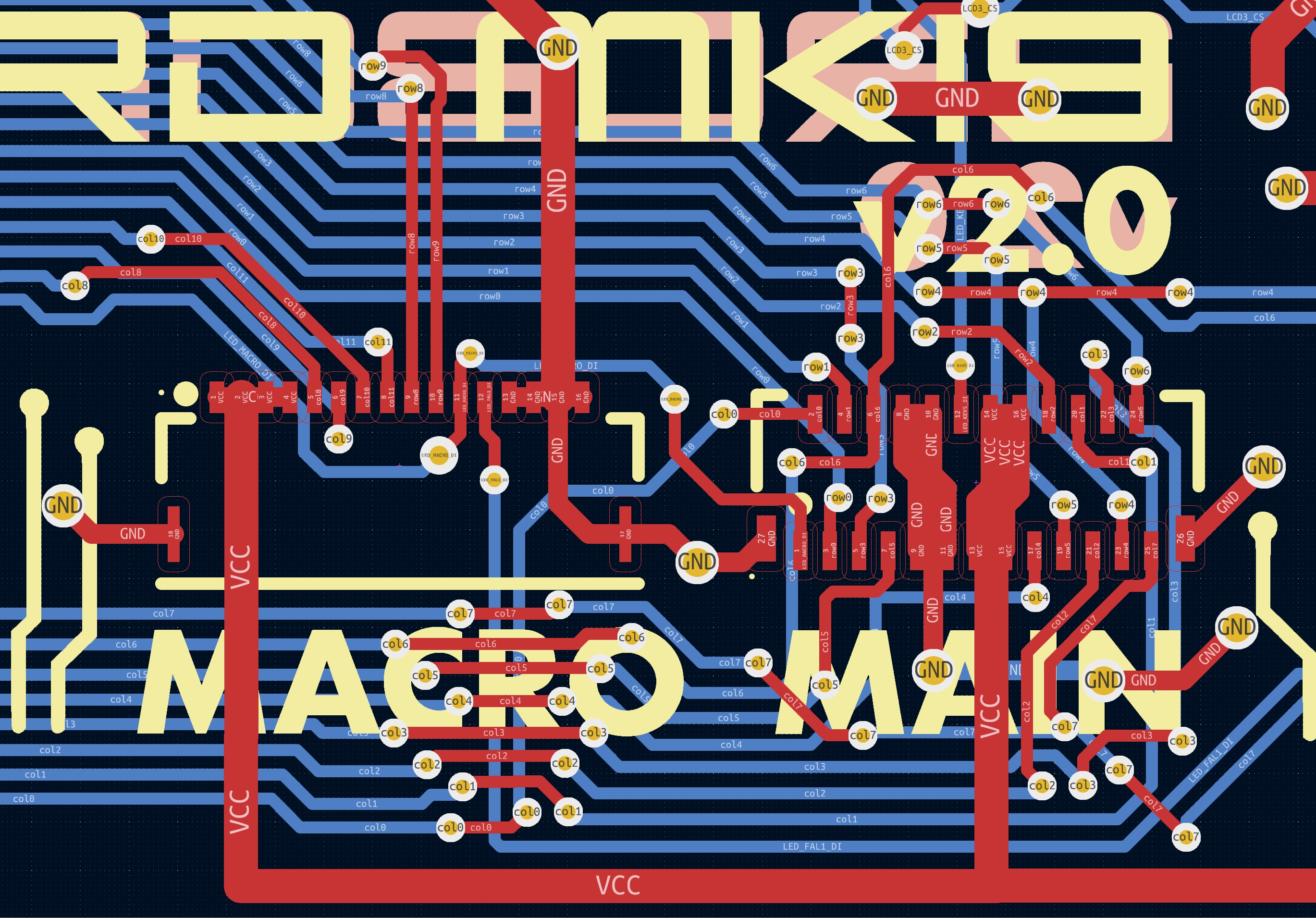
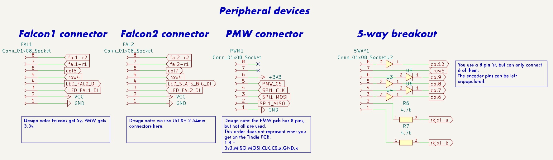
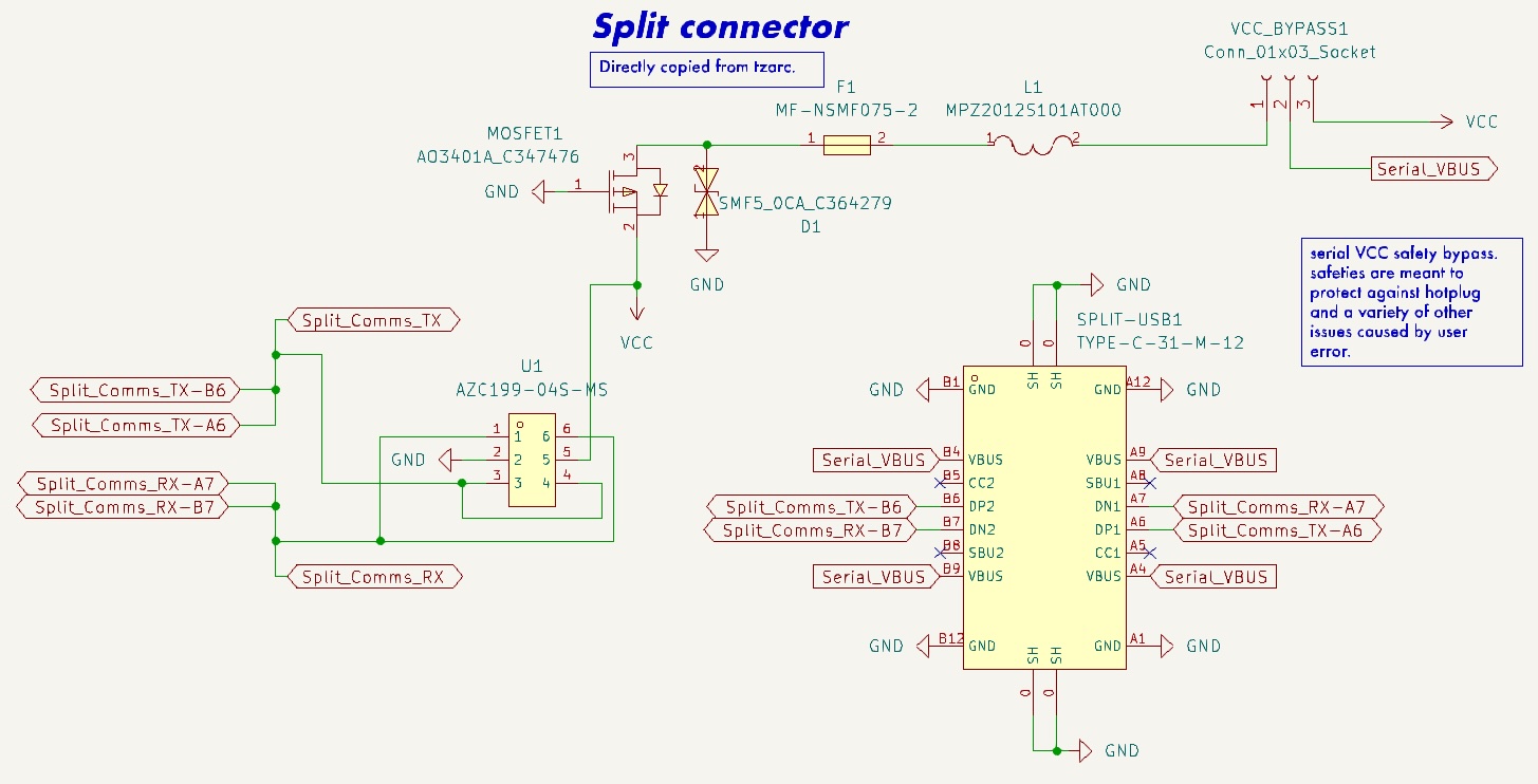
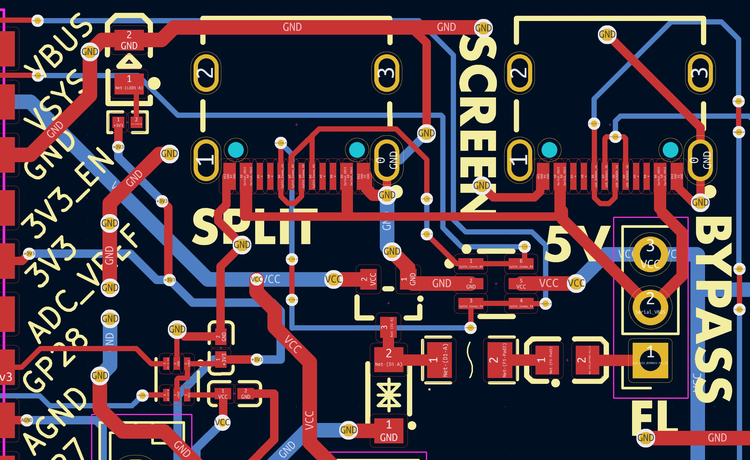
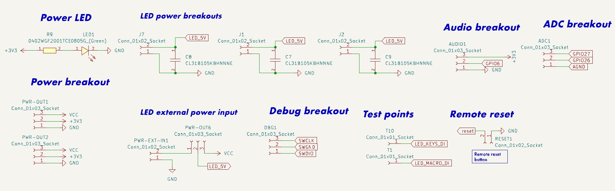
| Qty | Value | Footprint | References |
|---|---|---|---|
| 9 | Conn_01x02_Socket | Connector_JST:JST_EH_B2B-EH-A_1x02_P2.50mm_Vertical | J1, J2, J4, J7, J9, J10, J11, PWR-EXT-IN1, RESET1 |
| 8 | Conn_01x08_Socket | Connector_JST:JST_EH_S8B-EH_1x08_P2.50mm_Horizontal | 5WAY1, COL1, COL2, FAL1, FAL2, PWM1, ROW1, ROW2 |
| 6 | 100nF | ct-kicad:C0402 | C1, C2, C3, C4, C5, C6 |
| 6 | CL31B105KBHNNNE | ct-kicad:C1206 | C7, C8, C9, C10, C11, C12 |
| 5 | 1N4148W_C81598 | ct-kicad:SOD-123F_L2.7-W1.6-LS3.8-RD | U2, U3, U4, U5, U6 |
| 4 | 4D03WGJ0103T5E | ct-kicad:RES-ARRAY-SMD_0603-8P-L3.2-W1.6-BL | R2, R3, R4, R5 |
| 4 | Conn_01x02_Socket | Connector_PinSocket_2.54mm:PinSocket_1x02_P2.54mm_Vertical | CLK_PULL1, COL_JOIN1, COL_JOIN2, MISO_PULL1 |
| 4 | Conn_01x03_Socket | Connector_JST:JST_EH_B3B-EH-A_1x03_P2.50mm_Vertical | ADC1, AUDIO1, DBG1, PWR-OUT1 |
| 4 | Conn_01x03_Socket | Connector_PinSocket_2.54mm:PinSocket_1x03_P2.54mm_Vertical | PWR-OUT2, PWR-OUT6, SPLIT_HAND1, VCC_BYPASS1 |
| 4 | MountingHole | MountingHole:MountingHole_3.2mm_M3_Pad_Via | H1, H2, H3, H4 |
| 3 | 1206W4F1002T5E | ct-kicad:R1206 | R1, R10, R11 |
| 3 | 4.7k | ct-kicad:R1206 | R6, R7, R8 |
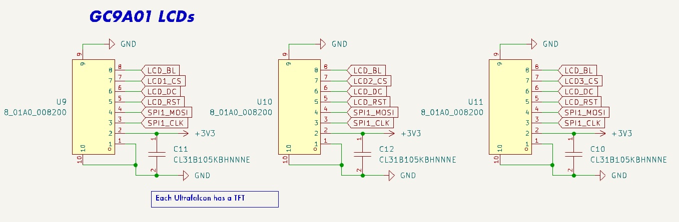
| 3 | 8_01A0_008200 | ct-kicad:FPC-SMD_8P-P0.50_8.01A0.008200 | U9, U10, U11 |
| 2 | **REF | ct-kicad:qmk-lite | LOGO2, LOGO4 |
| 2 | **REF | ct-kicad:awesome-logo | LOGO1, LOGO3 |
| 2 | **REF | ct-kicad:cyboard-logo-10mm | LOGO6, LOGO7 |
| 2 | 74HC595D | ct-kicad:SOIC-16_L9.9-W3.9-P1.27-LS6.0-BL | REG-ROW1, REG-ROW2 |
| 2 | Conn_01x01_Socket | Connector_Pin:Pin_D1.0mm_L10.0mm | T1, T10 |
| 2 | MC74HC589ADR2G | ct-kicad:SOIC-16_L9.9-W3.9-P1.27-LS6.0-BL | REG-COL1, REG-COL2 |
| 2 | TYPE-C-31-M-12 | ct-kicad:USB-C_SMD-TYPE-C-31-M-12 | SCREEN1, SPLIT-USB1 |
| 1 | **REF | ct-kicad:mk19-qr-logo-12mm | LOGO5 |
| 1 | 0402WGF2001TCE | ct-kicad:R0402 | R9 |
| 1 | 0805G_(Green) | ct-kicad:LED0805-R-RD | LED1 |
| 1 | 2N7002 | ct-kicad:SOT-23-3_L2.9-W1.3-P1.90-LS2.4-BR | COL_CS_MOS1 |
| 1 | AO3401A_C347476 | ct-kicad:SOT-23_L2.9-W1.3-P1.90-LS2.4-BR | MOSFET1 |
| 1 | AZC199-04S-MS | ct-kicad:TSOT-23-6_L2.9-W1.6-P0.95-LS2.8-BL | U1 |
| 1 | ECT818001569 | ct-kicad:FPC-SMD_ECT818001569 | CYBOARD-MAIN1 |
| 1 | HC-FPC-05-10-16RLTAG | ct-kicad:FPC-SMD_16P-P0.50_HCTL_HC-FPC-05-10-16RLTAG | CYBOARD-MACRO1 |
| 1 | MF-NSMF075-2 | ct-kicad:F1206 | F1 |
| 1 | MPZ2012S101AT000 | ct-kicad:L0805 | L1 |
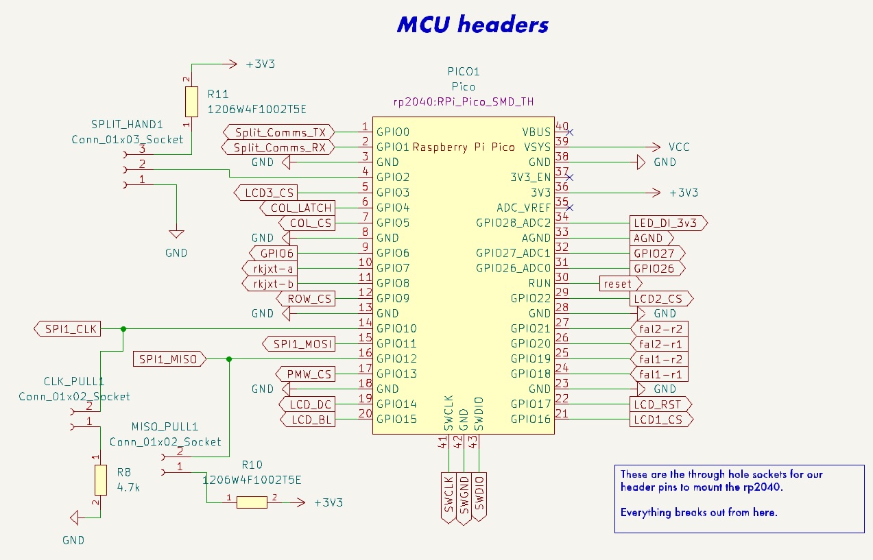
| 1 | Pico | rp2040:RPi_Pico_SMD_TH | PICO1 |
| 1 | SMF5_0CA_C364279 | ct-kicad:SOD-123FL_L2.8-W1.8-LS3.7-BI | D1 |
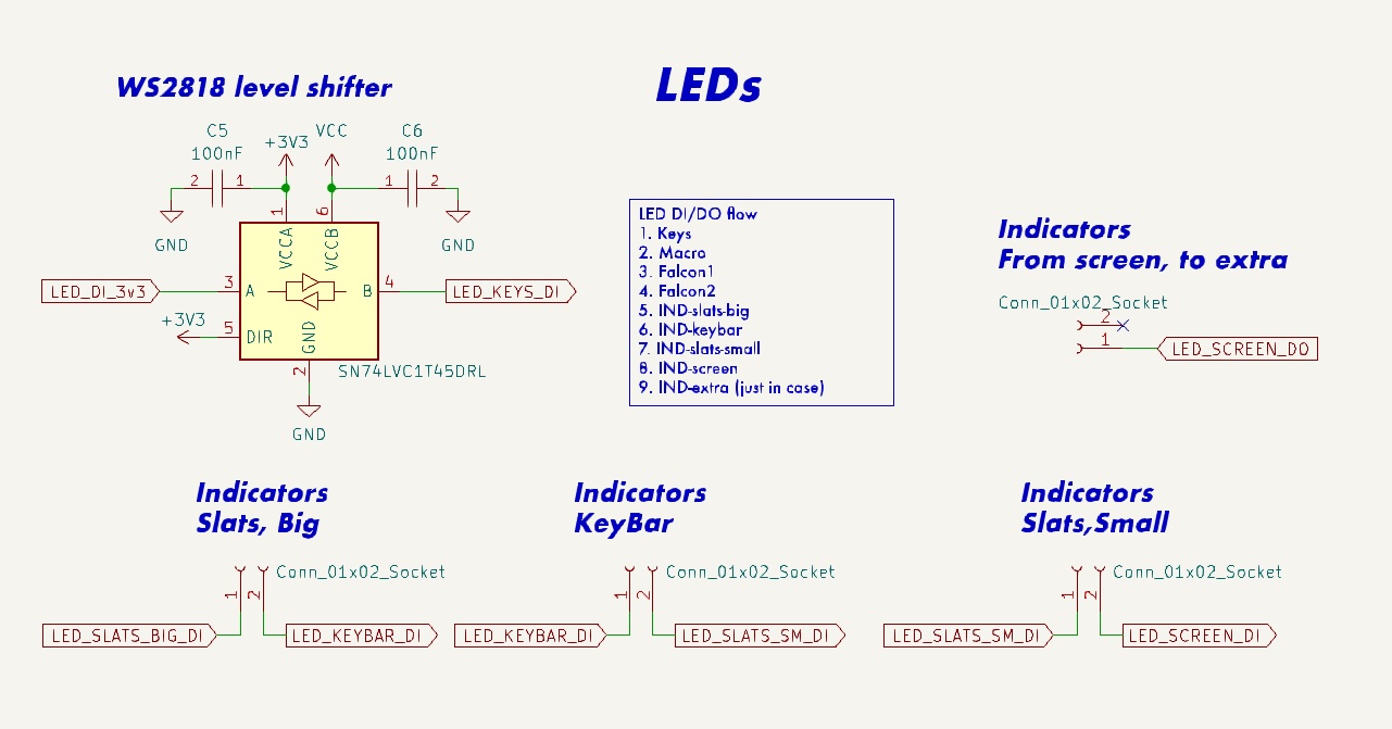
| 1 | SN74LVC1T45DRL | ct-kicad:SOT-563_L1.6-W1.2-P0.50-LS1.6-BR | LED-LVL1 |
christrotter/arcboard-stm32-mk2
Next iteration of the stm32f405 board; paradigm shift means new repo.


vaknin/PCB
Hardware ideas to fab-ready PCBs as code: Rust pcbgen on KiCad 10, Freerouting, ESP-IDF firmware with QEMU/Wokwi simulation, CadQuery enclosures

christrotter/shift-register-spi-breakout-pcb
Simple breakout board that gets you 16 rows and 16 cols for your QMK matrix.

sbarisic/MagMouse
Open source hall-effect based mouse - no mechanical contacts - no failure points

littlemanbuilds/Kids_Traffic_Light
Open-source KiCad traffic light STEM kit for learning LEDs, soldering, and ESP32 programming.

FujiNetWIFI/fujinet-hardware
Schematics and design files for FujiNet hardware

igorwolfs/modular-processing-hw
MCU Breakout board with Hirose BM28B connector
It measures 130 × 85 mm and has 2 copper layers, 1.6 mm thick.
90 parts, built around the AZC199-04S-MS, CL31B105KBHNNNE, 4D03WGJ0103T5E and 74HC595D. The full list of its parts is on this page, with links to each part's symbol and footprint where PCBKit's library has them.
From the christrotter/mk19-pcb repository on GitHub, at the commit this page was made from: the board is mk19-pcb.kicad_pcb and its schematic mk19-pcb.kicad_sch. PCBKit opens the board in the browser, with nothing to install.
Its repository publishes it under the MIT licence: you may reuse it on that licence's terms (keep the author's notice, and for a copyleft licence share your changes alike).