2 layers94 × 70 mm

 christopherking-ee/bench-power-supply
Adjustable 1.4-11.9V benchtop power supply. KiCad Design, JLCPCB fabriaction, full bring-up
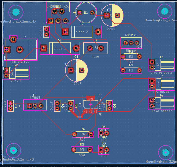
KiCad projects is an open-source printed circuit board by christopherking-ee, from the christopherking-ee/bench-power-supply repository on GitHub. It is a 2-layer board of 81.3 × 75.7 mm with 30 parts on 14 nets, routed with 94 tracks and 2 vias.
It is built around the LM2596S-ADJ, AMS1117-3.3 and L7805. Its parts include 7 capacitors, 4 resistors, 4 diodes, 4 connectors and 3 ICs. It belongs with the power boards of this library.


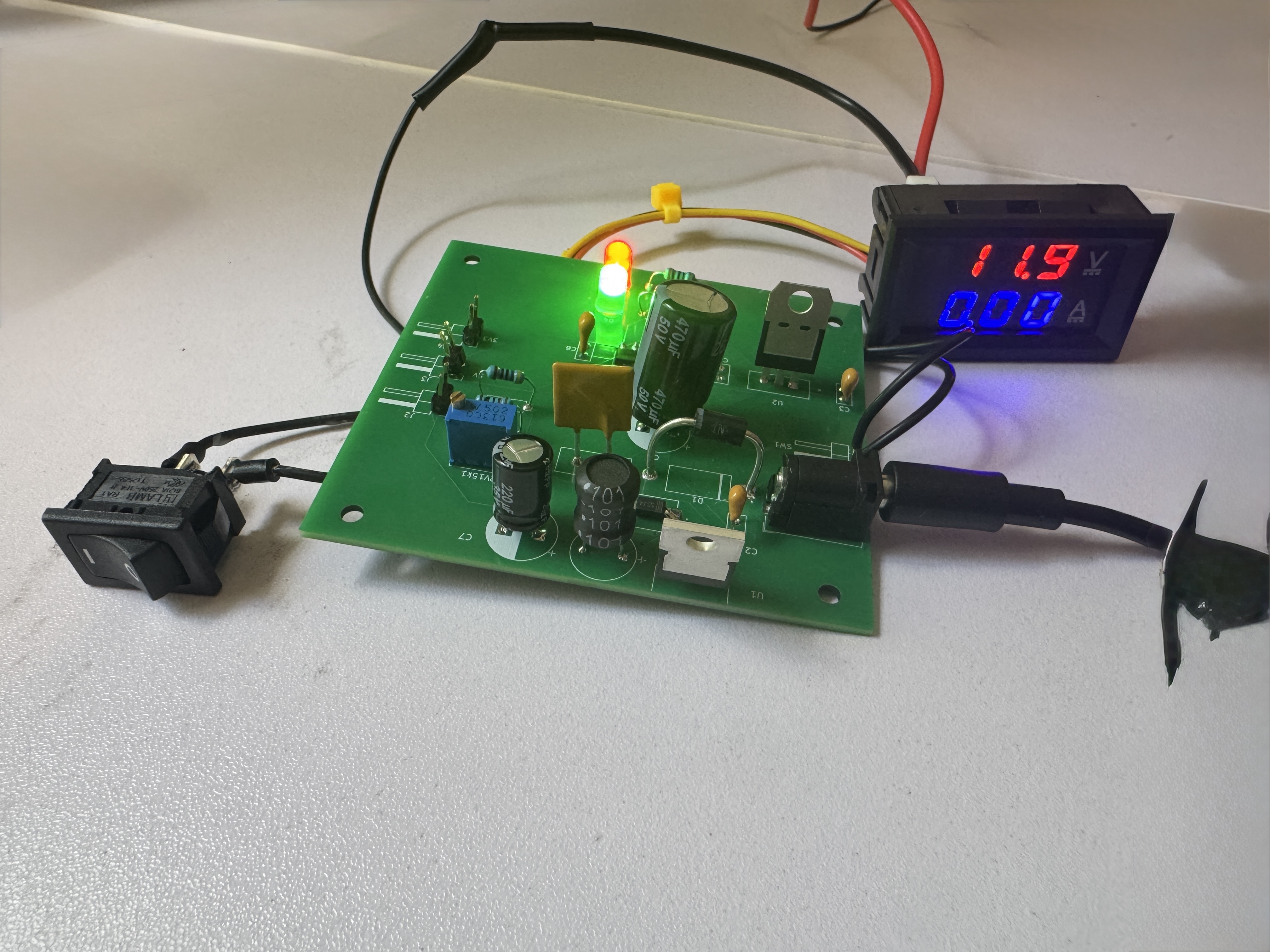
A from-scratch benchtop power supply: adjustable 1.4–11.9 V buck-regulated main output with live voltage/current display, plus fixed 5 V and 3.3 V rails. Designed in KiCad, fabricated by JLCPCB, hand-assembled, and brought up with a staged test procedure.
| Parameter | Value |
|---|---|
| Input | 12 V DC barrel jack (center-positive, regulated) |
| Adjustable output | 1.4 – 11.9 V (25-turn trimmer), ~2 A class |
| Fixed rails | 5.0 V (L7805) and 3.3 V (AMS1117) on headers |
| Metering | Panel voltmeter/ammeter on the adjustable output |
| Protection | Reverse-polarity Schottky (1N5822), 3 A resettable PTC fuse, per-rail decoupling |
Vout = 1.23 × (1 + R_upper/R_lower), with a 25-turn trimmer as the adjustable element.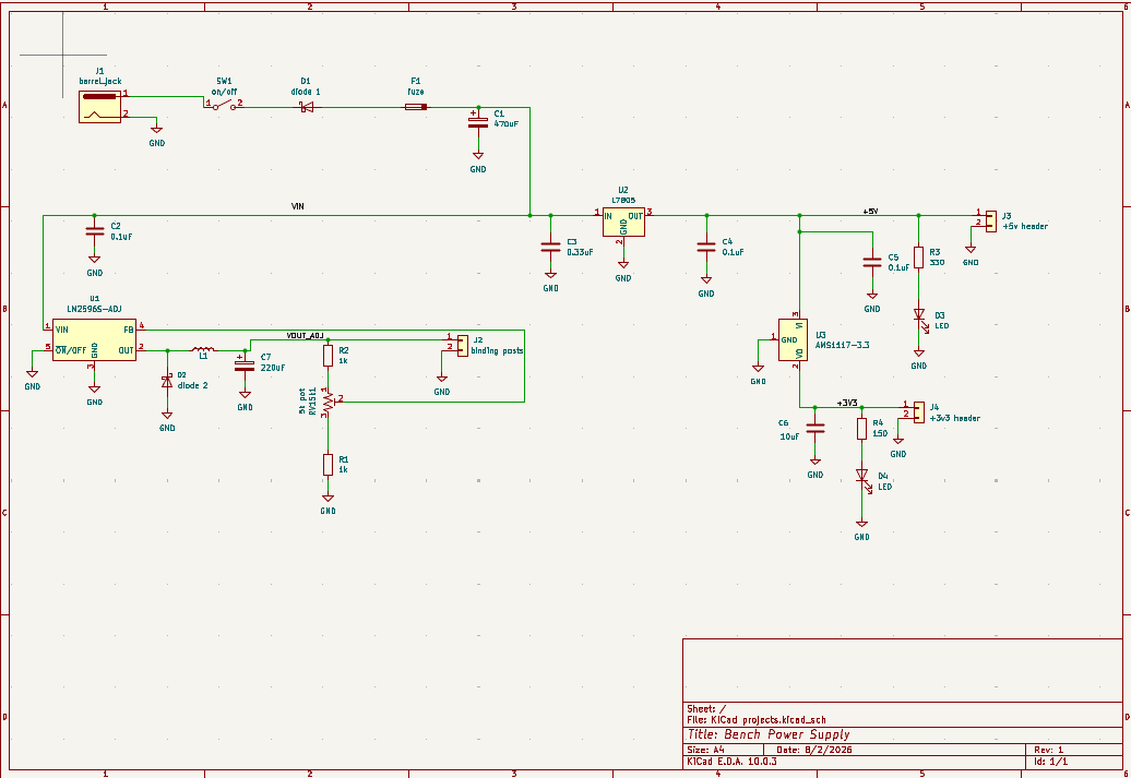
Every one of these was found by measurement during bring-up.
Staged and gated: visual inspection → continuity short-hunt on every rail → adapter verification → first power with no load, rail-by-rail measurement → potentiometer sweep across the full range → panel-meter cross-calibration against the DMM → first real load. No stage proceeds until the previous one passes.
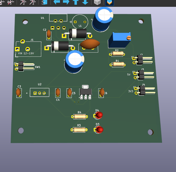
kicad/ — schematic and PCB sourcegerbers/ — fabrication files as sent to JLCPCBimages/ — renders and build photosThis supply's first load was my PID temperature controller — the panel ammeter visibly tracks the controller's PWM duty as it regulates.
| Qty | Value | Footprint | References |
|---|---|---|---|
| 4 | MountingHole_3.2mm_M3 | MountingHole:MountingHole_3.2mm_M3 | , , , |
| 3 | 0.1uF | Capacitor_THT:C_Disc_D5.0mm_W2.5mm_P2.50mm | C2, C4, C5 |
| 2 | 1k | Resistor_THT:R_Axial_DIN0207_L6.3mm_D2.5mm_P7.62mm_Horizontal | R1, R2 |
| 2 | LED | LED_THT:LED_D3.0mm | D3, D4 |
| 1 | +3v3 header | Connector_PinHeader_2.54mm:PinHeader_1x02_P2.54mm_Horizontal | J4 |
| 1 | +5v header | Connector_PinHeader_2.54mm:PinHeader_1x02_P2.54mm_Horizontal | J3 |
| 1 | 0.33uF | Capacitor_THT:C_Disc_D5.0mm_W2.5mm_P2.50mm | C3 |
| 1 | 10uF | Capacitor_THT:C_Disc_D5.0mm_W2.5mm_P2.50mm | C6 |
| 1 | 150 | Resistor_THT:R_Axial_DIN0207_L6.3mm_D2.5mm_P7.62mm_Horizontal | R4 |
| 1 | 220uF | Capacitor_THT:CP_Radial_D10.0mm_P5.00mm | C7 |
| 1 | 330 | Resistor_THT:R_Axial_DIN0207_L6.3mm_D2.5mm_P7.62mm_Horizontal | R3 |
| 1 | 470uF | Capacitor_THT:CP_Radial_D10.0mm_P5.00mm | C1 |
| 1 | 5k pot | Potentiometer_THT:Potentiometer_Bourns_3296W_Vertical | RV15k1 |
| 1 | AMS1117-3.3 | Package_TO_SOT_SMD:SOT-223-3_TabPin2 | U3 |
| 1 | L | myFootprints:IND_BOURNS_RLB0914 | L1 |
| 1 | L7805 | myFootprints:TO-220_STM | U2 |
| 1 | LM2596S-ADJ | myFootprints:T05D | U1 |
| 1 | barrel_jack | Connector_BarrelJack:BarrelJack_CUI_PJ-102AH_Horizontal | J1 |
| 1 | binding posts | Connector_PinHeader_2.54mm:PinHeader_1x02_P2.54mm_Horizontal | J2 |
| 1 | diode 1 | myFootprints:P2_DO-201 | D1 |
| 1 | diode 2 | myFootprints:P2_DO-201 | D2 |
| 1 | fuze | Capacitor_THT:C_Disc_D11.0mm_W5.0mm_P5.00mm | F1 |
| 1 | on/off | Connector_PinHeader_2.54mm:PinHeader_1x02_P2.54mm_Horizontal | SW1 |


getriscvyy/divesync-heavy
A syringe-actuated buoyancy control device developed at the Bio-Inspired Robotics and Controls Lab at University of Houston.

Henriquepr15/ESP32-Motor-RS232
Projeto de hardware com ESP32, RS232 e controle de motor

hetii/preheater
The controller supports multiple heating zones, thermocouple monitoring, fan control, and a modern web-based interface for managing the entire process directly from a browser.

ilomon10/embedded-totalizer-hour-meter
ESP32 engine hour meter & totalizer: firmware, SensorFrame protocol, Node host tools, KiCad PCB and a Deno device simulator

It measures 81.3 × 75.7 mm and has 2 copper layers, 1.6 mm thick.
30 parts, built around the LM2596S-ADJ, AMS1117-3.3 and L7805. The full list of its parts is on this page, with links to each part's symbol and footprint where PCBKit's library has them.
From the christopherking-ee/bench-power-supply repository on GitHub, at the commit this page was made from: the board is kicad/KiCad projects.kicad_pcb and its schematic kicad/KiCad projects.kicad_sch. PCBKit opens the board in the browser, with nothing to install.
Its repository states no licence, so its author keeps all rights: ask christopherking-ee before reusing the design.