
2 layers172 × 152.9 mm
 christopherdean11/DigitalLevel
Tie BOOT0 to GND for normal operation and programming with SWD. See this forum page. Could tie it to a resitor to GND to leave door open to overdrive it if needed for some reason.
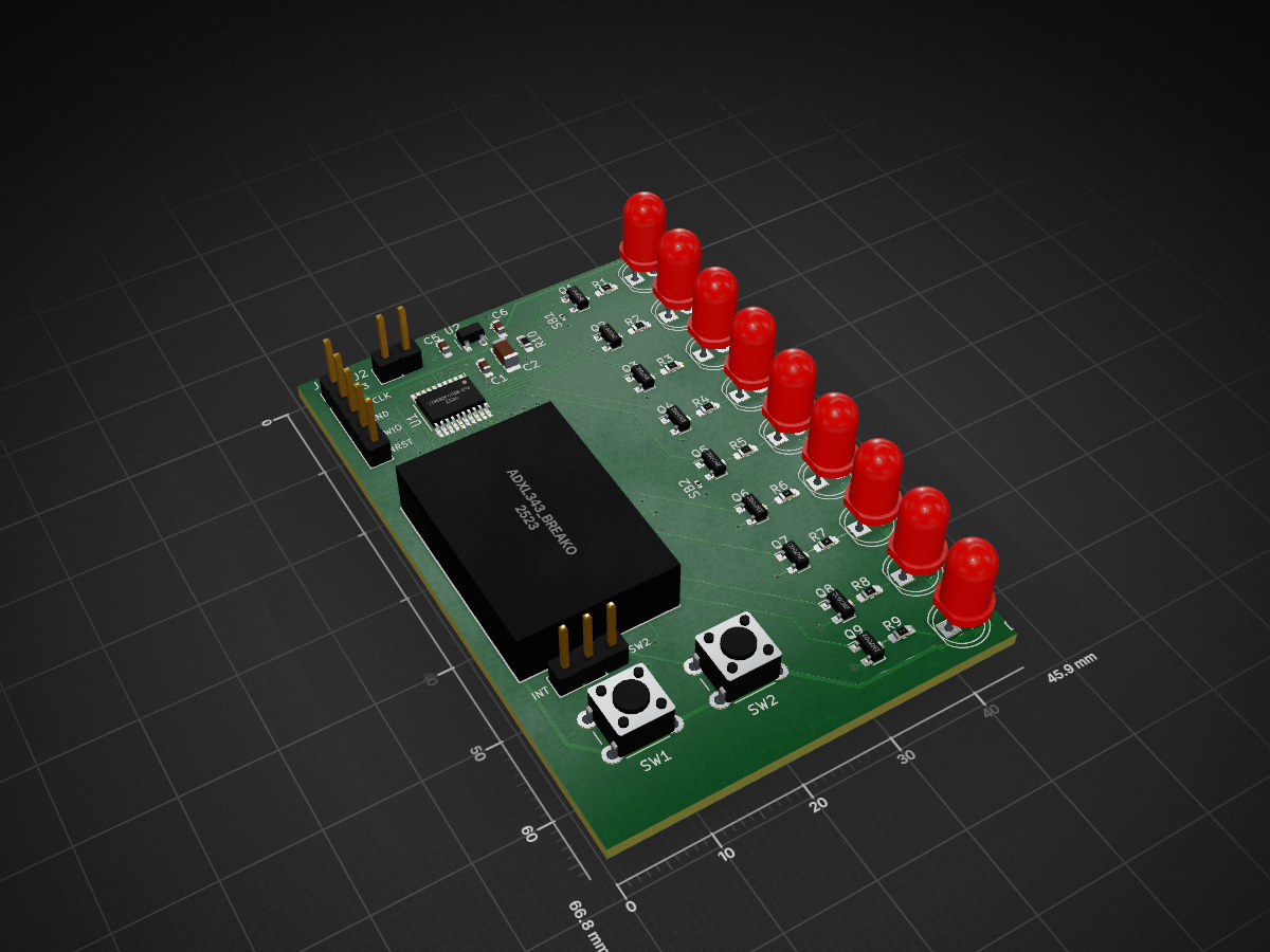
Led level pcb is an open-source printed circuit board by christopherdean11, from the christopherdean11/DigitalLevel repository on GitHub. It is a 2-layer board of 45.9 × 66.8 mm with 44 parts on 45 nets, routed with 310 tracks and 47 vias.
It is built around the MIC5504-3.3YM5. Its parts include 10 resistors, 9 diodes, 9 transistors, 6 capacitors and 3 ICs. It belongs with the STM32 boards of this library.
Initially thought about picking an STM32G0 series for low-cost, but after looking into it more, the STM32F0 series is not much more when buying low quantity, seems to be more popular, has extensive documentation, and the STM32F and STM32L series parts are already library components in Kicad.
Another considerations was a package that lends itself to hand soldering. With all of these in mind, I selected the STM32F030F4 in 20-pin TSSOP at approx. $1.23/unit.
This requires some time in STM Cube IDE to verify pinout and pin options to get a feel for what the board can look like. We can easily get 8 GPIO outputs for LEDs with this MCU. The STM32F030F4 comes in a 20pin TSSOP (this project will be hand soldered), with 12 GPIO available on PORTA + PB1 for 13 GPIO pins.
Another big item is how to program the MCU. It looks like the STM32F030F4 has SWD (I beleive all ARM MCUs have this) support, so I should be able to connect with ST-LINK using SWD pins. The F3 discovery board has an option to disconnect the actual dev board section from the ST-LINK section and use ST-LINK to program another board. This will be a good starting point for programming. So the board will need to have the SWD pins broken out to headers.
Tie BOOT0 to GND for normal operation and programming with SWD. See this forum page. Could tie it to a resitor to GND to leave door open to overdrive it if needed for some reason.
The pinout for the SWD connector on the F3 Discovery board is available in this document, page 16 Pins required:
Note: Eventually gave up with the F3 Discovery and orered a standalone ST-LINK V2 dongle, seems to just be easier
Plan is to power the board with 5V DC from a wall wart and regulate it to 3.3V. Since this isn't powered by a battery, power efficiency isn't really a concern on this project (save that futuer versions), so an LDO will be fine, gets the job done and is dead simple to add to a PCB.
Just filter on digikey/mouser for 3.3V LDO. Found MIC5504-3.3YM5 for 3.3V at 300mA and 2% initial accuracy. VIN up to 5.5V.
9 LEDs at 15mA = 135mA
Total allowed GPIO sourcing current for STM32F030F4 is 80mA (see page 44 in datasheet)
Redesigned board so LEDs are powered by the VDD rail and turned on off by GPIOs with an NMOS.
Needed a breakout board because all acceleromters have packages that do not lend themselves to hand-soldering. The ADXL343 breakout from Adafruit is reasonbly priced and uses a quality acceleromter. Some notes:
| SDO/ALT_ADDRESS Pin | 7 bit address | Read Address | Write Address |
|---|---|---|---|
| GND | 0x53 | 0xA6 | 0xA7 |
I2C address are 7-bit, and the least-signficant bit (LSB) is used to determine if the transaction is a read or write.
Begin layout of the design and revise as needed.
Populate minimally requried components to get a program onto the board and show a sign of life.
Once that is working populate remainder of board and run a progressive blink routine to validate each LED.
Eventually resolved these issues below and can talk to the board. Still not clear what the fix truly was, but I bought a standalone ST-LINK V2 USB dongle, updated STM CubeIDE to the latest, and completely discarded the Cube code project and started a Cube project, and all seems to be well. The program downloads to the micro and the debugger works. Original debugging notes kept here.
Error message from debugger back end:
Load failed
Failed to execute MI command:
load /Users/christopherdean/Dev/stm32/LED_Level/code/Debug/Digital_Level.elfError message from debugger back end:
Load failed
Load failed
Checked current on 3V3 rail (not using 3.3V regulator) and see it at ~1.3mA for a second or two, and then jump to ~1.8mA or 2mA
This schematic shows pullup/down resistors on SWCLKS/SWDIO
Command to run the debugger from command line: navigate to
/Applications/STM32CubeIDE.app/Contents/Eclipse/plugins/com.st.stm32cube.ide.mcu.externaltools.stlink-gdb-server.macos64_1.3.0.202002181050/tools/binand run
./ST-LINK_gdbserver -d -v -cp /Applications/STM32CubeIDE.app/Contents/Eclipse/plugins/com.st.stm32cube.ide.mcu.externaltools.cubeprogrammer.macos64_1.3.0.202002181050/tools/binWhen I run it to program my board:
STMicroelectronics ST-LINK GDB server. Version 5.5.0
Copyright (c) 2019, STMicroelectronics. All rights reserved.

Starting server with the following options:
        Persistent Mode            : Disabled
        Logging Level              : 31
        Listen Port Number         : 61234
        Status Refresh Delay       : 15s
        Verbose Mode               : Enabled
        SWD Debug                  : Enabled

Target connection mode: Default
Target connection failed. Try connecting under reset
Target connection failed
Target unknown error 19

Error in initializing ST-LINK device.
Reason: Unknown. Please check power and cabling to target.
When I install the jumpers on the F3DISCOVERY board to use the ST-LINK to program the discovery board (and not just as an ST-LINK for external things), I see this:
STMicroelectronics ST-LINK GDB server. Version 5.5.0
Copyright (c) 2019, STMicroelectronics. All rights reserved.

Starting server with the following options:
        Persistent Mode            : Disabled
        Logging Level              : 31
        Listen Port Number         : 61234
        Status Refresh Delay       : 15s
        Verbose Mode               : Enabled
        SWD Debug                  : Enabled

Target connection mode: Default
Hardware watchpoint supported by the target
COM frequency = 4000 kHz
ST-LINK Firmware version : V2J36M26
Device ID: 0x422
PC: 0x80007f8
ST-LINK device status: HALT_MODE
ST-LINK detects target voltage = 2.91 V
ST-LINK device status: HALT_MODE
ST-LINK device initialization OK
Waiting for debugger connection...
Waiting for connection on port 61234...
while it wait for a gdb process to connect to it
Maybe my microcontrollers are toasted? Maybe next step is to solder one to a breakout board and try to program it on a breadboard?
Borrowed an STM32 USB programmer from a friend, got a new error about part is LOCKUP and debugger timed out. Thought maybe finally clicking on the "Update CubeIDE" button might help. Get 1.4.2 installed and now the debugger won't even startup, just opens a window with
ST-LINK Server is required to start the debug session. Download from st.comOk. Download. Install. No change. Restart the IDE. No change. :( This forum post suggests downgrading from 1.4.2 to 1.4.0 to get it to work. Ugh. https://community.st.com/s/question/0D53W00000GWQKn/how-can-stlink-server-be-installed-for-use-by-stm32cubeide-
Tried to manually start the gdb session from the terminal with help here https://jacobmossberg.se/posts/2017/01/17/use-gdb-on-arm-assembly-program.html
it appeared to work and even saw ST-LINK device status: RUN_MODE but my board was still not working, perhaps a fundamental HW issue I just don't see.
NRST pin is tied to the NRST pin on the SWD jumper but otherwise is floating. It is supposed to be connected to a 40k ohm (typ) pullup internally. There is a recommendation for a 0.1uF external capacitor to prevent parasitic resets, which is missing from the PCB design.
Maybe try the i2c lines as usart data lines for programming? http://eleceng.dit.ie/frank/arm/STM32F030ISP/index.html
Maybe try after driving boot pin high: https://electronics.stackexchange.com/questions/410386/stm32f0-boot0-pin-and-swd-programming
| Qty | Value | Footprint | References |
|---|---|---|---|
| 9 | 2N7002 | Package_TO_SOT_SMD:SOT-23 | Q1, Q2, Q3, Q4, Q5, Q6, Q7, Q8, Q9 |
| 9 | LED | LED_THT:LED_D5.0mm | D1, D2, D3, D4, D5, D6, D7, D8, D9 |
| 8 | 100 | Resistor_SMD:R_0603_1608Metric_Pad1.05x0.95mm_HandSolder | R1, R2, R3, R4, R6, R7, R8, R9 |
| 2 | 0 | Resistor_SMD:R_0201_0603Metric | SB1, SB2 |
| 2 | 1u | Capacitor_SMD:C_0603_1608Metric_Pad1.05x0.95mm_HandSolder | C5, C6 |
| 2 | SW_Push | Button_Switch_THT:SW_PUSH_6mm | SW1, SW2 |
| 1 | 100n | Capacitor_SMD:C_0603_1608Metric_Pad1.05x0.95mm_HandSolder | C1 |
| 1 | 10n | Capacitor_SMD:C_0603_1608Metric_Pad1.05x0.95mm_HandSolder | C3 |
| 1 | 1u | Capacitor_SMD:C_1206_3216Metric_Pad1.42x1.75mm_HandSolder | C4 |
| 1 | 4.7u | Capacitor_SMD:C_1206_3216Metric_Pad1.42x1.75mm_HandSolder | C2 |
| 1 | 82 | Resistor_SMD:R_0603_1608Metric_Pad1.05x0.95mm_HandSolder | R5 |
| 1 | ADXL343_Breakout | footprints:ADXL343_Breakout | U3 |
| 1 | Conn_SWD | Connector_PinHeader_2.54mm:PinHeader_1x05_P2.54mm_Vertical | J1 |
| 1 | Conn_SW_INT | Connector_PinHeader_2.54mm:PinHeader_1x03_P2.54mm_Vertical | J3 |
| 1 | Conn_VIN | Connector_PinHeader_2.54mm:PinHeader_1x02_P2.54mm_Vertical | J2 |
| 1 | MIC5504-3.3YM5 | Package_TO_SOT_SMD:SOT-23-5 | U2 |
| 1 | R | Resistor_SMD:R_0603_1608Metric_Pad1.05x0.95mm_HandSolder | R10 |
| 1 | STM32F030F4Px | Package_SO:TSSOP-20_4.4x6.5mm_P0.65mm | U1 |
It measures 45.9 × 66.8 mm and has 2 copper layers, 1.6 mm thick.
44 parts, built around the MIC5504-3.3YM5. The full list of its parts is on this page, with links to each part's symbol and footprint where PCBKit's library has them.
From the christopherdean11/DigitalLevel repository on GitHub, at the commit this page was made from: the board is pcb/led_level_pcb.kicad_pcb. PCBKit opens the board in the browser, with nothing to install.
Its repository states no licence, so its author keeps all rights: ask christopherdean11 before reusing the design.

tmk/USB2USB_Converter
USB to USB keyboard protocol converter supported by TMK keyboard firmware

kiu/lofence
LoFence is a LoRaWAN capable IoT electric fence monitoring system running on the The Things Network.


nkrackow/SingularitySurfer-FPGA-Lock-In-Amplifier
Repository for the development of an FPGA based DSP Lock-In Amplifier

AndersBNielsen/PhaseLatchMini
High-rate continuous streaming of interleaved dual ADC (I/Q) samples over USB Full‑Speed (FS) using only the built‑in CDC class on an STM32F103C8 ("Blue Pill" style) board.

Badbird5907/thermal-camera
My design of a cheap and affordable thermal camera

felixheld/qspimux
QSPI flash multiplexer - connect a SPI NOR flash to either an embedded system or a programmer for remote firmware tests