Skip to the content
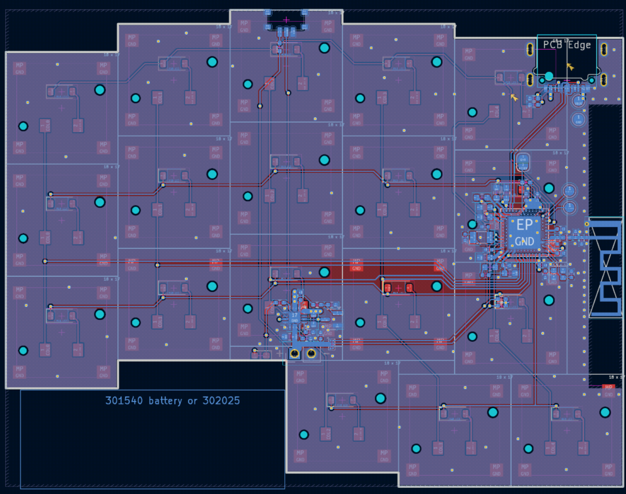
4 layers93.5 × 72.3 mmLeptosis left, the printed circuit board in 3D

Leptosis left

cheyao/leptosis60

Ultra flat PG1316 bluetooth split keyboard

Size
93.5 × 72.3 mm
Copper layers
4
Thickness
1.14 mm
Parts
91
Nets
100
Pads
414
Tracks, vias
550, 205
Pours
12
Routed
Yes
KiCad
KiCad 9.0 (file 20241229)
Created
23 Jun 2025
Updated
22 Jan 2026

Overview

Leptosis left is an open-source printed circuit board by cheyao, from the cheyao/leptosis repository on GitHub. It is a 4-layer board of 93.5 × 72.3 mm with 91 parts on 100 nets, routed with 550 tracks and 205 vias.

It is built around the BQ24075RGT, MAX17048X+T10 and 1N4148W. Its parts include 23 capacitors, 19 diodes, 19 switches, 12 resistors and 4 inductors. It belongs with the keyboards and input boards and the nRF52 and nRF5x boards of this library.

Main components

3

README

README.md

Leptosis - Ultra Flat PG1316 Split Keyboard

"Leptos" stands for "flat" in greek, added with the suffix is, it forms the word "Leptosis", signifying the most flat. This represents my long lasting desire for an real flat keyboard that is portable and light. The name is also quite similar to the latin word "levitatio", signifying levitation and thus light. (I'm bad at naming things lol)

What is this?

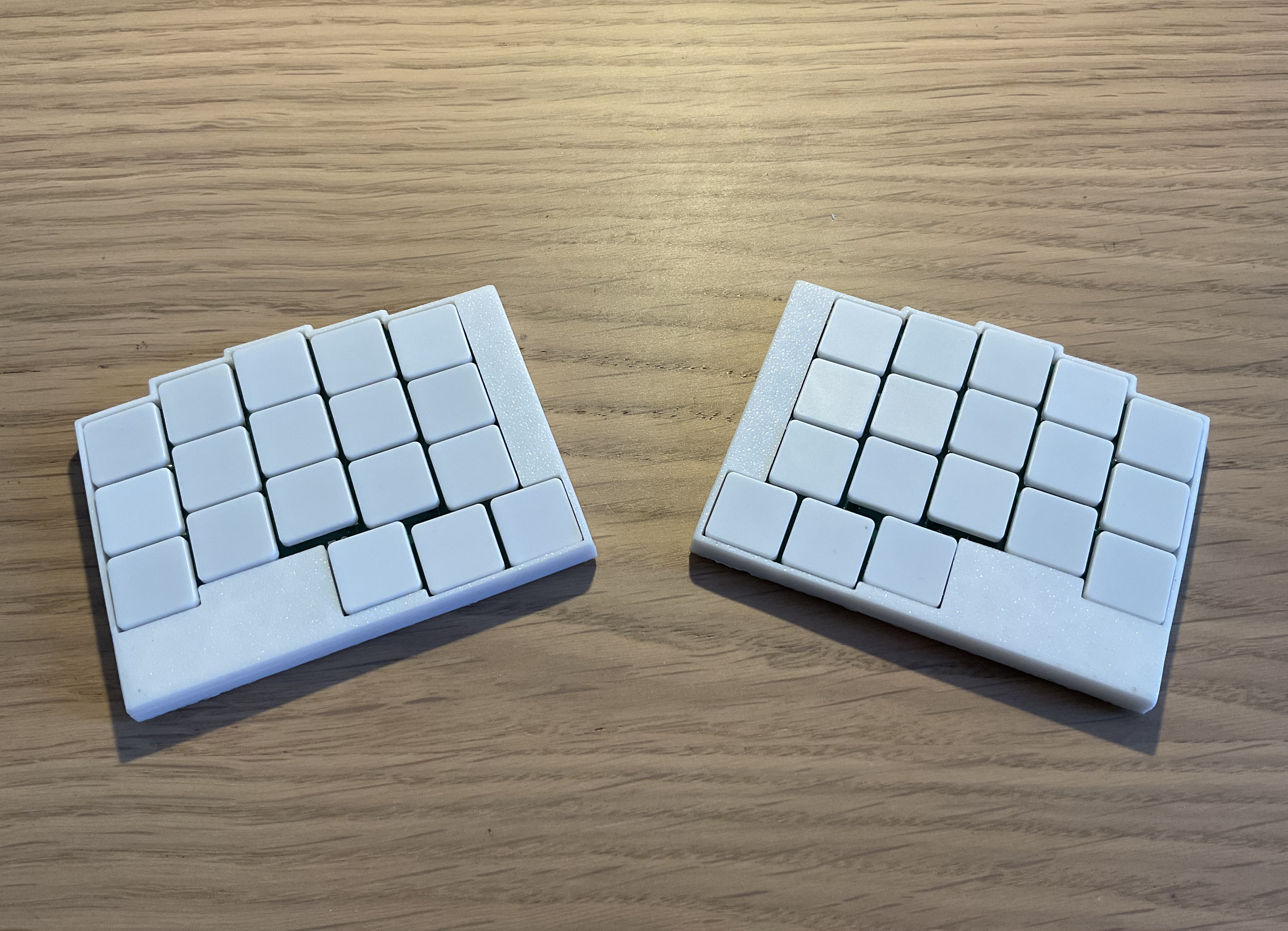
Leptosis is an ultra flat split bluetooth keyboard. It's thickness will be ~7.5mm, and employs the compact miryoku layout. Using an onboard nrf module, it achieves an ultra long battery life.

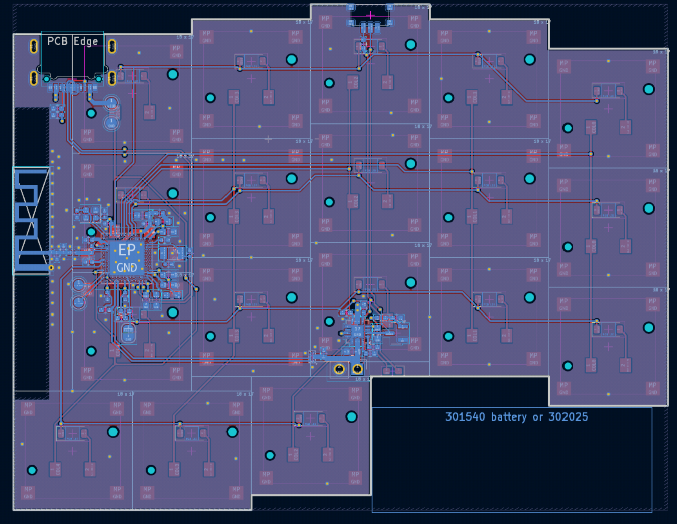
LeftRight

Features

  • Ultra long battery life (~4 months for central and 1 year for peripheral)
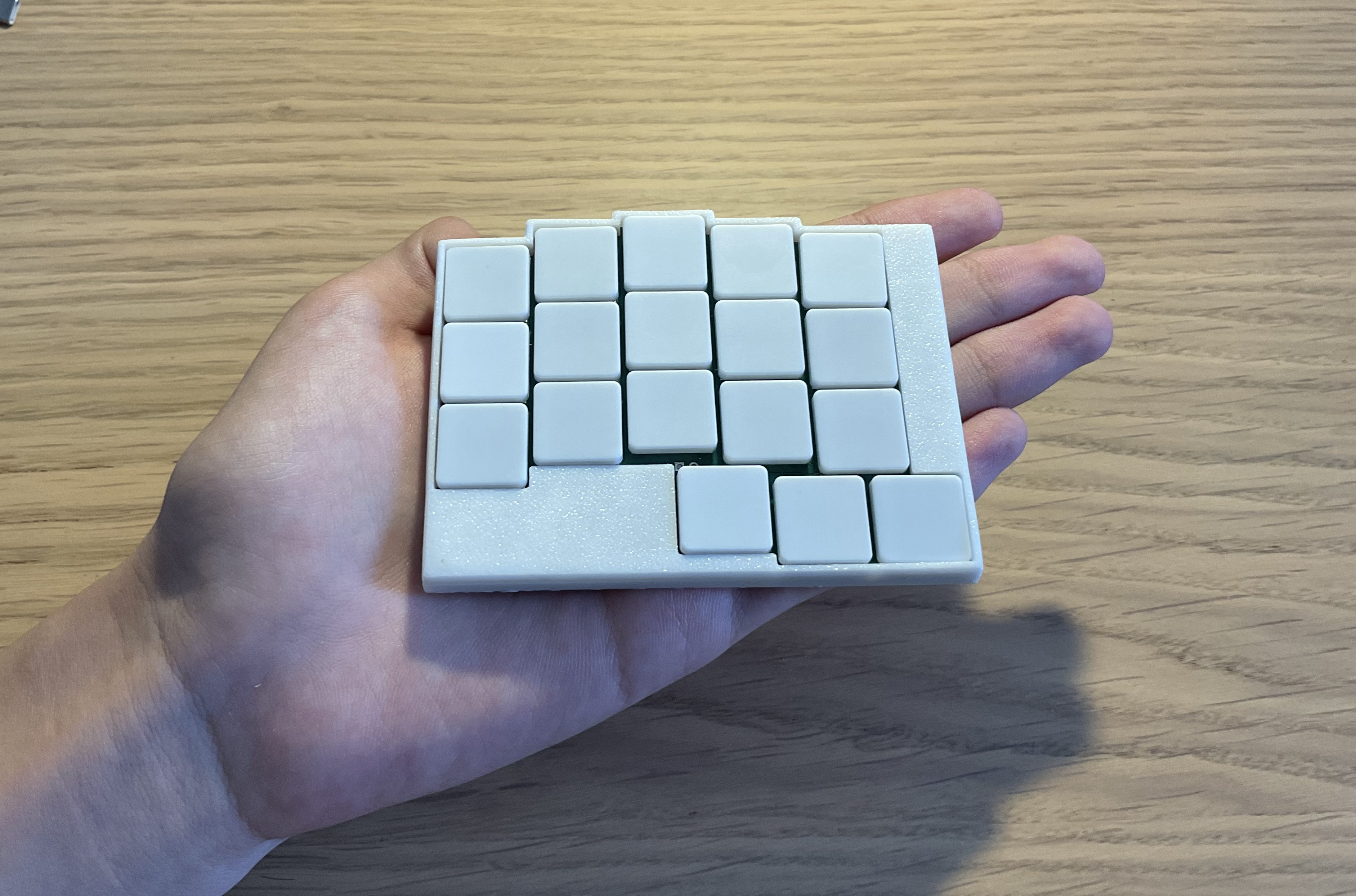
  • Ultra thin (7.5mm)
  • Compact (13.2x9.2cm)
  • Custom battery management and optimization
  • Embedded nrf52 mcu
  • ZMK bluetooth

Fabrication

You can either use PCBA to fabricate the PCB, or reflow it yourself. I highly discurrage you to reflow the yourself if you haven't reflowed a aQFN package before - it's a nightmare to get right.

The PCB files are in the hardware directory, you need to buy one pcb for the right and the left. There is also a V-Cut panneled version in hardware/panel. It uses JLCPCB's 1.2mm JLC04121H-7628 stackup. Other stackups would require re-tuning of the USB data lines and antenna feed trace.

The case is in the CAD directory. Print out all .step files.

The software is in the firmware. Leptosis uses ZMK, allowing ultra long battery life.

After fabrication, solder on some jumpers onto the 4 test pads, and connect it to a JTAG connector (I'm using the ST-LINK). Download the bootloader from the newest action here and unzip it.

For stlink, install openocd and run the following commands:

zsh
openocd -f /usr/share/openocd/scripts/interface/stlink.cfg -f /usr/share/openocd/scripts/target/nrf52.cfg -c 'program <path_to_bootloader>.hex verify reset; shutdown;'

For other JTAG connectors, please refer to your own documentation.

Now plug in a USB-C cable, and you should see a mass storage device called LEPTOSIS.

Download the ZMK config from this repo: https://github.com/cheyao/zmk-config/actions, drag the utf file to the mass storage device and you are done!

Misc

Liked this project? Drop a star and check out my other Icepi Zero project!

Parts

91
QtyValueFootprintReferences
181N4148WDiode_SMD:D_SOD-123D1, D2, D3, D4, D5, D7, D10, D11, D13, D14, D15, D16, D17, D21, D22, D23 +2
18SW_PushPCM_marbastlib-xp-choc:SW_PG1316SSW2, SW3, SW4, SW5, SW6, SW10, SW11, SW12, SW14, SW15, SW16, SW17, SW18, SW22, SW23, SW24 +2
64.7uFCapacitor_SMD:C_0603_1608MetricC13, C14, C15, C16, C21, C22
5100nFCapacitor_SMD:C_0402_1005MetricC8, C18, C19, C20, C23
410kResistor_SMD:R_0402_1005Metric_Pad0.72x0.64mm_HandSolderR3, R6, R8, R10
415pFCapacitor_SMD:C_0402_1005MetricC1, C2, C3, C4
45.1kResistor_SMD:R_0402_1005Metric_Pad0.72x0.64mm_HandSolderR1, R2, R15, R16
4TestPointTestPoint:TestPoint_Pad_D1.5mmTP1, TP2, TP3, TP4
21.5kResistor_SMD:R_0402_1005Metric_Pad0.72x0.64mm_HandSolderR5, R9
210uHInductor_SMD:L_0603_1608MetricL2, L4
21uFCapacitor_SMD:C_0603_1608MetricC11, C17
10.5pFCapacitor_SMD:C_0402_1005MetricC6
10.8pFCapacitor_SMD:C_0402_1005MetricC5
1100Resistor_SMD:R_0402_1005Metric_Pad0.72x0.64mm_HandSolderR7
1100pFCapacitor_SMD:C_0402_1005MetricC9
115nHInductor_SMD:L_0402_1005MetricL3
12N7002Package_TO_SOT_SMD:SOT-23Q2
13.9kResistor_SMD:R_0402_1005Metric_Pad0.72x0.64mm_HandSolderR4
132.768kHz 12.5pFCrystal:Crystal_SMD_3215-2Pin_3.2x1.5mmY2
132MHz 12pFCrystal:Crystal_SMD_2016-4Pin_2.0x1.6mmY1
14.7nHInductor_SMD:L_0402_1005MetricL1
147nFCapacitor_SMD:C_0402_1005MetricC12
1820pFCapacitor_SMD:C_0402_1005MetricC10
1Antenna_ShieldRF_Antenna:Texas_SWRA117D_2.4GHz_LeftAE1
1BQ24075RGTPackage_DFN_QFN:VQFN-16-1EP_3x3mm_P0.5mm_EP1.6x1.6mmU2
1Conn_01x02Connector_PinSocket_2.54mm:PinSocket_1x02_P2.54mm_VerticalJ2
1LEDLED_SMD:LED_0603_1608Metric_Pad1.05x0.95mm_HandSolderD31
1MAX17048Xleptosis:WLP-8_1.67x0.93_P0.4U3
1NCCapacitor_SMD:C_0402_1005MetricC7
1SW_SPDTleptosis:Switch_Sink_MINI_MSK12CO2SW31
1SolderJumper_2_OpenJumper:SolderJumper-2_P1.3mm_Open_RoundedPad1.0x1.5mmJP1
1USB_C_Receptacle_USB2.0_14PPCM_marbastlib-various:USB_C_Receptacle_HRO_TYPE-C-31-M-14J1
1nRF52840Package_DFN_QFN:Nordic_AQFN-73-1EP_7x7mm_P0.5mmU1

Similar boards

  • 4 layers33.1 × 32.2 mmLED Earrings Charging Board, the printed circuit board in 3D

    LED Earrings Charging Board

    sandgum/Triangulate-MS_01-Matrix-LED-Studs

    Tiny 8x8mm ear studs (inspired by Mitxela) with 16 LEDs on each, arranged in a 4x4 matrix. Each matrix is controlled by a MAX32660 microcontroller paired with an accelerometer to react to orientation changes.

    112 parts
  • 2 layers111 × 39.5 mmAddon panel, the printed circuit board in 3D

    Addon panel

    NotARealDevOrDesigner/rs1_pcb

    116 parts
  • 2 layers225.5 × 185.2 mmLevels, the printed circuit board in 3D

    Levels

    Good-Great-Grand-Wonderful/levels54

    Levels54 is for people who care about how things are made and how they feel. Every component—from ceramic trackball bearings to stainless switch plates—is chosen to deliver smooth, precise, durable performance.

    243 parts67MIT
  • 4 layers330.5 × 126.6 mmModular keyboard, the printed circuit board in 3D

    Modular keyboard

    cubit010/cubitboard

    This project is a keyboard that has the potential to have many different modules attached, modules such as displays, a rotary encoder panel, potentiometers, or a numpad! > [!NOTE] > Most of the features can be added due…

    204 parts1
  • 4 layers158.5 × 81.5 mmBiro-1-rev-0, the printed circuit board in 3D

    Biro-1-rev-0

    PROJECT-BIRO/Biro-1

    137 parts1MIT
  • 2 layers326.6 × 123.8 mmFreedom, the printed circuit board in 3D

    Freedom

    DynamicWhiteHat/Arc

    A Wireless 75% Backlit Keyboard

    421 parts
  • 4 layers76.2 × 66 mmRtk, the printed circuit board in 3D

    Rtk

    GM4AJK/gps-staff

    Surveyors GPS Staff - GPS/RTK Staff Positioning

    91 partsMIT
  • 2 layers179.8 × 116.7 mmAloidia right, the printed circuit board in 3D

    Aloidia right

    hRake/aloidia-keyboard

    Aloidia wireless split mechanical keyboard.

    227 parts

Questions

How big is the Leptosis left PCB?

It measures 93.5 × 72.3 mm and has 4 copper layers, 1.14 mm thick.

What parts does the Leptosis left use?

91 parts, built around the BQ24075RGT, MAX17048X+T10 and 1N4148W. The full list of its parts is on this page, with links to each part's symbol and footprint where PCBKit's library has them.

Where can I download the Leptosis left KiCad files?

From the cheyao/leptosis repository on GitHub, at the commit this page was made from: the board is hardware/left/leptosis-left.kicad_pcb and its schematic hardware/left/leptosis-left.kicad_sch. PCBKit opens the board in the browser, with nothing to install.

Can I use the Leptosis left design in my own project?

Its repository states no licence, so its author keeps all rights: ask cheyao before reusing the design.