2 layers82.5 × 127 mm
Power supply
nunosousa/SCART-switcher
An old school SCART switcher. Its main purpose will be to automaticaly detect and switch the video output to the active input video source.
59 parts

 ChengminLi/AI-PCB-layout31
AI agent skill for designing and reviewing power-electronics PCBs, with a human review gate after every step
Emc flyback is an open-source printed circuit board by ChengminLi, from the ChengminLi/AI-PCB-layout repository on GitHub, published under the CC-BY-4.0 licence. It is a 2-layer board of 100 × 76 mm with 90 parts on 40 nets, routed with 359 tracks and 155 vias.
It is built around the UC3845B, L78L12ACUTR-CN and LTV-817S, with the TL431AIDBZR, CC0603KRX7R9BB104 and CC1206KKX7RCBB103 among its other parts. Its parts include 24 capacitors, 20 resistors, 6 diodes, 5 connectors and 4 ICs.


 A gift for hardware engineer.
An AI agent skill for designing, reviewing, and improving power-electronics PCBs. This skill does not produce a PCB at the first try, instead it provides a way of how to collobrate with the AI agents to boost the productivity of PCB layout. I expect that the user has at least midlevel hardware experience, thus can provide engineering judgement to review the results.
The skill teaches an AI coding agent (Cursor, Claude Code, Codex, or any agent that supports SKILL.md skills) to work like a careful power-electronics layout engineer: it traces commutation and gate loops from the switching states, derives clearance and copper limits from standards and design currents, and stops for your approval after every step, so you stay in control of every design decision.
Note: The skill helps you reach a well-reasoned design and tells you which evidence is still missing. It does not certify safety or EMC compliance. Measurements and the applicable standards remain the final authority.
It works with any topology, device technology (Si, IGBT, SiC, GaN), and CAD tool. KiCad 9 is covered in the most detail; concept mappings are included for Altium Designer, Allegro/OrCAD, Xpedition/PADS, and Fusion.
The agent works in nine steps. After each step it delivers a short report and waits for you to reply approve, approve with changes, redo, or stop.
flowchart TD
    S1["1. Requirements and inputs"] -- gate --> S2["2. Architecture and limits"]
    S2 -- gate --> S3["3. Circuit and models<br/>(end-to-end only)"]
    S3 -- gate --> S4["4. Schematic, footprints, and 3D"]
    S4 -- gate --> S5["5. Design rules and stack-up"]
    S5 -- gate --> S6["6. Placement"]
    S6 -- gate --> S7["7. Routing<br/>(plan first, then block by block)"]
    S7 -- gate --> S8["8. Verification and optimization"]
    S8 -- gate --> S9["9. Delivery"]
You don't always need all nine steps. In step 1 you agree on a scope:
| Scope | What happens |
|---|---|
| Review an existing design | Reads your files and reports prioritized findings. No files are changed. |
| Small revision (label, footprint swap, local reroute) | Proposes the change for approval, then edits and rechecks only what it affects. |
| Create or revise a layout for an approved circuit | Footprints, rules, placement, routing, verification, and delivery. |
| End-to-end design | All nine steps, from requirements to fabrication files. |
For routing you choose who draws the copper: the agent routes everything, you route and the agent verifies, or a hybrid where the agent routes the critical nets and the rest is autorouted.
Copy the power-pcb-design folder into your agent's skills folder:
| Agent | Skills folder |
|---|---|
| Cursor (all projects) | ~/.cursor/skills/ |
| Cursor (one project) | <your-project>/.cursor/skills/ |
| Claude Code | ~/.claude/skills/ |
| Codex | ~/.codex/skills/ |
On Windows (PowerShell), for Cursor:
git clone https://github.com/ChengminLi/AI-PCB-layout.git
Copy-Item -Recurse AI-PCB-layout\power-pcb-design "$env:USERPROFILE\.cursor\skills\"
On macOS or Linux, for Cursor:
git clone https://github.com/ChengminLi/AI-PCB-layout.git
mkdir -p ~/.cursor/skills && cp -r AI-PCB-layout/power-pcb-design ~/.cursor/skills/
No Git? Click Code → Download ZIP on this page and copy the power-pcb-design folder manually. Restart your agent or open a new chat so it picks up the skill.
Open your PCB project folder in the agent and describe what you want. For example:
The agent will start with step 1: it inspects your files, asks only for the information that changes decisions, and proposes a scope and step plan for your approval.
AI-PCB-layout/
├── power-pcb-design/        The skill
│   ├── SKILL.md             Workflow, review gates, and working rules
│   └── references/          Detailed guidance, read by the agent step by step
├── examples/                Real design examples made with the skill
└── CONTRIBUTING.md          How to add examples or improve the skill
The reference files cover the electrical net table, topologies, devices, regimes and standards, CAD and tools, electrical layout, insulation and copper, analysis and measurement, implementation and delivery, and behavioral evaluation.
See examples/ for complete boards with their design files, reports, and results.
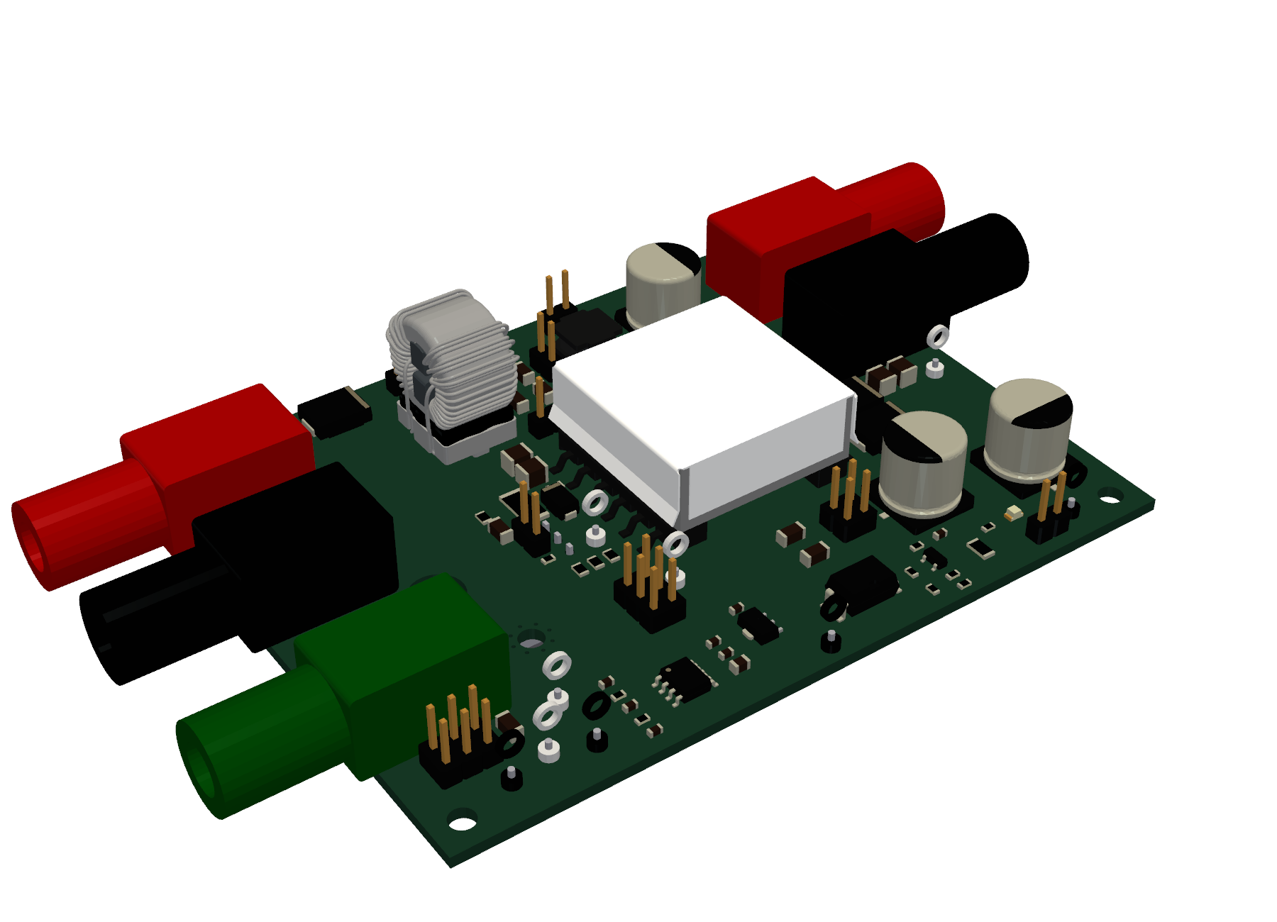
EMC demonstration flyback: a 24 V to 12 V / 1 A isolated flyback for EMC lectures, with jumper "knobs" that switch filters, gate resistance, snubber, and heatsink potential. KiCad project, LTspice simulations, 39-page design report, and fabrication files.
Design examples, bug reports, and improvements to the skill are welcome. See CONTRIBUTING.md.
This work is licensed under the Creative Commons Attribution 4.0 International License (CC BY 4.0). You may share and adapt it, including for commercial use, as long as you give credit, link to the license, and indicate if you made changes. See LICENSE for the full text.
Suggested credit: "power-pcb-design skill by Chengmin Li, Xiao Yang, https://github.com/ChengminLi/AI-PCB-layout, licensed under CC BY 4.0."
| Qty | Value | Footprint | References |
|---|---|---|---|
| 4 | 10k | Resistor_SMD:R_0603_1608Metric | R1, R8, R16, R19 |
| 4 | M3 | MountingHole:MountingHole_3.2mm_M3 | MH1, MH2, MH3, MH4 |
| 3 | 100n | Capacitor_SMD:C_0603_1608Metric | C7, C9, C11 |
| 3 | 10n 1kV | Capacitor_SMD:C_1206_3216Metric | C2, C3, C24 |
| 3 | 1k | Resistor_SMD:R_0603_1608Metric | R3, R17, R18 |
| 3 | 4.7k 1W | Resistor_SMD:R_2512_6332Metric | R9, R10, R20 |
| 3 | SS510C | Diode_SMD:D_SMC | D1, D3, D7 |
| 2 | 1n 2kV | Capacitor_SMD:C_1206_3216Metric | C14, C23 |
| 2 | 22u 25V | Capacitor_SMD:C_1210_3225Metric | C20, C21 |
| 2 | 4.7u 50V | Capacitor_SMD:C_1210_3225Metric | C5, C6 |
| 2 | 470u 25V | Capacitor_SMD:CP_Elec_10x10 | C18, C19 |
| 2 | PGND | TestPoint:TestPoint_Keystone_5000-5004_Miniature | PGND1, PGND2 |
| 1 | 0.15R 2512 | Resistor_SMD:R_2512_6332Metric | R4 |
| 1 | 100R | Resistor_SMD:R_0805_2012Metric | R7 |
| 1 | 100p 2kV | Capacitor_SMD:C_1206_3216Metric | C17 |
| 1 | 100p 2kV C0G | Capacitor_SMD:C_1206_3216Metric | C16 |
| 1 | 100u 50V | Capacitor_SMD:CP_Elec_10x10 | C4 |
| 1 | 10R | Resistor_SMD:R_1206_3216Metric | R12 |
| 1 | 10u 25V | Capacitor_SMD:C_0805_2012Metric | C8 |
| 1 | 10uH 3.3A | Inductor_SMD:L_Bourns-SRN8040_8x8.15mm | L2 |
| 1 | 1k 1206 | Resistor_SMD:R_1206_3216Metric | R13 |
| 1 | 1n | Capacitor_SMD:C_0603_1608Metric | C12 |
| 1 | 1n C0G | Capacitor_SMD:C_0603_1608Metric | C10 |
| 1 | 1u 50V | Capacitor_SMD:C_1206_3216Metric | C1 |
| 1 | 2.2mH WE-CMB | EMC_Demo:L_CommonMode_Wuerth_WE-CMB-S_744822222 | L1 |
| 1 | 220p | Capacitor_SMD:C_0603_1608Metric | C13 |
| 1 | 22R | Resistor_SMD:R_0805_2012Metric | R6 |
| 1 | 22n 100V | Capacitor_SMD:C_0805_2012Metric | C15 |
| 1 | 2A/30V PTC | Fuse:Fuse_1812_4532Metric | F1 |
| 1 | 39k | Resistor_SMD:R_0603_1608Metric | R15 |
| 1 | 4.7R | Resistor_SMD:R_0805_2012Metric | R5 |
| 1 | 4.7k | Resistor_SMD:R_0603_1608Metric | R14 |
| 1 | 47R | Resistor_SMD:R_0805_2012Metric | R11 |
| 1 | 47n | Capacitor_SMD:C_0603_1608Metric | C22 |
| 1 | 5.6k | Resistor_SMD:R_0603_1608Metric | R2 |
| 1 | 750311591 | EMC_Demo:Wurth_750311591_EFD25 | T1 |
| 1 | CHASSIS | TestPoint:TestPoint_Keystone_5000-5004_Miniature | CHAS |
| 1 | CHASSIS | EMC_Demo:Jack_4mm_RA_Cliff_FCR7350 | J5 |
| 1 | CM bypass + | Connector_PinHeader_2.54mm:PinHeader_1x02_P2.54mm_Vertical | CM1 |
| 1 | CM bypass - | Connector_PinHeader_2.54mm:PinHeader_1x02_P2.54mm_Vertical | CM2 |
| 1 | CSRAW | TestPoint:TestPoint_Keystone_5000-5004_Miniature | CS |
| 1 | Case select | Connector_PinHeader_2.54mm:PinHeader_2x03_P2.54mm_Vertical | CASE |
| 1 | Case_UChannel_revD | EMC_Demo:Case_UChannel_revD | MECH1 |
| 1 | Cover_PMMA_revD | EMC_Demo:Cover_PMMA_revD | MECH2 |
| 1 | DM bypass | Connector_PinHeader_2.54mm:PinHeader_1x02_P2.54mm_Vertical | DM |
| 1 | ES2D | Diode_SMD:D_SMA | D2 |
| 1 | GATE | TestPoint:TestPoint_Keystone_5000-5004_Miniature | GATE |
| 1 | GREEN | LED_SMD:LED_0805_2012Metric | D6 |
| 1 | HS | TestPoint:TestPoint_Keystone_5000-5004_Miniature | HS |
| 1 | IRF520NPBF | EMC_Demo:TO-220-3_BottomMount_CaseHeatsink | Q1 |
| 1 | L78L12ACUTR | Package_TO_SOT_SMD:SOT-89-3 | U2 |
| 1 | LTV-817S | Package_DIP:SMDIP-4_W9.53mm | U4 |
| 1 | M3 CASE | MountingHole:MountingHole_3.2mm_M3_Pad_Via | MH5 |
| 1 | Pri-sec Y-cap | Connector_PinHeader_2.54mm:PinHeader_2x02_P2.54mm_Vertical | YPS |
| 1 | RC snubber on | Connector_PinHeader_2.54mm:PinHeader_1x02_P2.54mm_Vertical | SNUB |
| 1 | RED | LED_SMD:LED_0805_2012Metric | D5 |
| 1 | Rg select | Connector_PinHeader_2.54mm:PinHeader_2x03_P2.54mm_Vertical | RG |
| 1 | SGND | TestPoint:TestPoint_Keystone_5000-5004_Miniature | SGND |
| 1 | SGND to chassis | Connector_PinHeader_2.54mm:PinHeader_1x02_P2.54mm_Vertical | SGCH |
| 1 | SW | TestPoint:TestPoint_Keystone_5000-5004_Miniature | DRAIN |
| 1 | TL431AIDBZR | Package_TO_SOT_SMD:SOT-23 | U3 |
| 1 | UC3845B | Package_SO:SOIC-8_3.9x4.9mm_P1.27mm | U1 |
| 1 | VBUS | TestPoint:TestPoint_Keystone_5000-5004_Miniature | VBUS |
| 1 | VIN+ 24V | EMC_Demo:Jack_4mm_RA_Cliff_FCR7350 | J1 |
| 1 | VIN- 0V | EMC_Demo:Jack_4mm_RA_Cliff_FCR7350 | J2 |
| 1 | VOUT | TestPoint:TestPoint_Keystone_5000-5004_Miniature | VOUT |
| 1 | VOUT +12V | EMC_Demo:Jack_4mm_RA_Cliff_FCR7350 | J3 |
| 1 | VOUT 0V | EMC_Demo:Jack_4mm_RA_Cliff_FCR7350 | J4 |
| 1 | Y-caps to chassis | Connector_PinHeader_2.54mm:PinHeader_1x02_P2.54mm_Vertical | YCAP |
nunosousa/SCART-switcher
An old school SCART switcher. Its main purpose will be to automaticaly detect and switch the video output to the active input video source.


Majklzbastlirny/NixieClock
ESP-IDF firmware for a 6-tube multiplexed ESP32 nixie clock (WiFi/SNTP, Home Assistant, web UI, alarm, temperatures)

atomicra1n/wifi-geiger-counter
A DIY Geiger counter PCB which can detect ionizing radiation and log readings over Wi-Fi. Built with an ESP32, and a HV multiplier circuit that steps up 3.7V to 400V for the GM tube.


JimKueneman/TurnoutBoss
This repository contains all the design files, manuals, firmware, production information for the LCC TurnoutBoss Node

JohnanLuca02/BYTE_Electronics
Repository for everything concerning the electronics (PCB, Electrical schemes, BOM, ...) of the robot dog project of the AiTeam called BYTE.
It measures 100 × 76 mm and has 2 copper layers, 1.6 mm thick.
90 parts, built around the UC3845B, L78L12ACUTR-CN, LTV-817S and TL431AIDBZR. The full list of its parts is on this page, with links to each part's symbol and footprint where PCBKit's library has them.
From the ChengminLi/AI-PCB-layout repository on GitHub, at the commit this page was made from: the board is examples/emc-flyback-demo/design/emc_flyback.kicad_pcb and its schematic examples/emc-flyback-demo/design/emc_flyback.kicad_sch. PCBKit opens the board in the browser, with nothing to install.
Its repository publishes it under the CC-BY-4.0 licence: you may reuse it on that licence's terms (keep the author's notice, and for a copyleft licence share your changes alike).