2 layers30 × 61.3 mm

 Cheetah26/keyboard
Fully custom split keyboard
Keyboard is an open-source printed circuit board by Cheetah26, from the Cheetah26/keyboard repository on GitHub. It is a 2-layer board of 141.8 × 81.6 mm with 47 parts on 44 nets, routed with 600 tracks and 0 vias.
Its parts include 20 diodes, 20 switches, 1 IC and 1 connector. It belongs with the keyboards and input boards and the AVR (ATmega, ATtiny) boards of this library.
My fully custom split keyboard
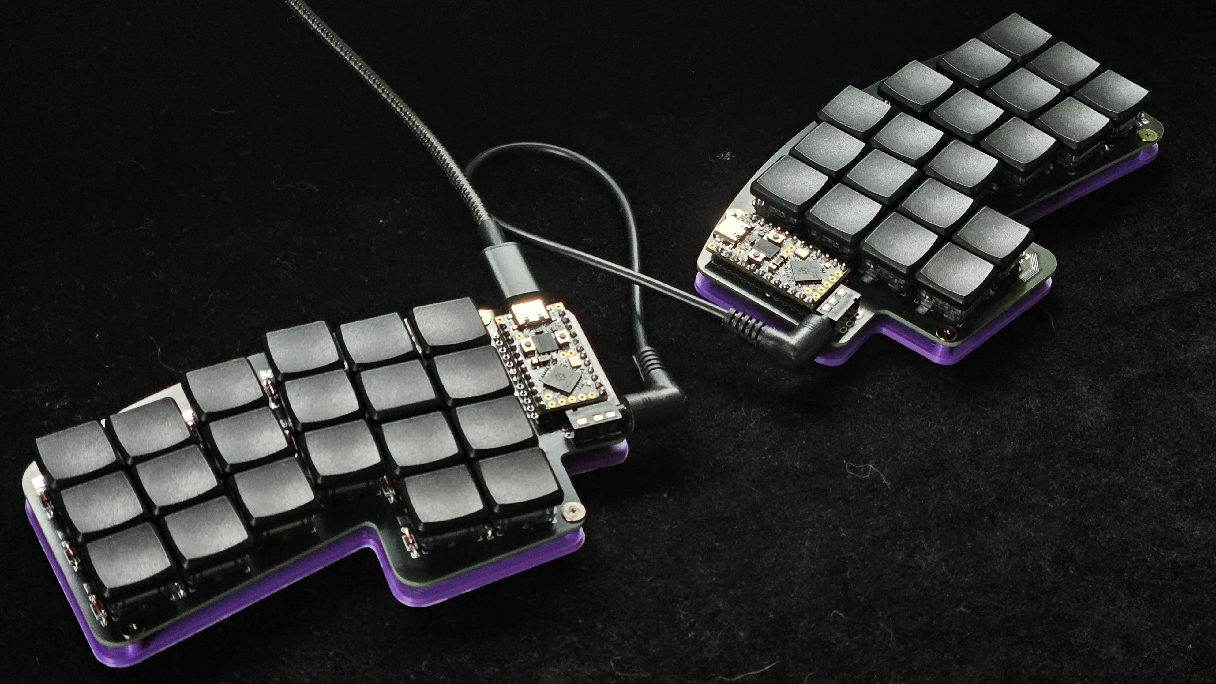
After years of wanting an ergonomic split keyboard but never seeing one that perfectly matched what I imagined in my mind, I decided to design and build my own!
I started completely from scratch by putting my hand on a sheet of paper and just seeing where my fingers liked to be. From there I made a layout based on where keys could actually go, and iterated until things really felt right.
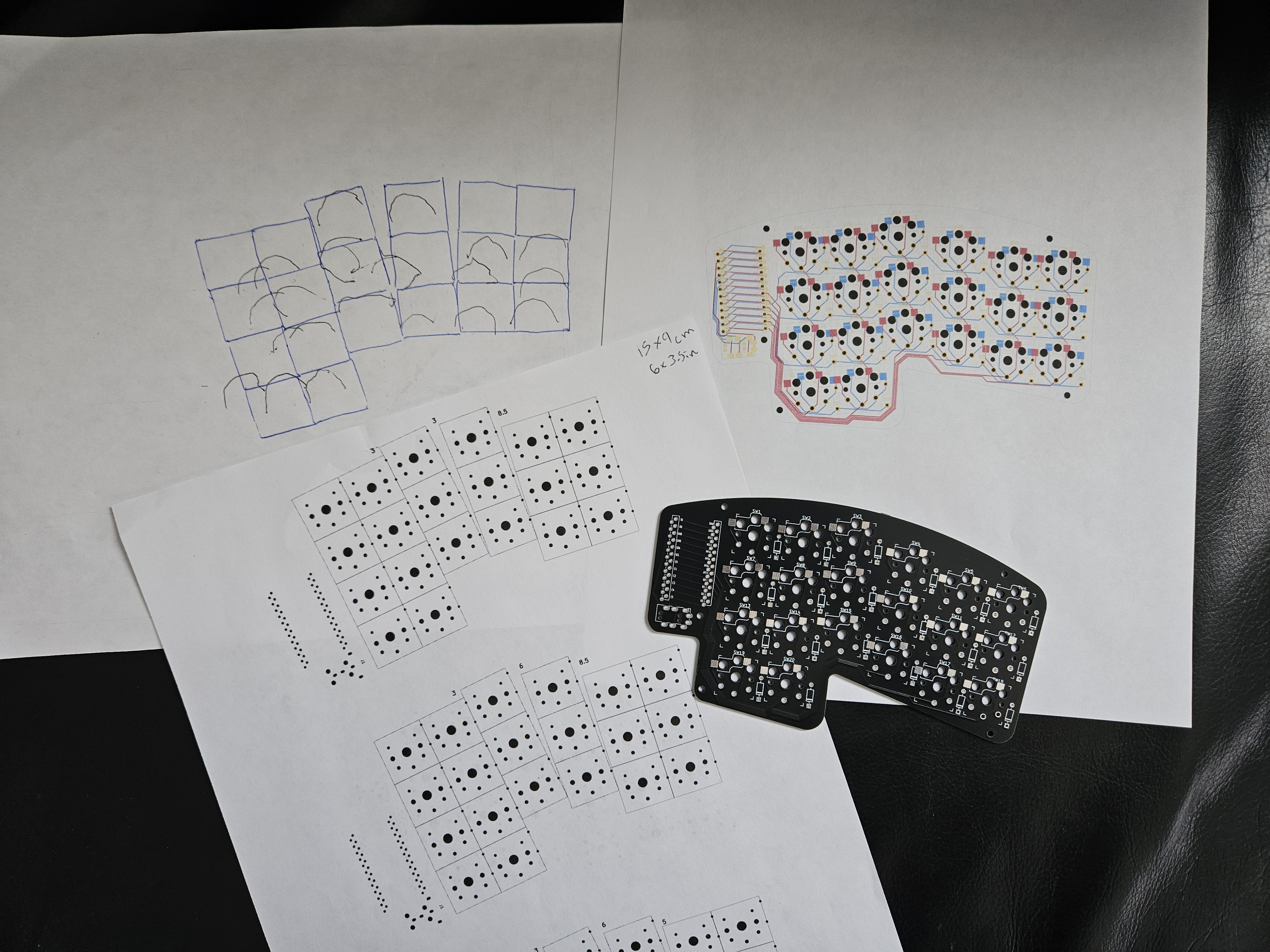
I laid out the PCB according to this design, ordered all the parts, and anxiously waited to find out what I messed up. Since this was my first time designing a PCB, fist time programming a microcontroller, and first big soldering project, I 100% expected something to go wrong. To my surprise, the only issue was that I forgot to account for the size of the jack connecting each half. After a little sanding, everything went together perfectly and now I couldn't be happier with it.
| Qty | Value | Footprint | References |
|---|---|---|---|
| 20 | 1N4148 | keyboard:Diode | D1, D2, D3, D4, D5, D10, D11, D12, D13, D14, D15, D16, D17, D18, D19, D20 +4 |
| 20 | Choc | keyboard:Kailh_socket_PG1350_optional_reversible_outline | SW1, SW2, SW3, SW4, SW5, SW10, SW11, SW12, SW13, SW14, SW15, SW16, SW17, SW18, SW19, SW20 +4 |
| 1 | ProMicro | keyboard:ProMicro | U1 |
| 1 | TRRS | keyboard:PJ320-A_TRRS | J1 |
The 42 most common of 47 parts.
It measures 141.8 × 81.6 mm and has 2 copper layers, 1.6 mm thick.
47 parts. The full list of its parts is on this page, with links to each part's symbol and footprint where PCBKit's library has them.
From the Cheetah26/keyboard repository on GitHub, at the commit this page was made from: the board is pcb/keyboard.kicad_pcb and its schematic pcb/keyboard.kicad_sch. PCBKit opens the board in the browser, with nothing to install.
Its repository states no licence, so its author keeps all rights: ask Cheetah26 before reusing the design.


VoronDesign/Voron-Hardware
Cool Hardware designed by the Voron Design group

hackclub/OnBoard
💡 Join 1,000 teenagers and make your first PCB with a $100 grant!


FrameworkComputer/InputModules
Reference designs and documentation for the Input Module system in the Framework Laptop 16