
2 layers115.6 × 106.7 mm
ErgoSNM v3 left
siderakb/ergo-snm-keyboard
ErgoSNM is a split ergonomic keyboard integrated with trackball, wireless is in beta
90 parts172CERN-OHL-P-2.0
 Chameleon-Electronics/dev-board1
nRF52840 development board
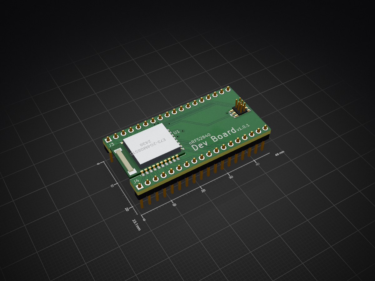
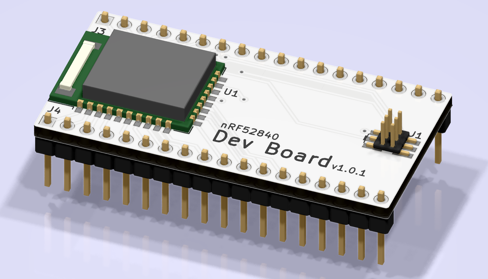
Dev board is an open-source printed circuit board by Chameleon-Electronics, from the Chameleon-Electronics/dev-board repository on GitHub, published under the GPL-3.0 licence. It is a 2-layer board of 46 × 23.1 mm with 4 parts on 36 nets, routed with 163 tracks and 20 vias.
It is built around the E73-2G4M08S1C. Its parts include 3 connectors and 1 IC. It belongs with the microcontroller boards boards of this library.

The board we use to prototype our ideas, this is where it all starts.
Open an issue or if you're feeling excited submit a pull request! We are always looking for new features and improvements.
You can use this at your will provided that you mention us properly by including a link to this page.
| Qty | Value | Footprint | References |
|---|---|---|---|
| 2 | Conn_01x18_Male | Connector_PinHeader_2.54mm:PinHeader_1x18_P2.54mm_Vertical | J3, J4 |
| 1 | Conn_Chameleon_SWD | IoT_Home:Chameleon_SWD_Header | J1 |
| 1 | E73-2G4M08S1C | IoT_Home:E73-2G4M08S1C | U1 |
It measures 46 × 23.1 mm and has 2 copper layers, 1.6 mm thick.
4 parts, built around the E73-2G4M08S1C. The full list of its parts is on this page, with links to each part's symbol and footprint where PCBKit's library has them.
From the Chameleon-Electronics/dev-board repository on GitHub, at the commit this page was made from: the board is hardware/dev-board.kicad_pcb. PCBKit opens the board in the browser, with nothing to install.
Its repository publishes it under the GPL-3.0 licence: you may reuse it on that licence's terms (keep the author's notice, and for a copyleft licence share your changes alike).
siderakb/ergo-snm-keyboard
ErgoSNM is a split ergonomic keyboard integrated with trackball, wireless is in beta

weteor/LuttUnLutt
Lütt Un Lütt is a small 3x5+2 split ortho keyboard with encoder


siderakb/calcite
60/52 keys Kailh Choc V1 low profile switches ortho keyboard

neuman/gripster
thumbdeck — wireless split thumb keyboard (nRF52840 + ZMK, BLE split, i8+-inspired). Layout converged & graded PASS.

ericrlau/SP56
Bluetooth low engery keyboard. Layout based on Sofle keyboard with some modifications. NRF52840 powered. Designed around Kaihl Choc switches and spacing.

Rogger/schneggi-sensor
A low-power ZigBee sensor integrated with HomeAssistant for monitoring temperature, humidity, and CO2.