
2 layers144.1 × 108.1 mm
 cellularmitosis/scanner1
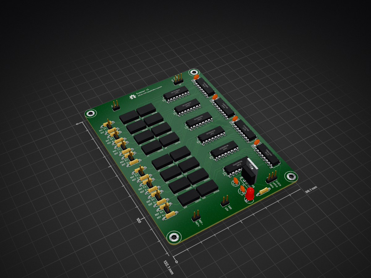
A relay board for scanning voltage references.
Scanner is an open-source printed circuit board by cellularmitosis, from the cellularmitosis/scanner repository on GitHub, published under the MIT licence. It is a 2-layer board of 99.1 × 132.1 mm with 69 parts on 109 nets, routed with 921 tracks and 0 vias.
It is built around the ULN2003A and 74HC595. Its parts include 17 resistors, 16 switches, 13 connectors, 11 ICs and 6 capacitors. It belongs with the home automation and IoT boards of this library.
This ia a relay board for scanning voltage references.
| Qty | Value | Footprint | References |
|---|---|---|---|
| 16 | 4k7 | PL_R_AXIAL_0W25_059A | R2, R3, R4, R5, R6, R7, R8, R9, R10, R11, R12, R13, R14, R15, R16, R17 |
| 16 | V23026 | PL_V23026 | K1, K2, K3, K4, K5, K6, K7, K8, K9, K10, K11, K12, K13, K14, K15, K16 |
| 11 | CONN_2X1 | PL_SIL-2-MCHN | P1, P3, P4, P5, P6, P7, P8, P9, P10, P11, P13 |
| 6 | ULN2003A | PL_DIP16 | IC5, IC6, IC7, IC8, IC9, IC10 |
| 4 | 0.1uF | PL_ANYSSCAP_SMALL_2_059B_0805 | C1, C2, C3, C4 |
| 4 | 74HC595 | PL_DIP16 | IC1, IC2, IC3, IC4 |
| 4 | Val** | PL_hole_M3 | H***, H***, H***, H*** |
| 2 | CONN_3X1 | PL_SIL-3-MCHN | P2, P12 |
| 1 | 10uF | PL_ELCAP_10_20_V_059A | C5 |
| 1 | 1uF | PL_ELCAP_10_20_V_059A | C6 |
| 1 | 220 | PL_R_AXIAL_0W25_059A | R1 |
| 1 | 7805 | PL_TO-220_V_069A | U1 |
| 1 | LED | PL_LED_5MM | D1 |
| 1 | OSHW-logo_silkscreen-front_5mm | OSHW-logo_silkscreen-front_5mm | G*** |
It measures 99.1 × 132.1 mm and has 2 copper layers, 1.6 mm thick.
69 parts, built around the ULN2003A and 74HC595. The full list of its parts is on this page, with links to each part's symbol and footprint where PCBKit's library has them.
From the cellularmitosis/scanner repository on GitHub, at the commit this page was made from: the board is scanner.kicad_pcb. PCBKit opens the board in the browser, with nothing to install.
Its repository publishes it under the MIT licence: you may reuse it on that licence's terms (keep the author's notice, and for a copyleft licence share your changes alike).

cellularmitosis/gate-timer
A beam-interrupt timer with a large 7-segment display.


ra0sms/universal_control_console
Control console for any types of antenna's switches

