4 layers55 × 72 mm
DB9 Differential Signal Selector
nanographs/Open-Beam-Interface
Just what you need to control the beam and get an image.
18 parts371

 BuildersInc/EthernetLatencyTestplatform1
Used to measure the time difference within the Ethernet communication between two uC's
ZeitMessung is an open-source printed circuit board by BuildersInc, from the BuildersInc/EthernetLatencyTestplatform repository on GitHub, published under the MIT licence. It is a 4-layer board of 50.5 × 61.2 mm with 18 parts on 42 nets, routed with 122 tracks and 120 vias.
Its parts include 6 resistors, 3 capacitors, 3 connectors, 2 ICs and 1 diode.
Used to measure the time difference within the Ethernet communication between two uC's
Created for my Bachelor Thesis
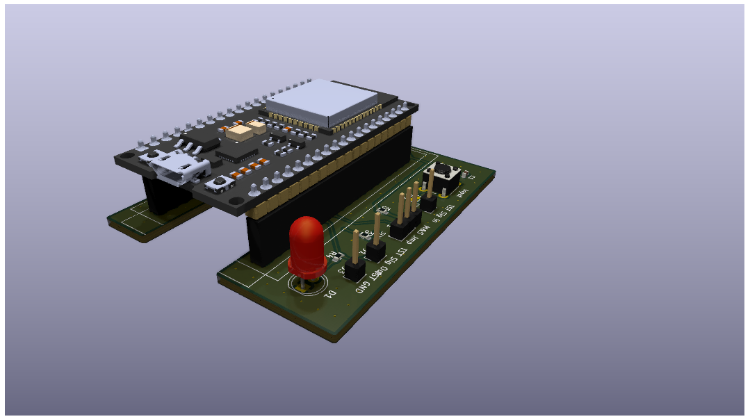
| GPIO | Function |
|---|---|
| 00 | RETCLK |
| 12 | Output detection |
| 13 | Input detection |
| 14 | Master & Slave |
| 17 | NC |
| 18 | MDC |
| 19 | TX 0 |
| 21 | TX Enable |
| 22 | TX 1 |
| 23 | MDIO |
| 25 | RX 0 |
| 26 | RX 1 |
| 27 | CRS |
| Qty | Value | Footprint | References |
|---|---|---|---|
| 5 | 4k7 | Resistor_SMD:R_0603_1608Metric | R1, R2, R3, R5, R6 |
| 3 | 100 nF | Capacitor_SMD:C_0603_1608Metric | C1, C2, C3 |
| 1 | 470 | Resistor_SMD:R_0603_1608Metric | R4 |
| 1 | Input | Button_Switch_THT:SW_PUSH_6mm | SW1 |
| 1 | LED | LED_THT:LED_D5.0mm | D1 |
| 1 | M&S Jmp | Connector_PinHeader_2.54mm:PinHeader_1x03_P2.54mm_Vertical | JP1 |
| 1 | Switch | Jumper:SolderJumper-2_P1.3mm_Open_RoundedPad1.0x1.5mm | JP2 |
| 1 | TST GND | Connector_PinHeader_2.54mm:PinHeader_1x01_P2.54mm_Vertical | J3 |
| 1 | TST Sig In | Connector_PinHeader_2.54mm:PinHeader_1x01_P2.54mm_Vertical | J2 |
| 1 | TST Sig Out | Connector_PinHeader_2.54mm:PinHeader_1x01_P2.54mm_Vertical | J1 |
| 1 | ~ | Library:ESP32-WROOM | U2 |
| 1 | ~ | Library:LAN8720 DevBoard | U1 |
It measures 50.5 × 61.2 mm and has 4 copper layers, 1.6 mm thick.
18 parts. The full list of its parts is on this page, with links to each part's symbol and footprint where PCBKit's library has them.
From the BuildersInc/EthernetLatencyTestplatform repository on GitHub, at the commit this page was made from: the board is Hardware/ZeitMessung.kicad_pcb and its schematic Hardware/ZeitMessung.kicad_sch. PCBKit opens the board in the browser, with nothing to install.
Its repository publishes it under the MIT licence: you may reuse it on that licence's terms (keep the author's notice, and for a copyleft licence share your changes alike).
nanographs/Open-Beam-Interface
Just what you need to control the beam and get an image.


khill25/Dreamdrive
Open source Retro Rom Carts and ODEs by Dreamcraft Industries

mirdej/vmix
Multichannel modular analog PAL video mixer based on the SYNKIE project


probe-rs/hive
A Raspberry PI shield for testing probe-rs against many chips & probes.