
2 layers50 × 50 mm
Gerber
buganini/Kikakuka
Kikakuka — KiCad Workspace, Panelization, Build Variants, Differ & FreeCAD PCB Bending and Assembly
10 parts81MIT

Kikakuka — KiCad Workspace, Panelization, Build Variants, Differ & FreeCAD PCB Bending and Assembly
Dcdc is an open-source printed circuit board by buganini, from the buganini/Kikakuka repository on GitHub, published under the MIT licence. It is a 4-layer board of 43.6 × 17.4 mm with 12 parts on 8 nets, routed with 25 tracks and 12 vias.
Its parts include 6 capacitors, 2 resistors, 2 connectors, 1 IC and 1 inductor. It belongs with the power boards of this library.





Kikakuka (企画課, きかくか, Planning Section) creates a few more dimensions for KiCad:
Kikakuka main program
.kkkk workspaces with relative paths and file descriptions${KIPRJMOD}-relative references.kkkk_fab file..kkkk_fab, or legacy .kikit_pnl) to KiCad files in one commandFreekiCAD (FreeCAD Addon)
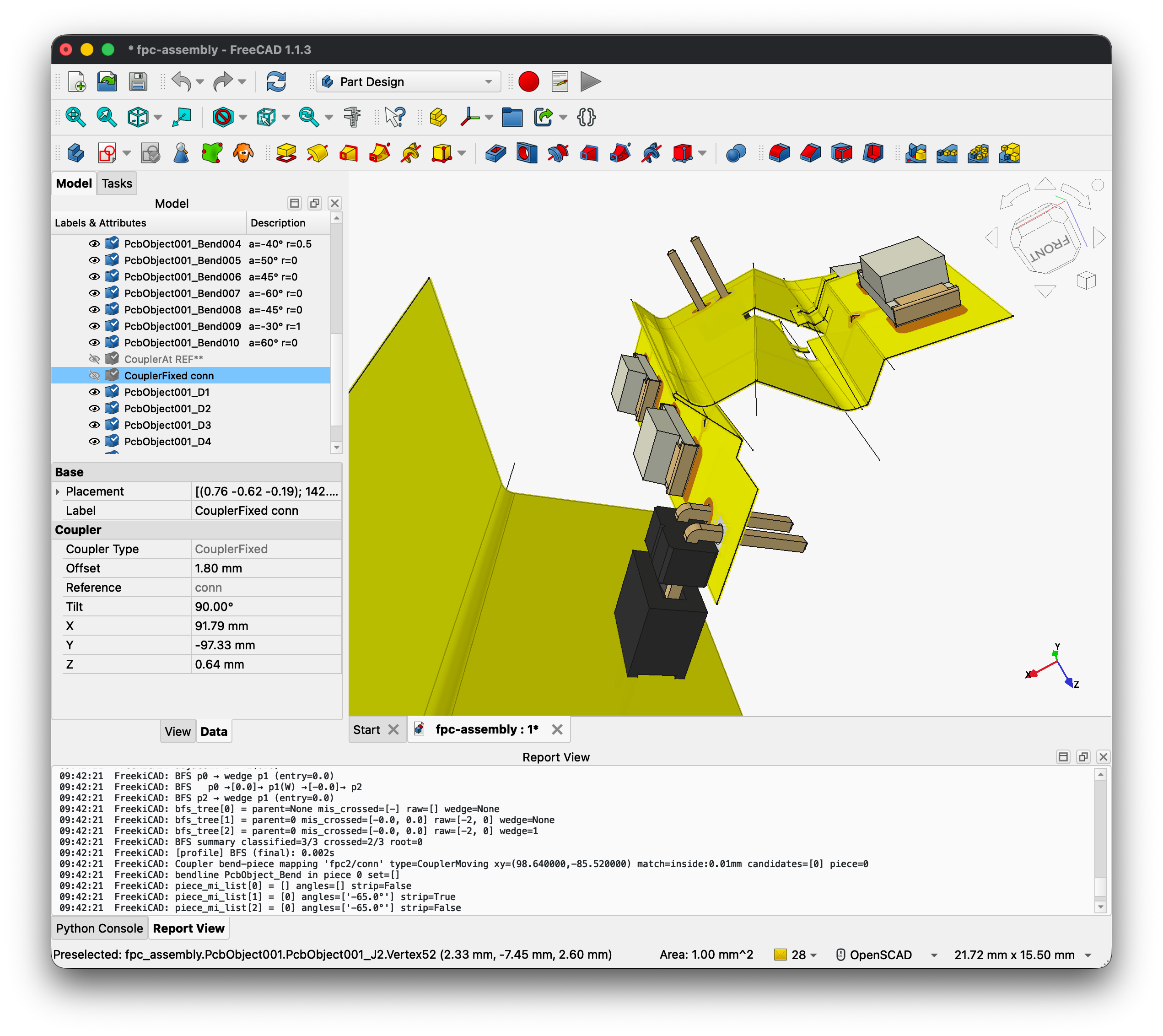
F.Stiffener and B.Stiffener user-layer areasCouplerFixed and CouplerMoving footprints or an absolute CouplerAt, with coupler plane markers for inspection.kkkk_asm).kkkk_asm) to STEP or STL in one commandKiCad Plugin/Library
Coupler footprints for Automatic coupler-based PCB alignment
Plugin actions for previewing and hiding coupler helpers in the 3D Viewer
Populate scaled placeholder 3D models for footprints without a valid model, using SizeX, SizeY, and SizeZ properties
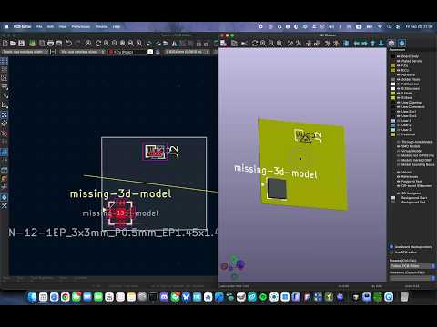
CADhoc / Instance Manager
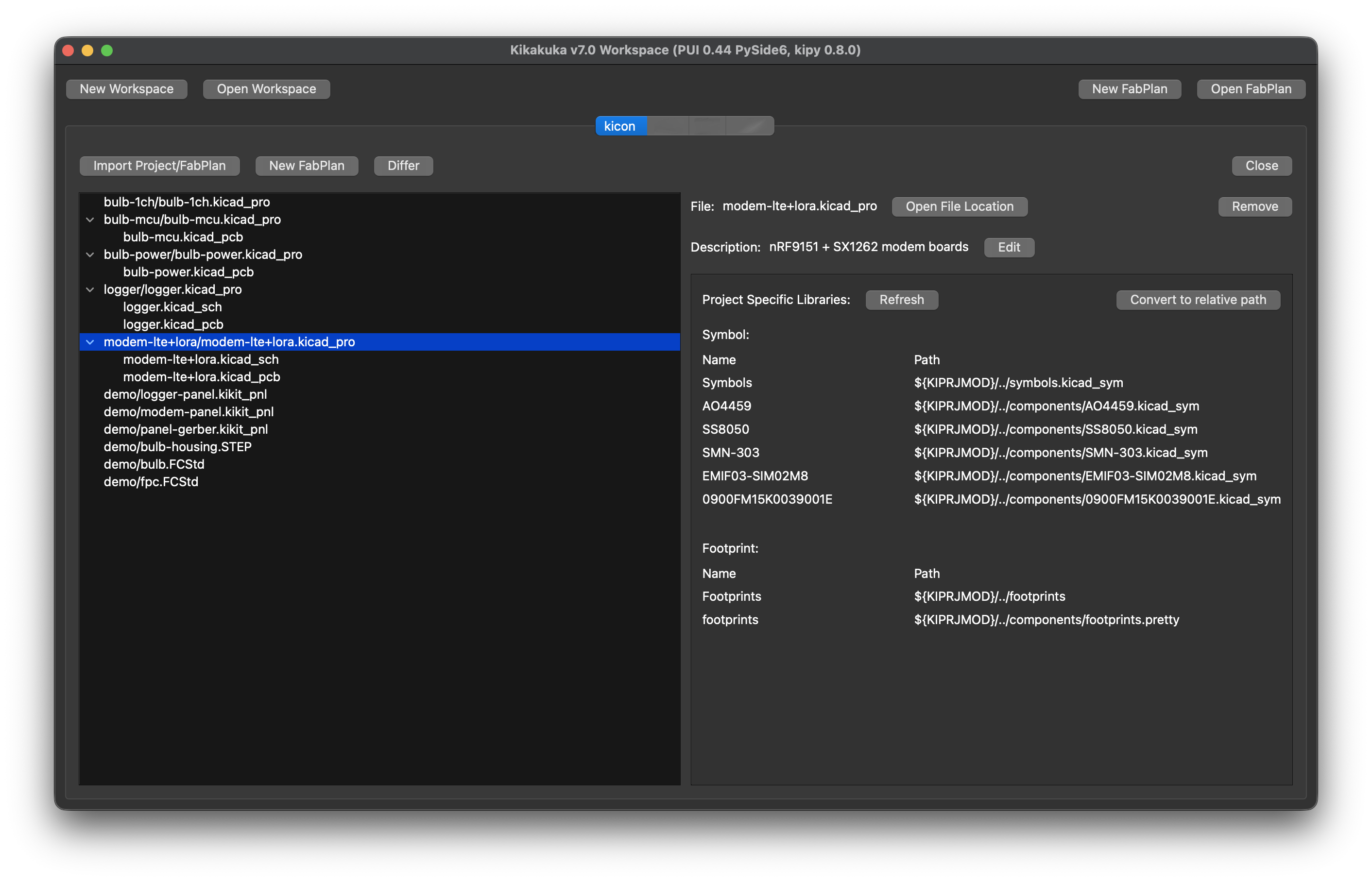
The .kkkk file saves workspace information in JSON format.
Adding or dropping a .kicad_pcb or .kicad_sch records its sibling
.kicad_pro project entry, even when that project file has not been created
yet. A virtual project row omits the .kicad_pro suffix; an existing project
file keeps it. Rows list only PCB/schematic files that currently exist.
Opening a missing project row reports the missing project instead of launching
KiCad.
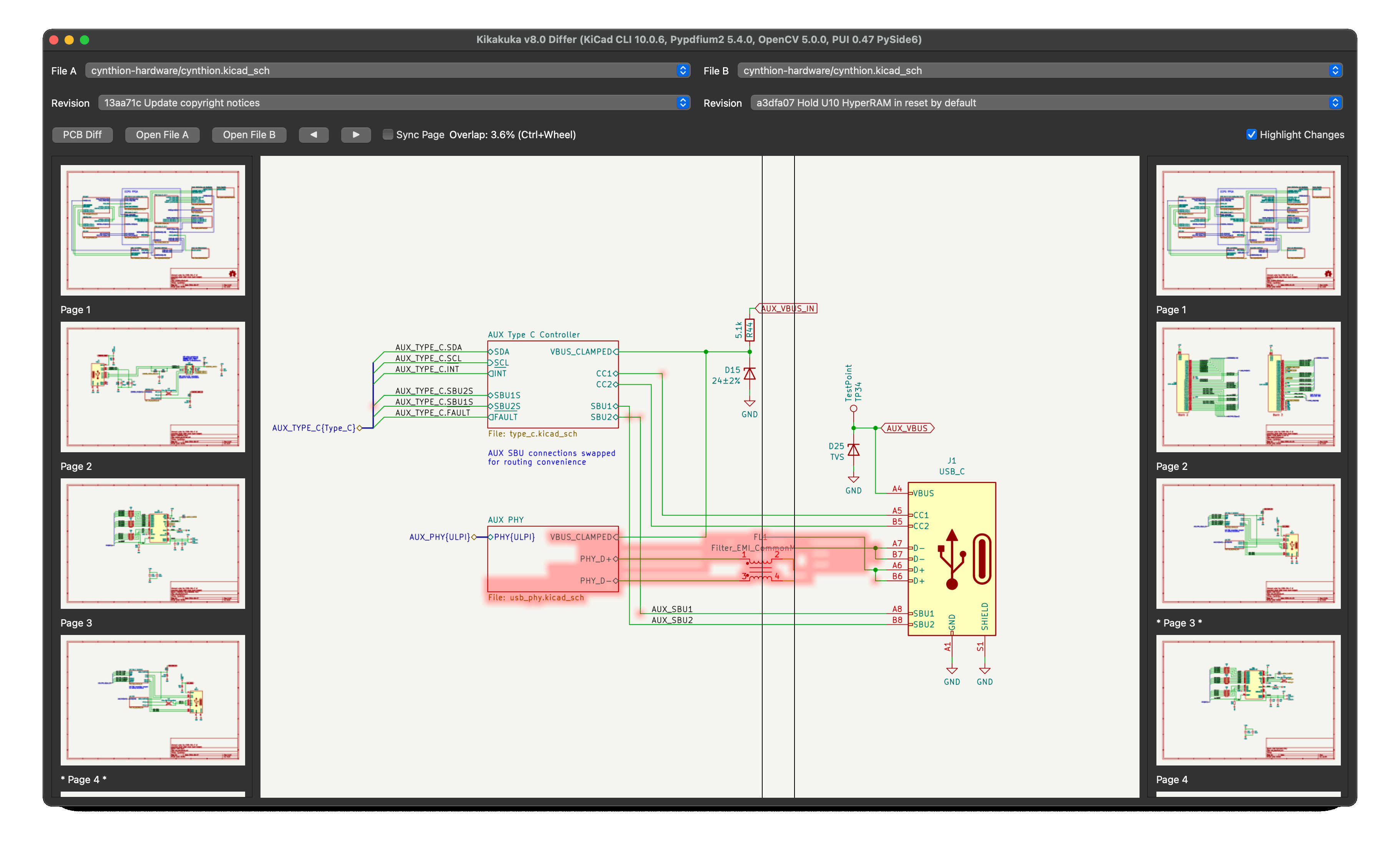
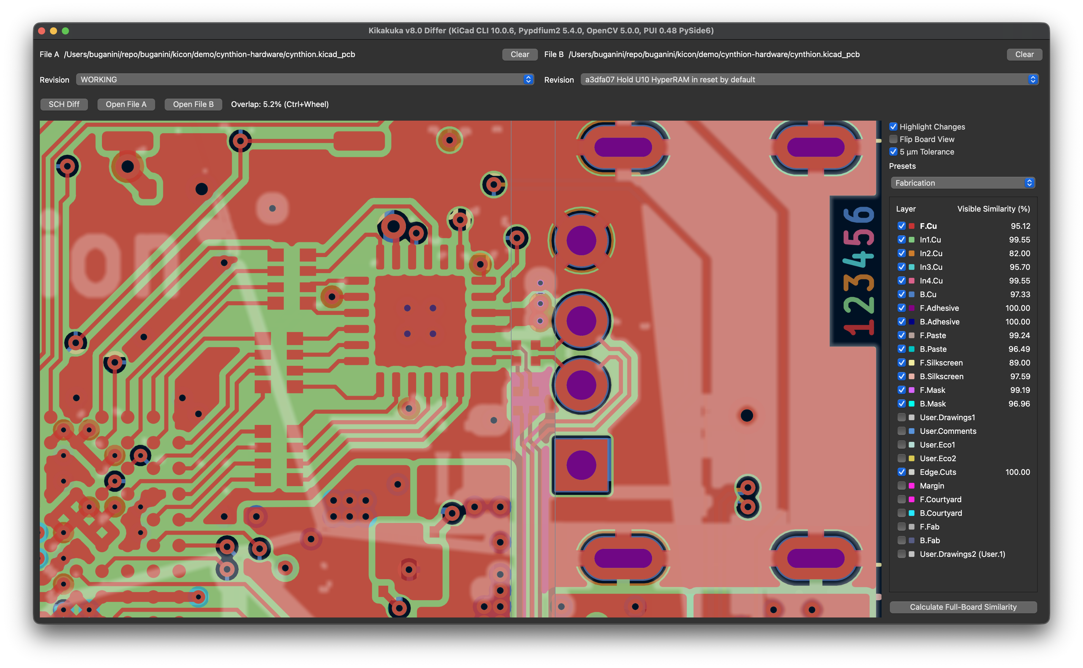
The .kkkk_fab file saves panelization and build-variants settings in JSON format, with PCB paths stored relative to the file's location. Legacy .kikit_pnl files can still be opened or added; newly saved fabrication plans use .kkkk_fab.
Example: samples/build_variant.kkkk_fab and samples/build_variant.kicad_pcb.
Set BUILDEXPR in footprints' properties. This can be done quickly with Symbol Fields Table using the current sheet only scope. Remember to sync them to PCB afterward.
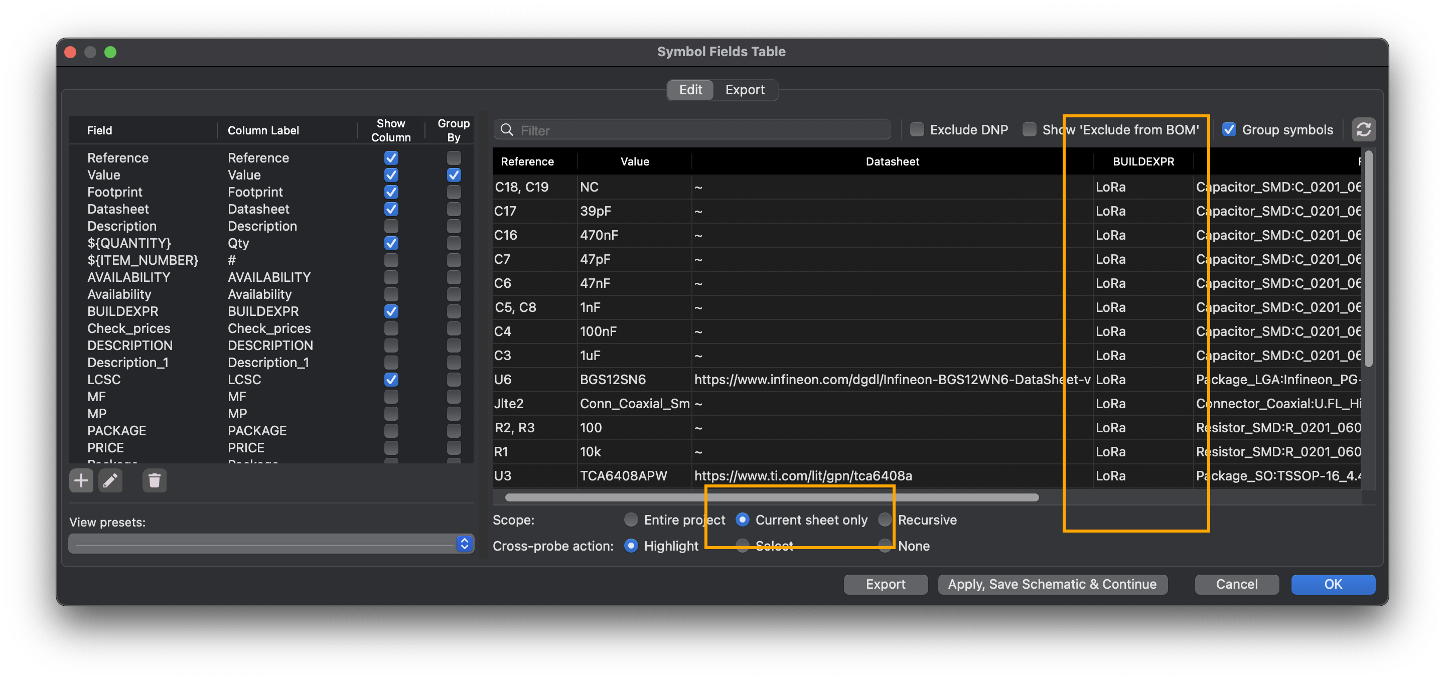
BUILDEXPR. Selected flags are interpreted as true, and vice versa.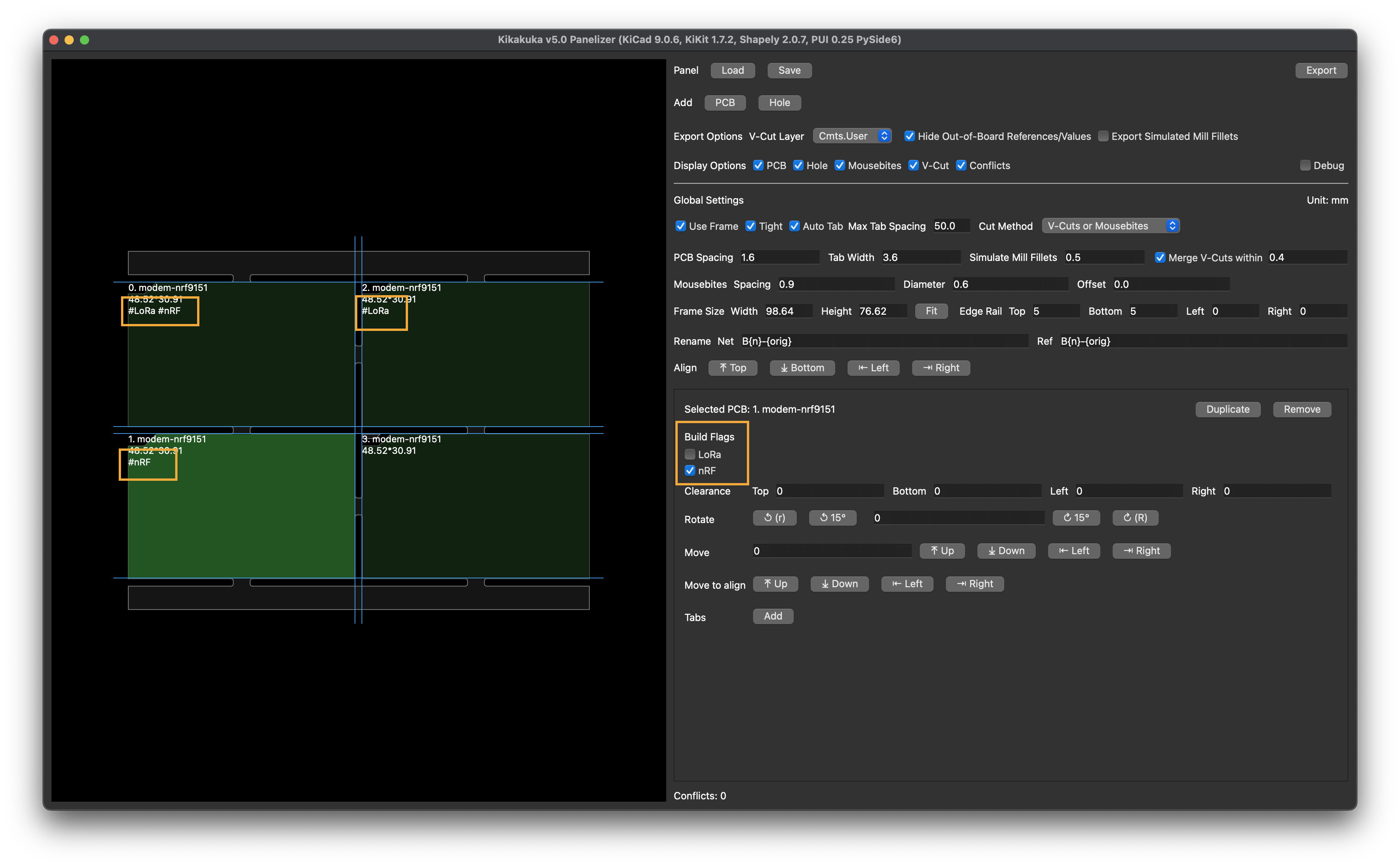
A boolean expression with operators:
~ Not& And| OrIt can be as simple as a build name as shown in the image above or an expression like (A | ~B) & C.
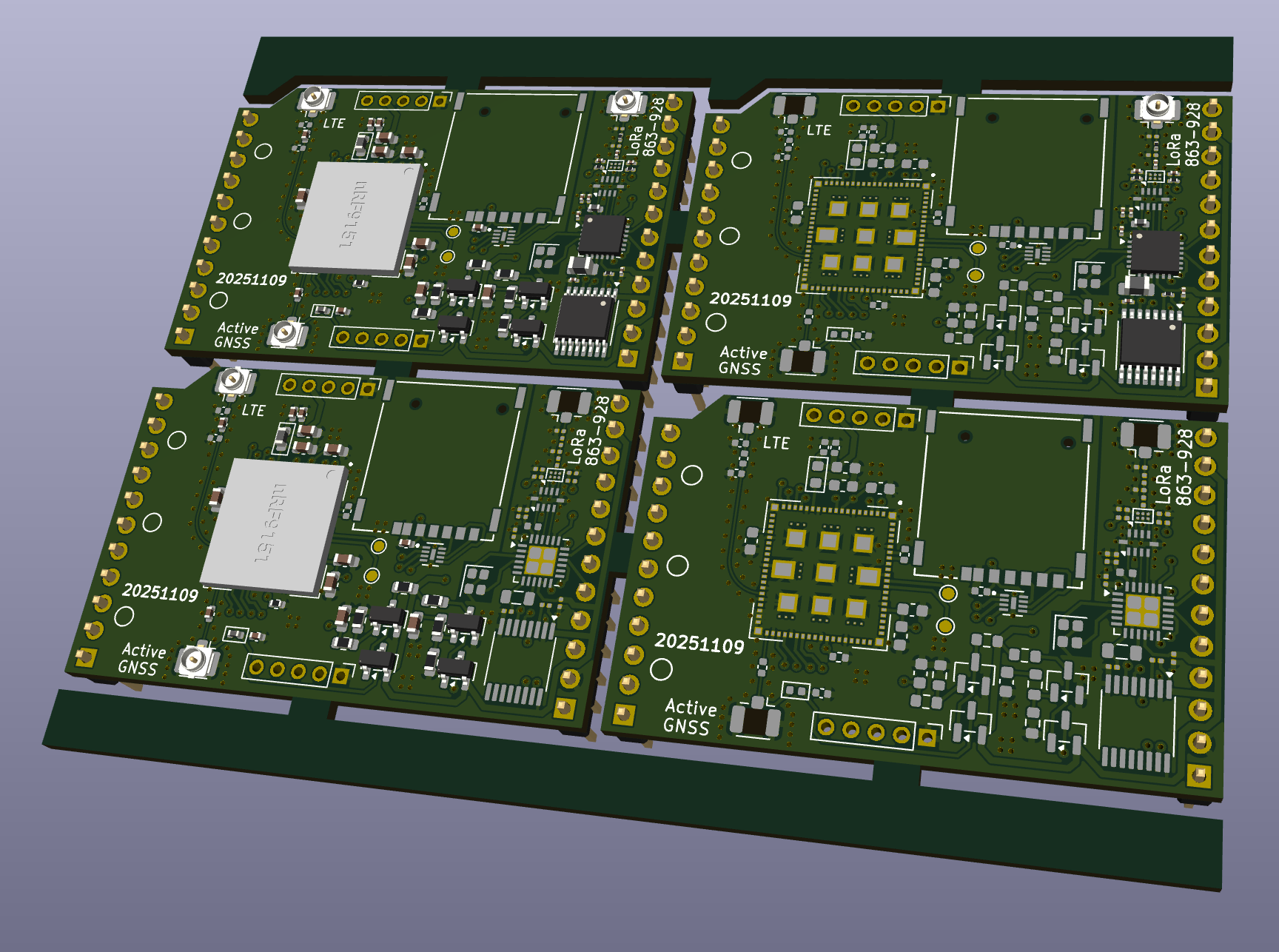
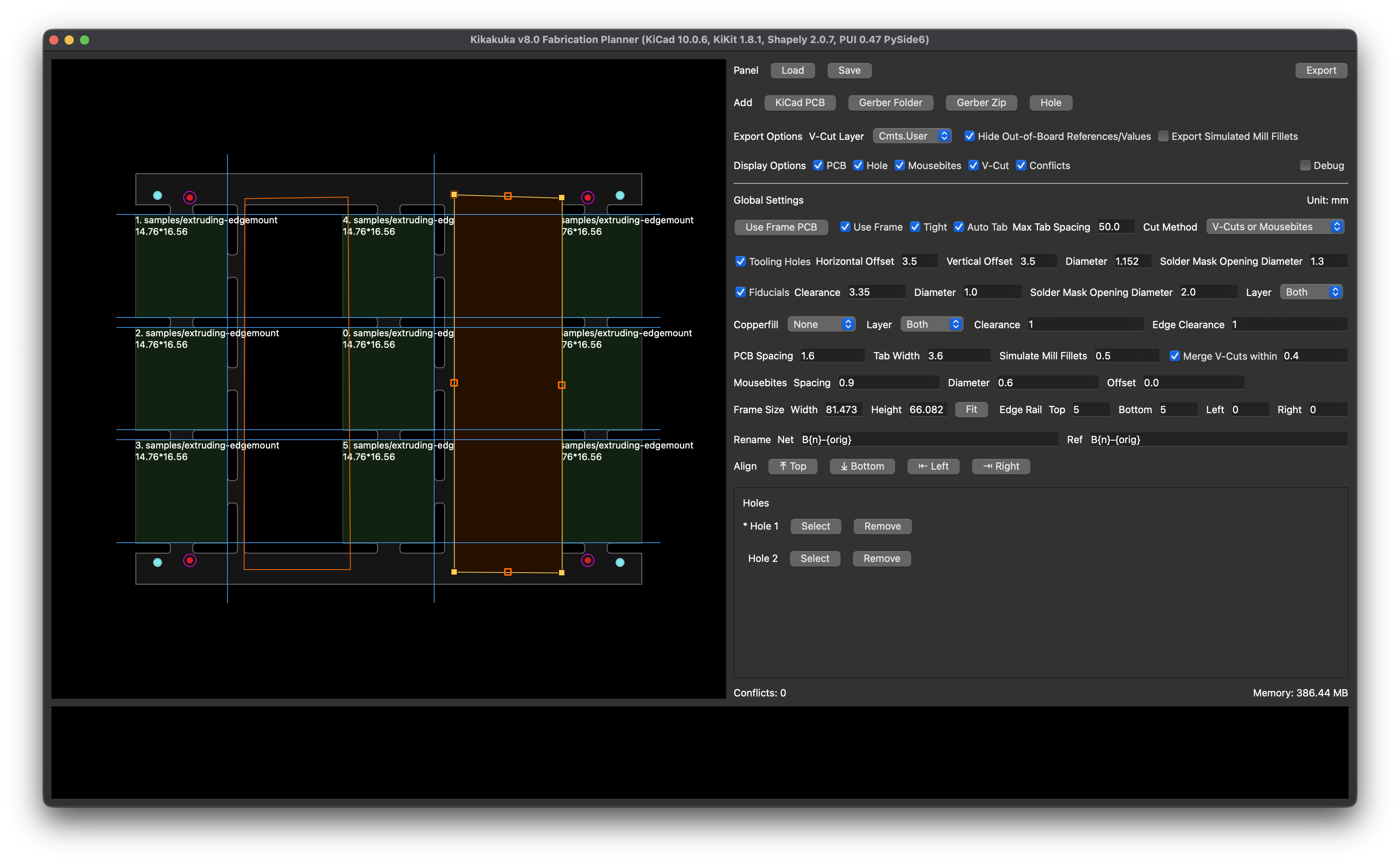
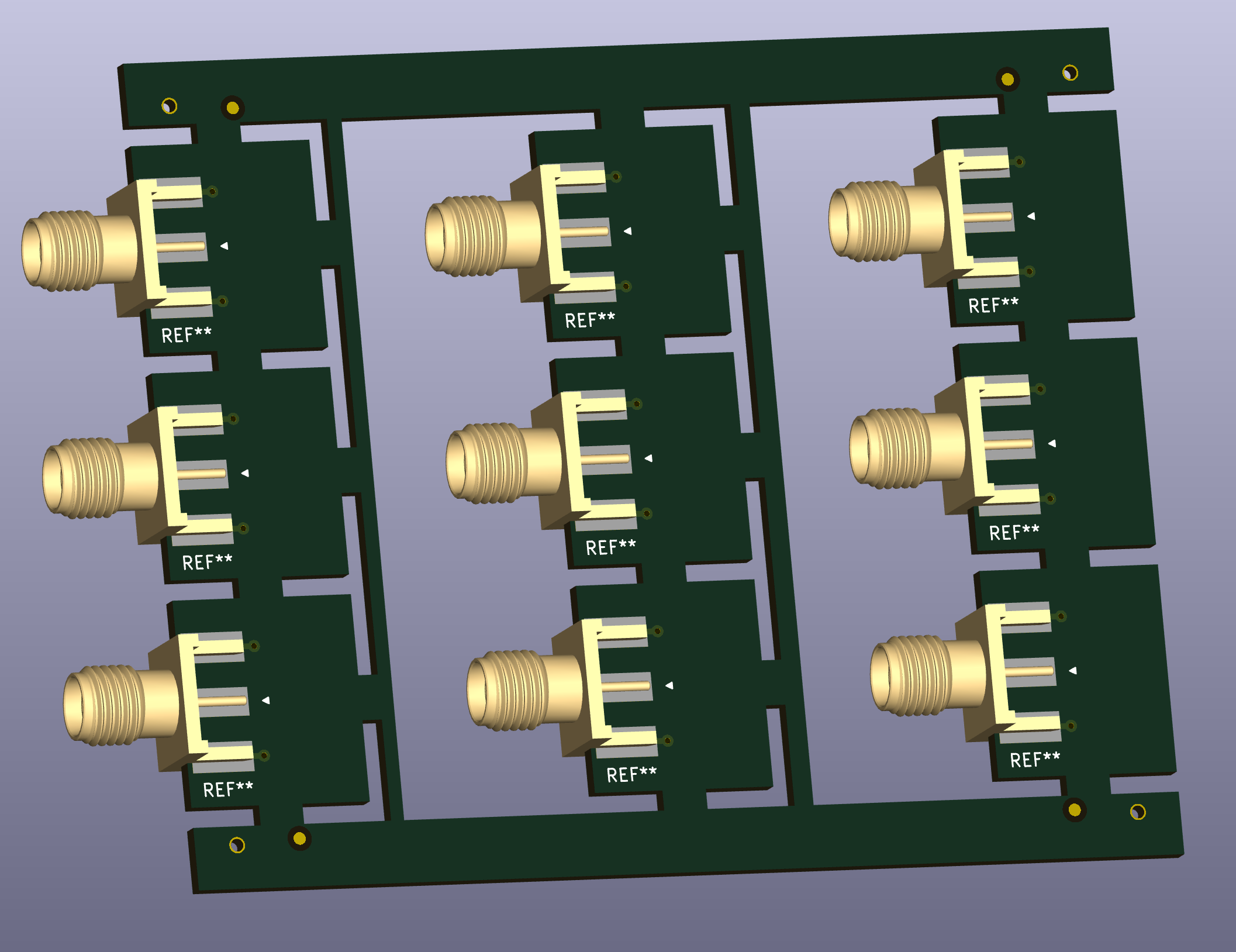
Panelization with different build variants
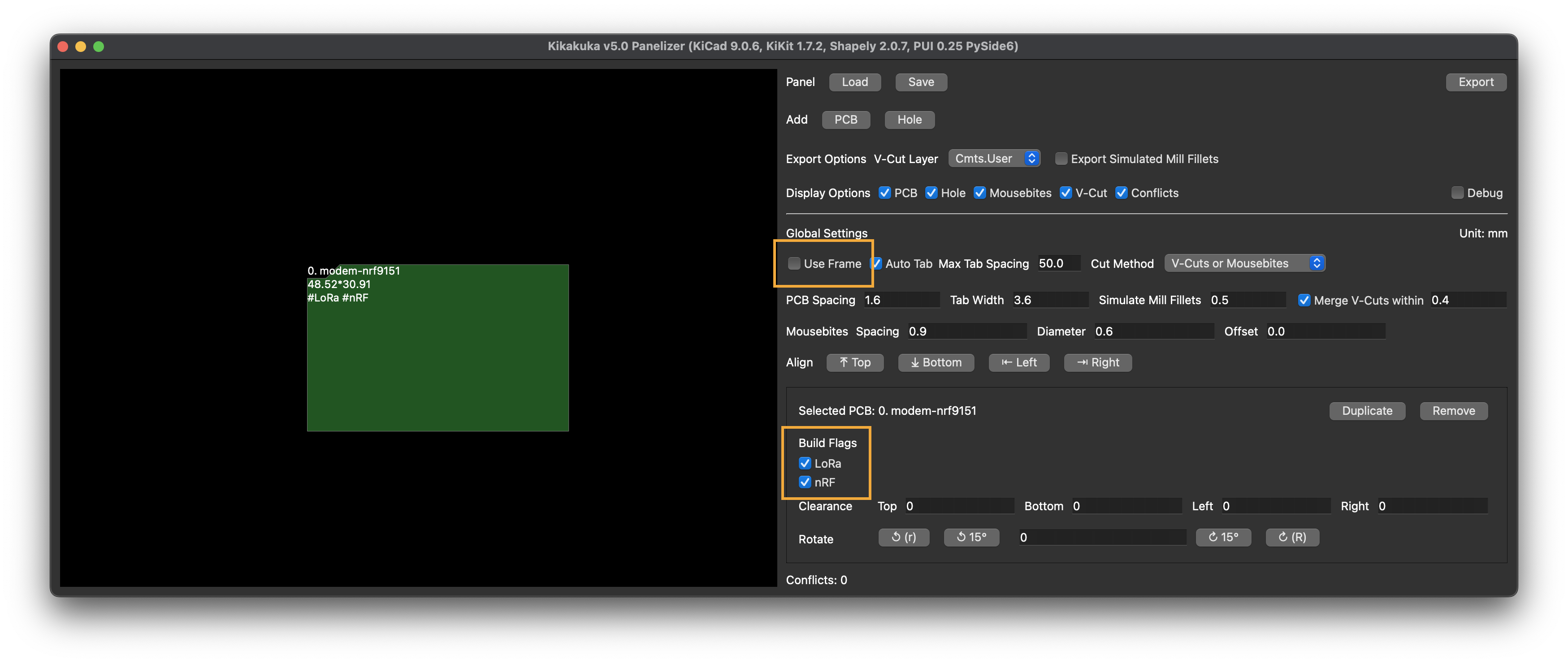
Single PCB without panelization can be done with frameless setting
Field#Flag or multiple flags like Field#FlagA#FlagB will set Field to the value where build flags contain all the flags.
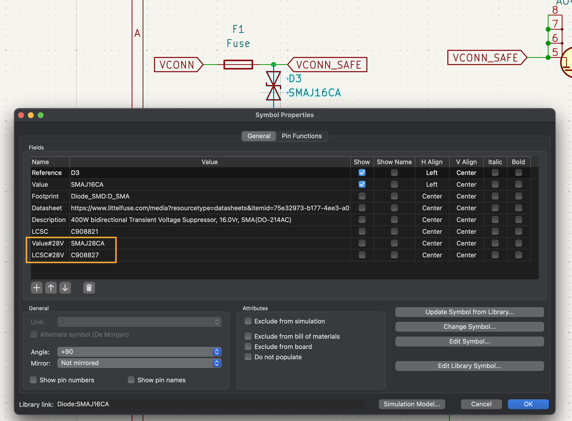
Field#Opt=A, Field#Opt=B will be displayed as dropdown options.
Requires FreeCAD 1.0 or later, KiCad 9.0 or later,
psutil>=7.2.2, kicad-python>=0.8,<0.9, and shapely>=2.0.7. FreeCAD Addon
Manager may not automatically install packages where its allowed-package list
excludes them; install them manually inside FreeCAD if necessary. Installing
FreekiCAD from Kikakuka's Integration tab installs all three Python packages.
[!NOTE] FreeCAD installed through Snap is not supported. Snap confinement isolates the filesystem and local sockets, preventing FreekiCAD from connecting to KiCad's IPC endpoint. Selecting the Snap executable manually does not remove this isolation; use a non-Snap FreeCAD installation or the official AppImage.
FreekiCAD and Kikakuka discover each other on demand through local Unix sockets or Windows named pipes. FreeCAD can manage KiCad instances without the Workspace Manager running. No board, assembly, or usage data is sent to third parties.
When opening a FreeCAD file, Kikakuka first looks for an already open document or reuses a responding FreeCAD instance; see CADhoc for details.
KiCad .kicad_pcb boards and STEP models remain external files referenced by
path. When saved as .FCStd, the FreeCAD document caches their generated
objects and geometry, but the links remain reloadable from the source files. A
.kkkk_asm manifest stores source paths, settings, placements, and an optional
structured 3D viewport camera; it never contains cached objects or geometry.
Source paths are stored relative to the manifest whenever possible and resolved
from its directory on import, when every external source is loaded fresh. The
camera is restored field by field in FreeCAD's GUI, skipping unsupported or
invalid fields, and ignored by headless STEP/STL export.
AutoReload is enabled by default on both object types, so changing either
source file reloads its linked FreeCAD object. The option can be disabled
independently for each object.
[!TIP] You can use Kikakuka's Integration tab to install, update, or uninstall the bundled KiCad plugin, KiCad library, and FreekiCAD addon. Close all instances of the affected application before using an install or uninstall button. Release builds already contain the addon packages. When running Kikakuka from source, generate them first with
python3 build-tools/build_addon_archives.py(ormake archive-zips); the GUI loads the resulting runtime packages frombuild/addons/.
For a standalone FreekiCAD deployment without Kikakuka, follow the FreekiCAD manual installation instructions.
Preferences -> Plugins -> Enable KiCad API. Kikakuka or FreekiCAD can reuse a running matching KiCad editor or start one on demand..kicad_pcb file into FreeCAD, or use FreeCAD's Open or Import command; switching workbenches is not required.FreekiCAD workbench..kicad_pcb remains an external file and is represented by a linked PcbObject. Its AutoReload property defaults to enabled.AutoReload property defaults to enabled, and its Placement is preserved when the source file is manually or automatically reloaded.Assembly and Manipulator workbenches, as well as FreeCAD's built-in transform tool.PcbObject Links, but currently cannot resolve their child component or connector faces for joints. Use the Manipulator workbench to align those faces..kkkk_asm, or its Import command to read .kkkk_asm; select FreekiCAD Assembly (*.kkkk_asm) as the file type.PcbObject or StepObject exports its own Placement. Selecting one or more App::Link instances exports each linked source at that instance's final global placement. Selecting an Assembly::AssemblyObject recursively expands its direct and nested Links, including multiple instances of the same source..kkkk_asm does not store Links, joints, constraints, remaining degrees of freedom, or the Assembly hierarchy. A linked PCB snapshot is exported with SnapToCoupler disabled in the manifest so coupler alignment cannot overwrite its solved Assembly placement; the source PcbObject in the current FreeCAD document is not modified.CouplerMoving board if the same export contains its matching CouplerFixed board; coupler alignment recalculates that placement after import.freecadcmd scripts/kkkk_export.py input.kkkk_asm output.step; the input may also be a single .kicad_pcb. See Headless STEP and STL Export for platform-specific paths and requirements._Outline suffix.F.Cu, In*.Cu, and B.Cu child objects.ImportOuterCopper independently controls F.Cu and B.Cu; ImportInnerCopper controls In*.Cu. Both default to off.ImportSolderMask imports translucent F.Mask and B.Mask child objects, with pad/via openings computed by KiCad plus explicit mask-layer graphics. It defaults to off.ImportSilkscreen imports board- and footprint-level graphics, references, values, fields, and free text from F.SilkS and B.SilkS. It defaults to off.F.Stiffener and B.Stiffener user layers.CouplerFixed footprint on the reference PCB and a CouplerMoving footprint on the PCB to be aligned. Couplers are matched by their KiCad reference.CouplerAt on a PCB to align it with a virtual CouplerFixed at the absolute FreeCAD world coordinates given by its TargetX, TargetY, and TargetZ properties. All three default to 0 mm. Usually place CouplerAt on B.Cu so the PCB bottom surface is positioned at TargetZ; use F.Cu only when the top surface should be the reference. A PCB may contain only one positioning source: one CouplerMoving or one CouplerAt.SnapToCoupler enabled (the default) is moved as a whole so that its moving coupler plane meets the matching fixed coupler plane face-to-face; disabling it excludes that PCB from automatic positioning. Alignment uses each plane's position after flex-PCB bending. Each coupler is also available as a child object in FreeCAD; its plane marker is hidden by default and can be shown for inspection.Z, Offset, Tilt, and CouplerAt target edits. A changed pose updates its marker and recalculates linked-board positioning. The coupler child object's footprint position and local-plane properties are editable in FreeCAD; edits update the marker and linked-board positioning immediately and are written back to the live KiCad footprint. Y is shown using FreeCAD's axis convention. Older footprints without an Offset field load as 0 mm; editing Offset in FreeCAD creates the missing hidden KiCad field automatically. Adding, removing, or changing the identity of couplers takes effect on the next PCB reload, which rebuilds the saved list.kicad-addon/library directory provides CouplerFixed, CouplerMoving, and CouplerAt.assembly-power.kicad_pcb, assembly-mcu.kicad_pcb, assembly-led.kicad_pcb, and assembly-mezzanine.kicad_pcb.CouplerFixed and CouplerMoving use Z to move the plane origin along the PCB surface normal. It defaults to 0 mm; the origin starts at the PCB surface, including the board thickness on F.Cu, and the direction is reversed on B.Cu.Offset moves the plane origin on the PCB surface in the direction indicated by the footprint triangle. It defaults to 0 mm. Z and Offset accept values without a unit as millimetres and support mm, cm, in, mil (0.001 in), and um.Tilt tilts the plane around the footprint's local X axis. It is specified in degrees and defaults to 0.CouplerAt uses TargetX, TargetY, and TargetZ as its absolute FreeCAD world target and does not have a local Z property. The target properties default to 0 mm; the same length units are supported. B.Cu is recommended for the usual bottom-surface placement at TargetZ; use F.Cu only to reference the top surface.Offset, Z, and Tilt. Tilt rotates around the footprint's local X axis at the offset origin; it does not redirect either displacement. The footprint's normal KiCad rotation supplies the rotation around its local Z axis.FreekiCAD (case-insensitive) and draw bend lines on it as line segments.FreekiCAD drawings to one collision-free User layer and preserves the freekicad layer name, even when source boards use different User.x layers.FreekiCAD layer near a bend line endpoint, for example a=-70 r=0.5 or a=-70 s=0.61.
0.1 mm of a bend line endpoint.a is bend angle in degrees.r is bend radius. s is the full bend span and is used to derive r when r is omitted, using the board thickness from stackup.mm, cm, um (also µm/μm), in, and mil; omitted units mean mm. Unit suffixes are case-insensitive. Unsupported units are rejected.= and before units: r = 5 mm a = 60 is equivalent to a=60 r=5mm. If both r and s are present, r takes precedence.Angle, Radius, and Active properties.EnableBending property to toggle the deformation on or off.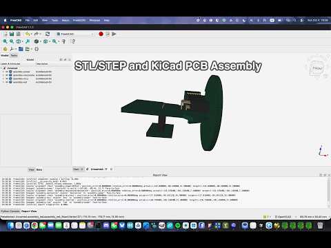
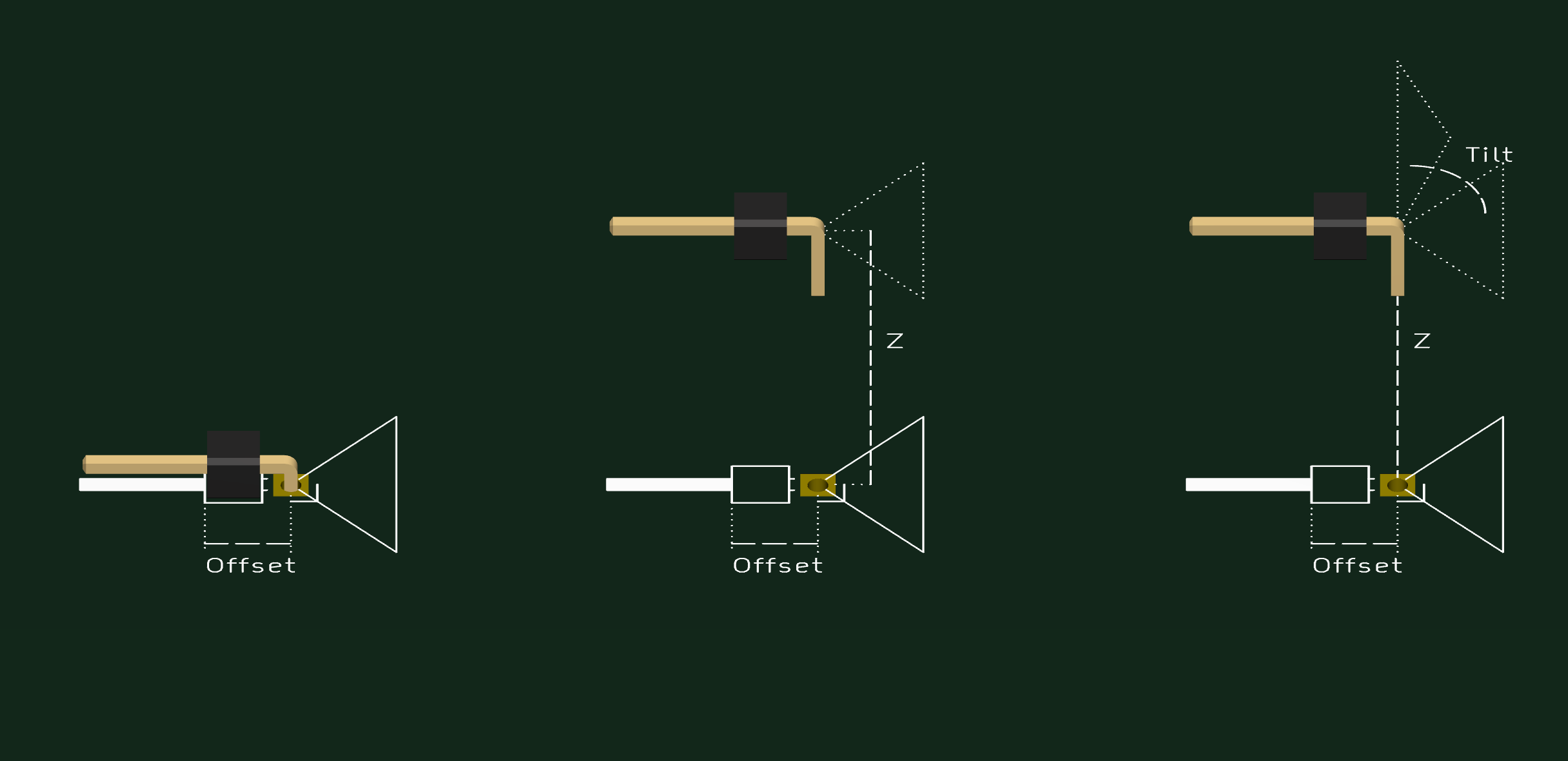
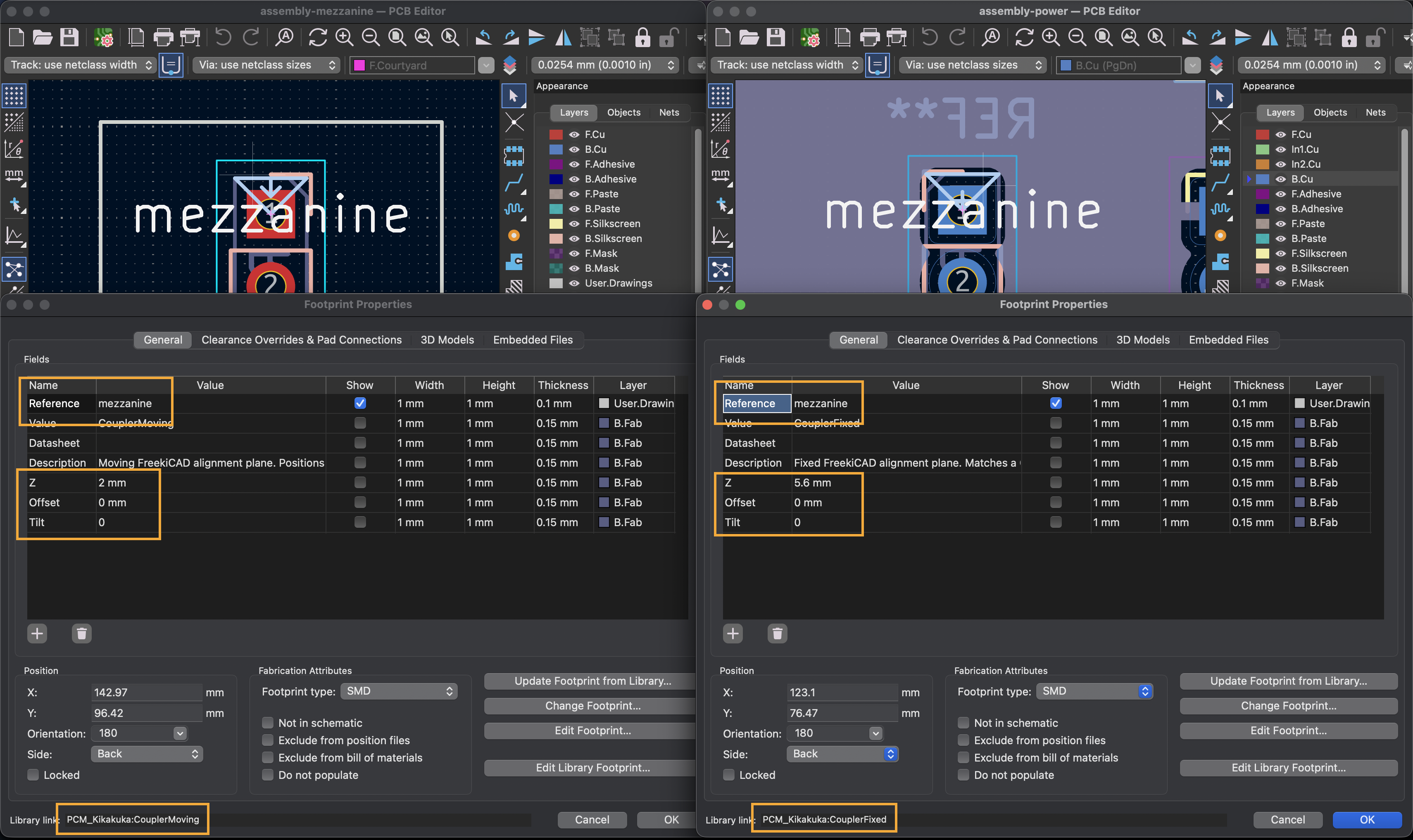
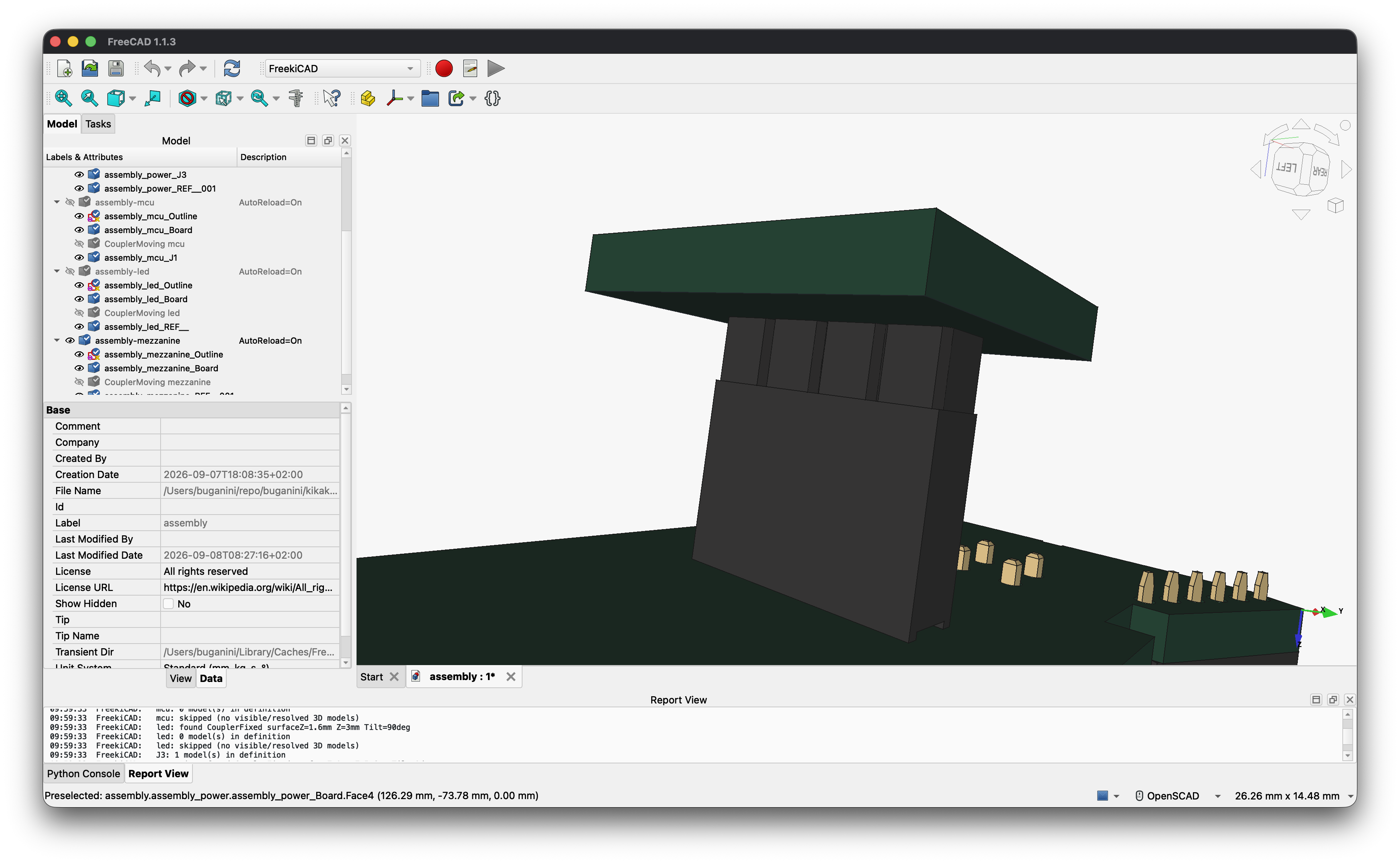
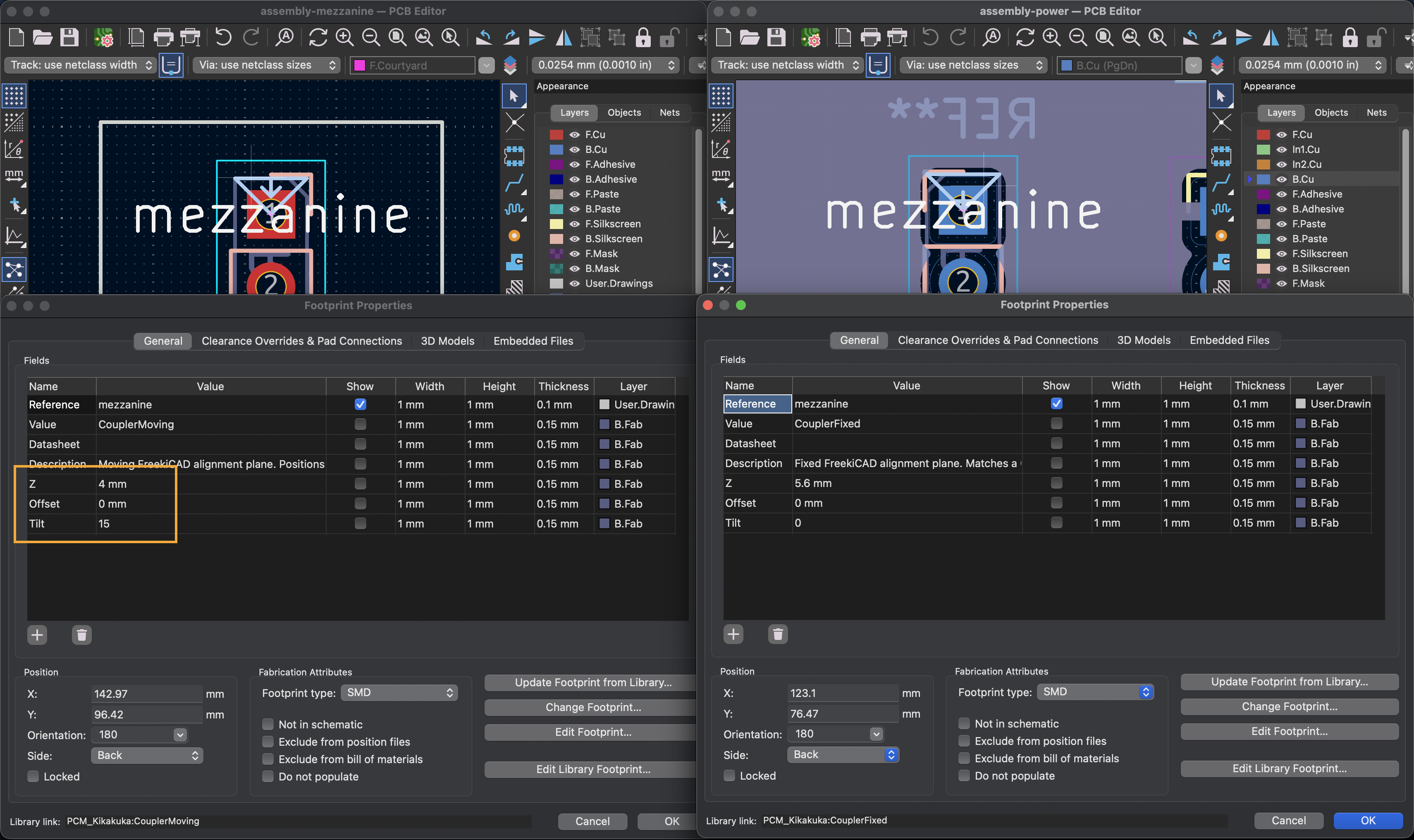
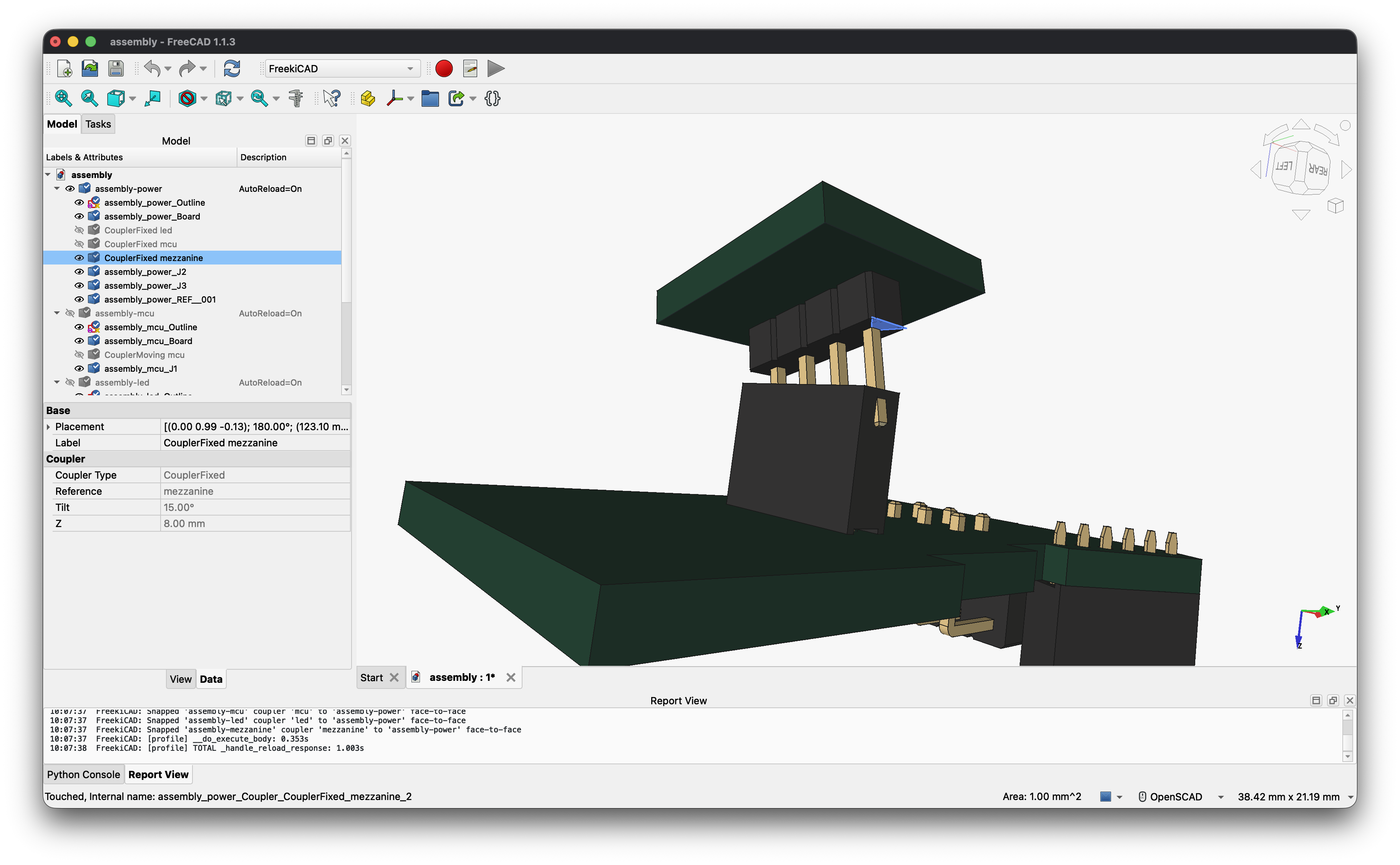
Coupler plane markers are available as child objects in FreeCAD and are hidden by default.
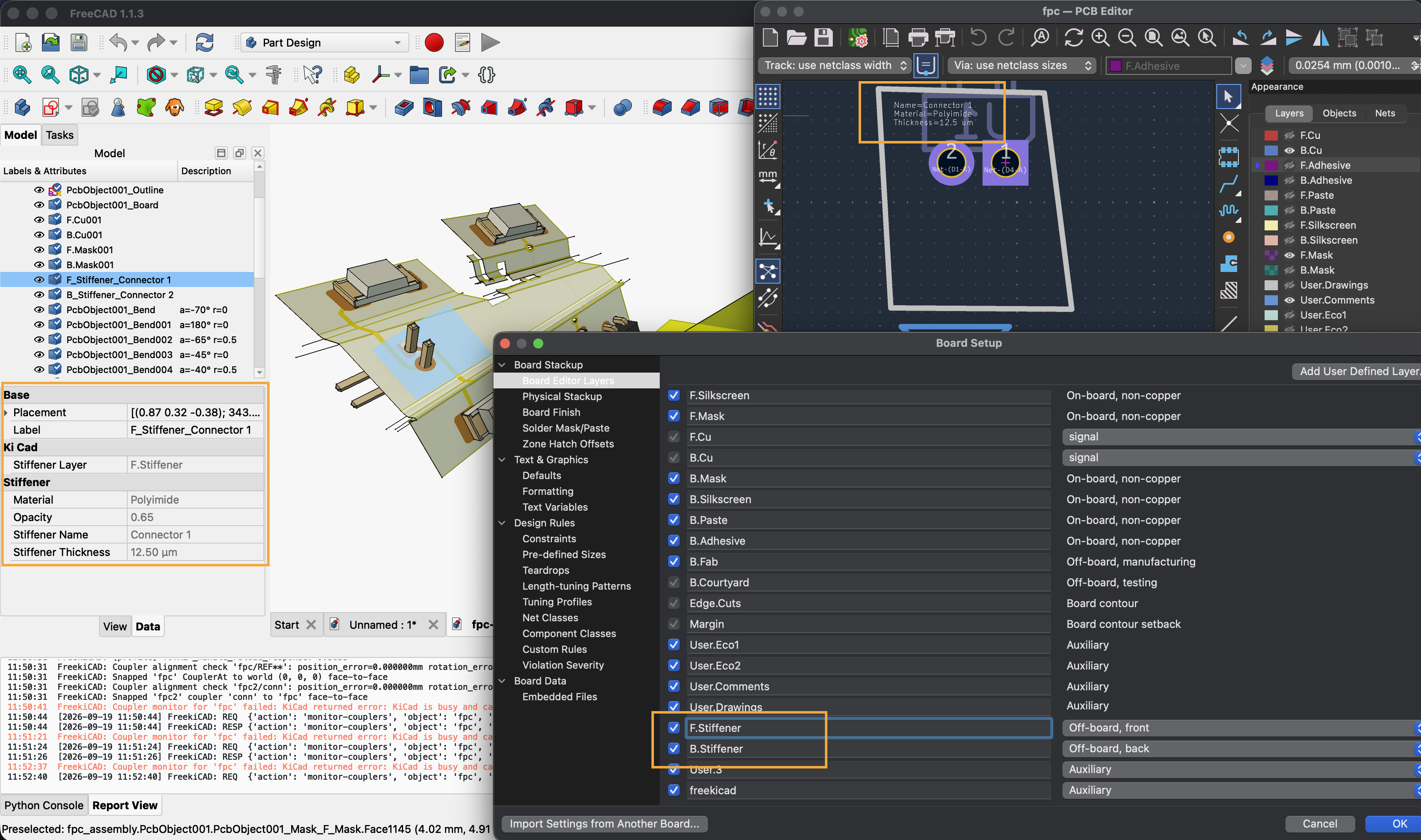
Rename KiCad user layers to F.Stiffener and/or B.Stiffener
(case-insensitive). Each closed rectangle, circle, polygon, or connected
line/arc outline is imported automatically as one stiffener area; the KiCad
display fill may be on or off.
Put one text annotation inside each area and separate properties with / or
newlines:
Name=Tail reinforcement
Material=Polyimide
Color=#C87518
Opacity=0.65
Thickness=25 um
Material and Thickness are required. Name, Color, and Opacity are
optional and property names are case-insensitive. A non-empty Name becomes
the suffix of the FreeCAD child name and label (F_Stiffener_<Name> or
B_Stiffener_<Name>) and is included in bend-overlap warnings. Thickness
accepts mm, cm, in, mil (0.001 in), and um; a unitless value is
interpreted as millimetres.
Invalid annotations, annotations outside an area, and areas with multiple annotations are reported as errors and skipped. Unannotated areas are skipped with a warning.
| Material | Default color | Default opacity |
|---|---|---|
FR4 | #C8B45A | 0.90 |
Polyimide | #C87518 | 0.65 |
Stainless_Steel | #A7ADB4 | 1.00 |
3M468 | #F2E3BD | 0.28 |
tesa8854 | #EEE8D8 | 0.45 |
3M9077 | #DDE8EE | 0.30 |
Other material names are accepted with a warning. When Color or Opacity
is omitted for an unlisted material, the corresponding Polyimide default is
used.
Front stiffeners extend outward from the front silkscreen plane; back
stiffeners extend outward from the back silkscreen plane. They remain rigid
during flex bending. Pad, via, and explicit mask-graphic openings on F.Mask
are cut through front stiffeners; B.Mask openings are cut through back
stiffeners. This happens even when ImportSolderMask is disabled. If a
stiffener overlaps the full bend band, FreekiCAD prints a warning containing
the stiffener name, bend name, and overlap area.
Stiffener thickness is additive outside the finished PCB and is never counted in or subtracted from the board body.
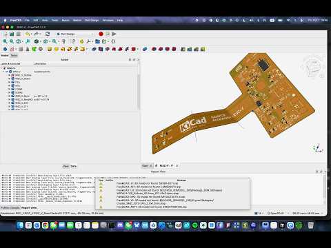
Manual bending checks are currently done with these sample boards:
For the implementation details of the bending pipeline, see FreekiCAD/ARCHITECTURE.md.
The KiCad library is stored under kicad-addon/library.
You can install it from Kikakuka's Integration tab. For a manual installation,
add kicad-addon/library/footprints/Kikakuka.pretty
to KiCad's footprint library table (for example, as Kikakuka). Its
Kikakuka.3dshapes directory
contains the unit-cube placeholder and optional coupler helper models.
Variable displays its Value on the board. In the Kikakuka Fabrication Planner, use build-variant fields such as Value#Flag or Value#Option=Choice to show a value selected by the active build flags or options.StringTemplate formats its Value during Kikakuka Fabrication Planner export. Braced placeholders are replaced with matching footprint properties or build options after build-variant fields have been applied.CouplerFixed and CouplerMoving define matching planes for coupler-based PCB alignment. Give a pair the same reference and use their Z, Offset, and Tilt properties as needed.CouplerAt aligns its PCB to absolute FreeCAD world TargetX, TargetY, and TargetZ coordinates, all defaulting to zero. Place it on B.Cu for the usual behavior, where the PCB bottom surface is positioned at TargetZ; use F.Cu only to reference the top surface.For coupler length properties (Z, Offset, TargetX, TargetY, and TargetZ), unitless values are millimetres; supported suffixes are mm, cm, in, mil, and um/µm. Tilt is in degrees and may optionally use deg or °.
All three coupler footprints use the Unspecified type, placing their helper models under Virtual Models in KiCad's 3D Viewer.
The separate Kikakuka Tools IPC plugin provides Coupler 3D Viewer and Hide Couplers actions. Coupler 3D Viewer applies each coupler's Z, Tilt, and Offset to its helper model and opens KiCad's 3D Viewer; Hide Couplers marks these models hidden without removing them and also opens the Viewer. Populate Placeholder 3D Models likewise opens the Viewer after populating models. To omit couplers from STEP export, enable Ignore 'Unspecified' components.
Kikakuka is mainly built on top of KiKit, Shapely, modified pcb-tools, OpenCV, pypdfium2 and PUI.
Its FreeCAD integration is inspired by KiCadStepUp and KiConnect.
Kikakuka, formerly Kikit-UI, began as an interactive GUI for KiKit and later expanded to include a workspace manager. File-to-instance tracking was introduced to make navigation from the workspace manager to KiCad reliable, with the workspace manager initially serving as the central orchestrator. After FreekiCAD was introduced, that mechanism evolved into CADhoc, a mesh of peer nodes running in Kikakuka and FreekiCAD without a permanent central orchestrator. The mesh also includes a client-only node in the KiCad add-on. CADhoc maintains a shared view of KiCad and FreeCAD instances and their open documents, so navigation no longer depends on the workspace manager.
Make sure your python can import pcbnew
> python3 -c "import pcbnew; print(pcbnew._pcbnew)"
<module '_pcbnew' from '/usr/lib/python3/dist-packages/_pcbnew.so'>
On macOS, I have to use the python interpreter bundled with KiCAD
PYTHON=/Applications/KiCad/KiCad.app/Contents/Frameworks/Python.framework/Versions/Current/bin/python3On Linux, you should be able to just use the your default python3
PYTHON=python3Create a virtual environment and install dependencies
${PYTHON} -m venv --system-site-packages env
./env/bin/pip3 install -r requirements.txt
On Debian/Ubuntu, PySide6's X11 platform plugin also needs these system libraries:
sudo apt install libxcb-cursor0 libxkbcommon-x11-0 libxcb-icccm4 libxcb-image0 libxcb-keysyms1 libxcb-render-util0 libxcb-xkb1Kikakuka uses opencv-python-headless for image processing and PySide6 for its
windows. If an existing environment has opencv-python installed, replace it
before reinstalling requirements (both packages provide the same cv2 module):
./env/bin/pip3 uninstall opencv-python
./env/bin/pip3 install -r requirements.txt
Update submodule
git submodule update --init --recursiveRun
./env/bin/python3 -m kikakuka
# Equivalent directory entry point:
./env/bin/python3 kikakuka/On Windows the Python interpreter is at C:\Program Files\KiCad\10.0\bin\python.exe.
But however in my Windows environment venv is not working properly, here is how I run it with everything installed in the KiCad's environment.
# Powershell
# Initialize bundled submodules after cloning
git submodule update --init --recursive

# Git for Windows may check symlinks out as text files containing their target
# paths. Replace all tracked symlinks with physical files/directories so the
# source tree can run without Windows symlink support.
& .\tools\materialize-symlinks.ps1

&"C:\Program Files\KiCad\10.0\bin\python.exe" -m pip install -r requirements.txt
&"C:\Program Files\KiCad\10.0\bin\python.exe" -m kikakuka
The materialization only changes the working tree; Git still tracks those paths
as symlinks. Re-running the script refreshes the physical copies. If PowerShell
blocks local scripts, run
powershell -ExecutionPolicy Bypass -File .\tools\materialize-symlinks.ps1.
# Just open it
./env/bin/python3 -m kikakuka

# Start with PCB files
./env/bin/python3 -m kikakuka a.kicad_pcb b.kicad_pcb...

# Open KiCad files through the instance manager
./env/bin/python3 -m kikakuka --open a.kicad_pcb

# Run a foreground CADhoc node with request/mapping logs
./env/bin/python3 -m cadhoc
# The equivalent directory entry point is: ./env/bin/python3 cadhoc

# Open or focus a PCB and reload it from disk once its IPC API is ready
./env/bin/python3 -m kikakuka --open --fresh a.kicad_pcb
# In a mixed list, --fresh affects only .kicad_pcb files; schematics and
# projects are opened normally.

# Stop all same-user KiCad and FreeCAD GUI instances (not FreeCADCmd)
# Warning: unsaved work may be lost.
./env/bin/python3 -m kikakuka --killall

# Stop only one application (case-insensitive)
./env/bin/python3 -m kikakuka --killall freecadKikakukaTools -> Update Footprints from Library can bring back the footprint if the name matchesSelection Filter)| Qty | Value | Footprint | References |
|---|---|---|---|
| 2 | 22uF 1210 | Capacitor_SMD:C_1210_3225Metric | C14, C16 |
| 2 | PWR | TerminalBlock_Phoenix:TerminalBlock_Phoenix_PT-1,5-2-5.0-H_1x02_P5.00mm_Horizontal | J6, J7 |
| 1 | 0.1uF | Capacitor_SMD:C_0603_1608Metric | C18 |
| 1 | 100k | Resistor_SMD:R_0603_1608Metric | R23 |
| 1 | 10uF 50V 0805 | Capacitor_SMD:C_0805_2012Metric | C2 |
| 1 | 1uF | Capacitor_SMD:C_0603_1608Metric | C10 |
| 1 | 220nF 50V 0805 | Capacitor_SMD:C_0805_2012Metric | C15 |
| 1 | 24.9k | Resistor_SMD:R_0603_1608Metric | R24 |
| 1 | 8.2uH 4x4mm | Inductor_SMD:L_Changjiang_FNR4030S | L1 |
| 1 | LMR33630ADDAR | Package_SO:Texas_HSOP-8-1EP_3.9x4.9mm_P1.27mm_ThermalVias | U3 |
It measures 43.6 × 17.4 mm and has 4 copper layers, 1.6 mm thick.
12 parts. The full list of its parts is on this page, with links to each part's symbol and footprint where PCBKit's library has them.
From the buganini/Kikakuka repository on GitHub, at the commit this page was made from: the board is samples/dcdc/dcdc.kicad_pcb and its schematic samples/dcdc/dcdc.kicad_sch. PCBKit opens the board in the browser, with nothing to install.
Its repository publishes it under the MIT licence: you may reuse it on that licence's terms (keep the author's notice, and for a copyleft licence share your changes alike).
buganini/Kikakuka
Kikakuka — KiCad Workspace, Panelization, Build Variants, Differ & FreeCAD PCB Bending and Assembly

buganini/Kikakuka
Kikakuka — KiCad Workspace, Panelization, Build Variants, Differ & FreeCAD PCB Bending and Assembly

buganini/Kikakuka
Kikakuka — KiCad Workspace, Panelization, Build Variants, Differ & FreeCAD PCB Bending and Assembly

buganini/Kikakuka
Kikakuka — KiCad Workspace, Panelization, Build Variants, Differ & FreeCAD PCB Bending and Assembly

byrantech/laptop
anyon_e, a highly integrated, high end, open source laptop. Attempt the impossible.


BelaPlatform/Trill
Trill sensors are designed to bring beautiful touch interaction to digital projects. Trill sensors are available now on the Bela Shop and via Mouser Electronics.

marsairforce/breakout_boards
Small circuit boards to assist with breadboard prototyping with SMD packages.

ras-marques/ImmersiveGloves
I want to share how I am making vr gloves using 2 Tundra Trackers, 2 interface boards and 12 inertial sensors.