2 layers410.2 × 272.4 mm

 Bread80/Datapoint220019
Datapoint 2200 Schematics and Documents
Memory is an open-source printed circuit board by Bread80, from the Bread80/Datapoint2200 repository on GitHub. It is a 2-layer board of 133.4 × 201.3 mm with 173 parts on 120 nets, routed with 2,123 tracks and 355 vias.
It is built around the 74HCT245, Z21 and Z30. Its parts include 49 diodes, 48 resistors, 17 capacitors, 6 transistors and 3 ICs. It belongs with the retro computing and games boards of this library.

This is my project to transcribe the schematics for a Datapoint 2200 serial processor machine, reverse engineer them, and recreate the original hardware with added blinkenlights.
The repository contains schematics, PCB layout files, documents and software relevant to the 2200.
The schematics are in Kicad 5 format (at least until I make my peace with the UI in newer versions). To open them you may need to import the symbol library in Datapoint2200.lib and the Datapoint2200.pretty folder.
NOTES:
Some of the included files/PDFs:
Schematics for each board are in their own folder.
The following lists the key boards of the Datapoint 2200 and the current status of each board.
Status: Not transcribed.
Modulator for the tape drives
Status: Not transcribed yet.
Demodulator for the tape drives
Status: Not transcribed yet.
The system sequencer and output port/command decoder.
The schematic is split into the following files and functional units:
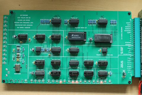
Status: A first revision board has been manufactured and works but has a couple of largely cosmetic issues, the worst of which is an incorrect footprint for the wide-body TTL chips. The PCB currently in the repository is the proposed next revision but which has not been tested - I'll have it manufactured when I know it is driving the rest of the system correctly.
The processor itself. The schematic is divided up as follows:
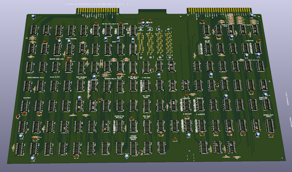
Status: The design has been tested in a logic emulator and appears to function correctly. A PCB layout has been made up and I'm currently adding LEDs (and establishing which signals should have LEDs) before sending the board for production.
Houses the keyswitches and multiplexing circuitry.
Status: Transcribed but not checked.
This board houses the circuitry for driving the CRT, and also some TTL logic spilled over from the Display Control board.
Status: The TTL circuits have been transcribed. I'm proposing to replace the CRT circuitry with something capable of driving a suitable modern display (ie. something microcontroller based).
The 'video card'. Contains video memory, character generator and display driver. The board also controls the reading of data from the keyboard.
The schematic is divided as follows
Status: Transcribed and checked (but not validated).
Contains the logic for scanning the keyboard, latching returned keypresses, and outputting characted codes in ASCII.
Contains the following modules:
Status: Transcribed and checked but not validated.
Houses the Intel 1405 shift memories ICs used by the processor and related row and column decoders.
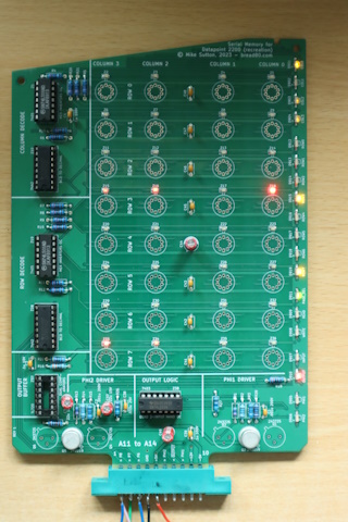
Status: Transcribed and first revision boards manufactured. The recreated PCBs include solder links to enable the memory to be operated at TTL voltage levels. Note: The board has not been tested with actual 1405 chips. Note: The 1405 ICs require a lot of power. The original PCBs are heavily engineered to be able to supply this power, and include a pair of bus bars for power distribution. The recreated PCBs have not been engineered to the same standards and shift should not be used with shift memories.
The 'backplane' into which many of the above boards slot (A1 to A9 except A6) or connect.
Status: Not transcribed yet
(Other board numbers are for smaller boards such as those in the tape machines, speaker mountings etc).
These are mainly notes for myself to keep things consistent between boards.
Components: LEDs, side facing: Datapoint2200:LED_Dialight_597_xxxx_407F_SMT_RA_3mmx2mmx1mm (custom component and footprint in Datapoint2200 library)
Footprints: Decoupling capacitors: Capacitor_THT:C_Disc_D7.0mm_W2.5mm_P5.00mm Resistors (through hole): Resistor_THT:R_Axial_DIN0207_L6.3mm_D2.5mm_P10.16mm_Horizontal Resistors (surface mount): Decoder uses 0805: Resistor_SMD:R_0805_2012Metric_Pad1.20x1.40mm_HandSolder (other boards will vary!) Mounting holes: MountingHole:MountingHole_3.2mm_M3 Holes positioned 7x 25mils from board edges Buttons (side mounted): Button_Switch_THT:SW_Tactile_SPST_Angled_PTS645Vx58-2LFS (exact model to be clarified)
Silkscreen: All silkscreen placed on a 25mil (0.6250mm) grid Section titles font size: W1.5 H1.5 Thickness: .25 Text for ICs: Top left: chip code (e.g. 7493), stated with original 74 series (no LS, HCT etc) Top right: reference code (e.g Z19) Below: chip description, centred. Use summary from datasheet where possible Text for edge connector pins: Left (right on reverse) aligned to edge connector Use a < or > at connector end to indicate signal direction Positioned 50mil (2x0.6350mm) from connector pad Edge connector pin numbers: Label first and last pin on each side. Font size: H1.5 H1.5 Thickness: 0.25 Position: centred aligned 8x 25mil horizontally from edge of connector pads 4x 25mil vertically from centre of first pad Board identifier (e.g. A4) Font size: H2 W2 Thickness: 0.35, orientation 90 degrees (i.e. from bottom to top) (Orientation valid for 'main' PCBs) Positioning: Centre aligned, 6x 25mils from board edge, 6x 25mils from edge of edge connector Lines: Section separators: 0.5mm width Sub-section separators: 0.12mm width
*74x00 4 quad 2-input NAND gate 14 SN74LS00 *74x02 4 quad 2-input NOR gate 14 SN74LS02 *74x03 4 quad 2-input NAND gate open-collector 14 SN74LS03 *74x04 6 hex inverter gate 14 SN74LS04 *74x05 6 hex inverter gate open-collector 14 SN74LS05 **74x06 6 hex inverter gate open-collector 30 V / 40 mA 14 *74x08 4 quad 2-input AND gate 14 SN74LS08 *74x10 3 triple 3-input NAND gate 14 SN74LS10 *74x20 2 dual 4-input NAND gate 14 SN74LS20 *74x30 1 single 8-input NAND gate 14 SN74LS30 **74x37 4 quad 2-input NAND gate driver NO=30 14 SN74LS37 **74x40 2 dual 4-input NAND gate driver NO=30 14 SN74LS40 *74x42 1 BCD to decimal decoder 16 SN74LS42 *74x73 2 dual J-K flip-flop, asynchronous clear 14 SN54LS73A *74x74 2 dual D positive edge triggered flip-flop, asynchronous preset and clear 14 SN74LS74A *74x85 1 4-bit magnitude comparator 16 SN74LS85 *74x89 1 64-bit RAM (16x4), 4 data inputs, 4 inverted data outputs open-collector 16 SN7489 *74x95 1 4-bit shift register, parallel in, parallel out, serial input; different pinout for 74L95 14 *74x151 1 8-line to 1-line data selector/multiplexer 16 SN74151A *74x153 2 dual 4-line to 1-line data selector/multiplexer, non-inverting outputs 16 SN74153 *74x164 1 8-bit serial-in parallel-out (SIPO) shift register, asynchronous clear, not output latch 14 SN74164 *74x193 1 synchronous presettable up/down 4-bit binary counter, clear 16 SN74193
| Qty | Value | Footprint | References |
|---|---|---|---|
| 32 | 1405 | DataPoint_2200:TO-99-10 | Z2, Z11, Z12, Z13, Z14, Z15, Z16, Z17, Z18, Z20, Z21, Z22, Z23, Z24, Z25, Z26 +16 |
| 23 | 470R | Resistor_SMD:R_0805_2012Metric_Pad1.20x1.40mm_HandSolder | R901, R902, R903, R904, R905, R906, R907, R908, R909, R910, R911, R912, R913, R914, R915, R916 +7 |
| 13 | 2k2 | Resistor_THT:R_Axial_DIN0207_L6.3mm_D2.5mm_P10.16mm_Horizontal | R4, R5, R6, R7, R8, R9, R10, R11, R12, R18, R19, R20, R21 |
| 9 | .1u 100V | Capacitor_THT:C_Disc_D4.7mm_W2.5mm_P5.00mm | C6, C39, C41, C42, C43, C45, C46, C47, C48 |
| 3 | 22u 15V | Capacitor_THT:CP_Radial_D5.0mm_P2.50mm | C36, C37, C49 |
| 3 | 74HCT245 | Package_SO:TSSOP-20_4.4x6.5mm_P0.65mm | U904, U905, U906 |
| 2 | .001u 200V | Capacitor_THT:C_Disc_D4.7mm_W2.5mm_P5.00mm | C1, C2 |
| 2 | 100 | Resistor_THT:R_Axial_DIN0207_L6.3mm_D2.5mm_P10.16mm_Horizontal | R2, R14 |
| 2 | 1k | Resistor_THT:R_Axial_DIN0207_L6.3mm_D2.5mm_P10.16mm_Horizontal | R25, R28 |
| 2 | 220 | Resistor_THT:R_Axial_DIN0207_L6.3mm_D2.5mm_P10.16mm_Horizontal | R1, R13 |
| 2 | 2N2219 | Package_TO_SOT_THT:TO-39-3 | Q2, Q5 |
| 2 | 2N3725 | Package_TO_SOT_THT:TO-39-3 | Q1, Q6 |
| 2 | 2N3726 | Package_TO_SOT_THT:TO-39-3 | Q3, Q4 |
| 2 | 680 | Resistor_THT:R_Axial_DIN0207_L6.3mm_D2.5mm_P10.16mm_Horizontal | R3, R15 |
| 2 | 6R8 | Resistor_THT:R_Axial_DIN0207_L6.3mm_D2.5mm_P10.16mm_Horizontal | R26, R27 |
| 2 | 7405 | Package_DIP:DIP-14_W7.62mm_Socket | Z1, Z19 |
| 2 | 7442 | Package_DIP:DIP-16_W7.62mm_Socket | Z10, Z28 |
| 2 | MountingHole | MountingHole:MountingHole_3.2mm_M3 | H901, H902 |
| 1 | .033u 25V | Capacitor_THT:C_Disc_D4.7mm_W2.5mm_P5.00mm | C38 |
| 1 | .1u 10V | Capacitor_THT:C_Disc_D4.7mm_W2.5mm_P5.00mm | C3 |
| 1 | 330 | Resistor_THT:R_Axial_DIN0207_L6.3mm_D2.5mm_P10.16mm_Horizontal | R16 |
| 1 | 470 | Resistor_THT:R_Axial_DIN0207_L6.3mm_D2.5mm_P10.16mm_Horizontal | R22 |
| 1 | 68u 15V | Capacitor_THT:CP_Radial_D6.3mm_P2.50mm | C44 |
| 1 | 7403 | Package_DIP:DIP-14_W7.62mm_Socket | Z38 |
| 1 | COL0 | DataPoint_2200:LED_Dialight_597_xxxx_407F_SMT_RA_3mmx2mmx1mm | D901 |
| 1 | COL1 | DataPoint_2200:LED_Dialight_597_xxxx_407F_SMT_RA_3mmx2mmx1mm | D902 |
| 1 | COL2 | DataPoint_2200:LED_Dialight_597_xxxx_407F_SMT_RA_3mmx2mmx1mm | D903 |
| 1 | COL3 | DataPoint_2200:LED_Dialight_597_xxxx_407F_SMT_RA_3mmx2mmx1mm | D904 |
| 1 | COMPARATOR | Jumper:SolderJumper-2_P1.3mm_Open_RoundedPad1.0x1.5mm | JP907 |
| 1 | Edge_Bottom | DataPoint_2200:EdgeConn_10_Pin_Pitch_3.96mm | J1 |
| 1 | Edge_Top | DataPoint_2200:EdgeConn_10_Pin_Pitch_3.96mm | J2 |
| 1 | INPUT | DataPoint_2200:LED_Dialight_597_xxxx_407F_SMT_RA_3mmx2mmx1mm | D907 |
| 1 | OUTPUT | DataPoint_2200:LED_Dialight_597_xxxx_407F_SMT_RA_3mmx2mmx1mm | D910 |
| 1 | OUTPUT_MEM | Jumper:SolderJumper-2_P1.3mm_Open_RoundedPad1.0x1.5mm | JP906 |
| 1 | PAGE_SEL | DataPoint_2200:LED_Dialight_597_xxxx_407F_SMT_RA_3mmx2mmx1mm | D911 |
| 1 | PHI1 | DataPoint_2200:LED_Dialight_597_xxxx_407F_SMT_RA_3mmx2mmx1mm | D905 |
| 1 | PHI1 Driver | Jumper:SolderJumper-2_P1.3mm_Open_RoundedPad1.0x1.5mm | JP901 |
| 1 | PHI2 | DataPoint_2200:LED_Dialight_597_xxxx_407F_SMT_RA_3mmx2mmx1mm | D906 |
| 1 | PHI2 Driver | Jumper:SolderJumper-2_P1.3mm_Open_RoundedPad1.0x1.5mm | JP903 |
| 1 | READ | DataPoint_2200:LED_Dialight_597_xxxx_407F_SMT_RA_3mmx2mmx1mm | D909 |
| 1 | ROW0 | DataPoint_2200:LED_Dialight_597_xxxx_407F_SMT_RA_3mmx2mmx1mm | D912 |
| 1 | ROW1 | DataPoint_2200:LED_Dialight_597_xxxx_407F_SMT_RA_3mmx2mmx1mm | D913 |
| 1 | ROW2 | DataPoint_2200:LED_Dialight_597_xxxx_407F_SMT_RA_3mmx2mmx1mm | D914 |
| 1 | ROW3 | DataPoint_2200:LED_Dialight_597_xxxx_407F_SMT_RA_3mmx2mmx1mm | D915 |
| 1 | ROW4 | DataPoint_2200:LED_Dialight_597_xxxx_407F_SMT_RA_3mmx2mmx1mm | D916 |
| 1 | ROW5 | DataPoint_2200:LED_Dialight_597_xxxx_407F_SMT_RA_3mmx2mmx1mm | D917 |
| 1 | ROW6 | DataPoint_2200:LED_Dialight_597_xxxx_407F_SMT_RA_3mmx2mmx1mm | D918 |
| 1 | ROW7 | DataPoint_2200:LED_Dialight_597_xxxx_407F_SMT_RA_3mmx2mmx1mm | D919 |
| 1 | TL720 | Package_DIP:DIP-14_W7.62mm_Socket | Z37 |
| 1 | WRITE | DataPoint_2200:LED_Dialight_597_xxxx_407F_SMT_RA_3mmx2mmx1mm | D908 |
| 1 | Z11 | LED_SMD:LED_0805_2012Metric_Pad1.15x1.40mm_HandSolder | D931 |
| 1 | Z12 | LED_SMD:LED_0805_2012Metric_Pad1.15x1.40mm_HandSolder | D930 |
| 1 | Z13 | LED_SMD:LED_0805_2012Metric_Pad1.15x1.40mm_HandSolder | D929 |
| 1 | Z14 | LED_SMD:LED_0805_2012Metric_Pad1.15x1.40mm_HandSolder | D928 |
| 1 | Z15 | LED_SMD:LED_0805_2012Metric_Pad1.15x1.40mm_HandSolder | D935 |
| 1 | Z16 | LED_SMD:LED_0805_2012Metric_Pad1.15x1.40mm_HandSolder | D934 |
| 1 | Z17 | LED_SMD:LED_0805_2012Metric_Pad1.15x1.40mm_HandSolder | D933 |
| 1 | Z18 | LED_SMD:LED_0805_2012Metric_Pad1.15x1.40mm_HandSolder | D932 |
| 1 | Z2 | LED_SMD:LED_0805_2012Metric_Pad1.15x1.40mm_HandSolder | D923 |
| 1 | Z20 | LED_SMD:LED_0805_2012Metric_Pad1.15x1.40mm_HandSolder | D939 |
| 1 | Z21 | LED_SMD:LED_0805_2012Metric_Pad1.15x1.40mm_HandSolder | D938 |
| 1 | Z22 | LED_SMD:LED_0805_2012Metric_Pad1.15x1.40mm_HandSolder | D937 |
| 1 | Z23 | LED_SMD:LED_0805_2012Metric_Pad1.15x1.40mm_HandSolder | D936 |
| 1 | Z24 | LED_SMD:LED_0805_2012Metric_Pad1.15x1.40mm_HandSolder | D943 |
| 1 | Z25 | LED_SMD:LED_0805_2012Metric_Pad1.15x1.40mm_HandSolder | D942 |
| 1 | Z26 | LED_SMD:LED_0805_2012Metric_Pad1.15x1.40mm_HandSolder | D941 |
| 1 | Z27 | LED_SMD:LED_0805_2012Metric_Pad1.15x1.40mm_HandSolder | D940 |
| 1 | Z29 | LED_SMD:LED_0805_2012Metric_Pad1.15x1.40mm_HandSolder | D947 |
| 1 | Z3 | LED_SMD:LED_0805_2012Metric_Pad1.15x1.40mm_HandSolder | D922 |
| 1 | Z30 | LED_SMD:LED_0805_2012Metric_Pad1.15x1.40mm_HandSolder | D946 |
| 1 | Z31 | LED_SMD:LED_0805_2012Metric_Pad1.15x1.40mm_HandSolder | D945 |
| 1 | Z32 | LED_SMD:LED_0805_2012Metric_Pad1.15x1.40mm_HandSolder | D944 |
| 1 | Z33 | LED_SMD:LED_0805_2012Metric_Pad1.15x1.40mm_HandSolder | D951 |
| 1 | Z34 | LED_SMD:LED_0805_2012Metric_Pad1.15x1.40mm_HandSolder | D950 |
| 1 | Z35 | LED_SMD:LED_0805_2012Metric_Pad1.15x1.40mm_HandSolder | D949 |
| 1 | Z36 | LED_SMD:LED_0805_2012Metric_Pad1.15x1.40mm_HandSolder | D948 |
| 1 | Z4 | LED_SMD:LED_0805_2012Metric_Pad1.15x1.40mm_HandSolder | D921 |
| 1 | Z5 | LED_SMD:LED_0805_2012Metric_Pad1.15x1.40mm_HandSolder | D920 |
| 1 | Z6 | LED_SMD:LED_0805_2012Metric_Pad1.15x1.40mm_HandSolder | D927 |
| 1 | Z7 | LED_SMD:LED_0805_2012Metric_Pad1.15x1.40mm_HandSolder | D926 |
The 169 most common of 173 parts.
It measures 133.4 × 201.3 mm and has 2 copper layers, 1.6 mm thick.
173 parts, built around the 74HCT245, Z21 and Z30. The full list of its parts is on this page, with links to each part's symbol and footprint where PCBKit's library has them.
From the Bread80/Datapoint2200 repository on GitHub, at the commit this page was made from: the board is Memory/Memory.kicad_pcb. PCBKit opens the board in the browser, with nothing to install.
Its repository states no licence, so its author keeps all rights: ask Bread80 before reusing the design.


schlae/snark-barker-mca
A Sound Blaster compatible sound card for Micro Channel bus computers

artemisamsx/artemisa
Schematics, PCB designs and HDL simulations to build a 8-bits MSX computer

mecparts/PicoWiFiModem
A Pico W based RS232 <-> WiFi modem with Hayes AT style commands and LED indicators