
2 layers58.4 × 36.8 mm
Bf-018a
botanicfields/KiCad6-Environment
My symbols, my footprints, my templates, etc. of KiCad6
22 parts5CC0-1.0

My symbols, my footprints, my templates, etc. of KiCad6
Bf-039 is an open-source printed circuit board by botanicfields, from the botanicfields/KiCad6-Environment repository on GitHub, published under the CC0-1.0 licence. It is a 2-layer board of 45.7 × 17.8 mm with 17 parts on 13 nets, routed with 99 tracks and 17 vias.
Its parts include 7 resistors, 4 connectors and 2 diodes. It belongs with the 8051 (CH55x, STC, AT89) boards of this library.
My symbols, my footprints, my templates, etc. of KiCad6
KiCad6 による基板の設計時に作成したライブラリやテンプレートを置いています。
「シンボルエディター」で作成したシンボルのライブラリです。
使用しているシンボルのうち、独自に作成したシンボルの全てを含みます。
「フットプリントエディター」で作成したフットプリントのライブラリです。
使用しているフットプリントのうち、独自に作成したフットプリントの全てを含みます。
「KiCadマネージャー」において「テンプレートから新規プロジェクトを作成..」で選択可能となる「ユーザーテンプレート」のデータです。
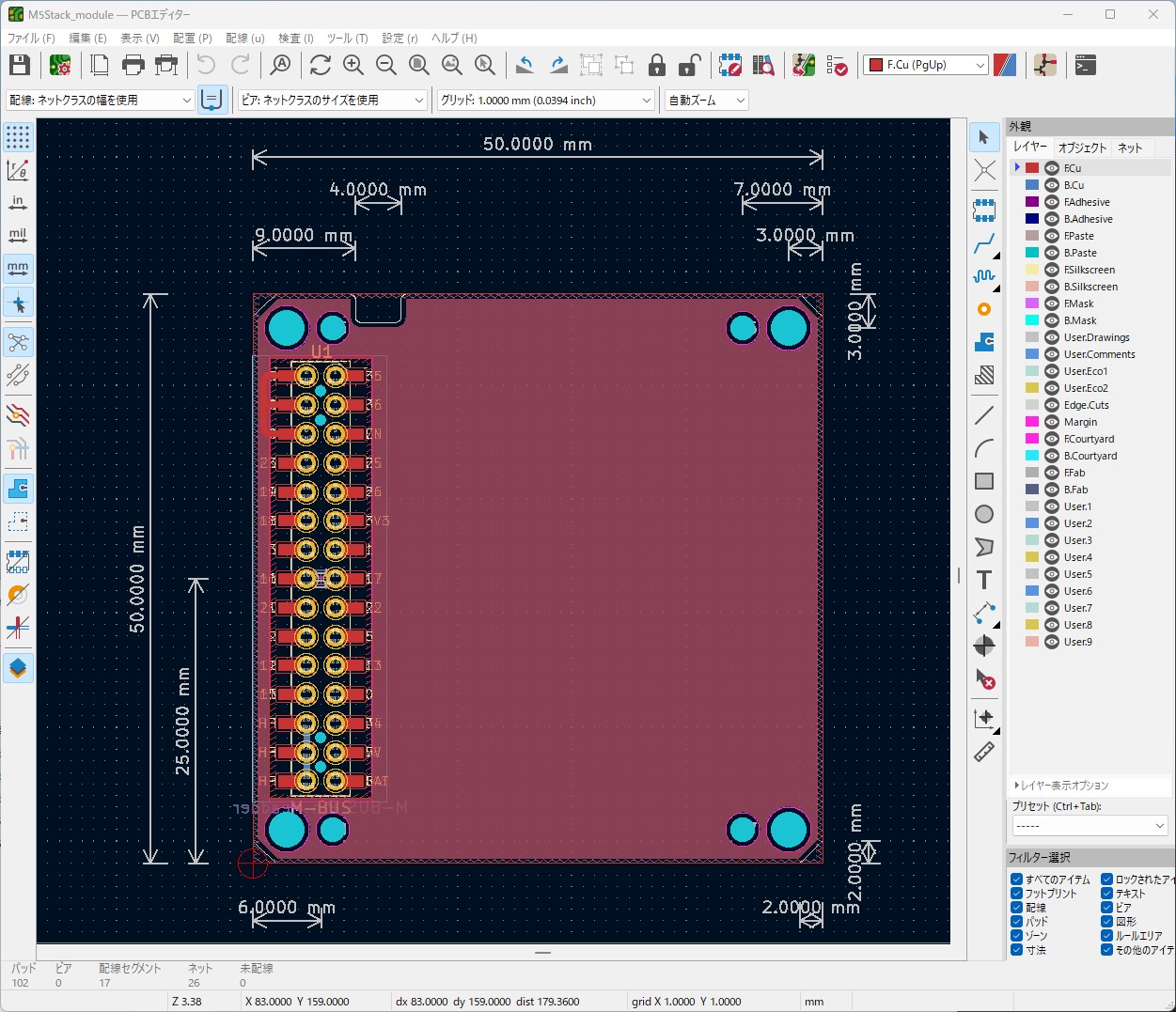
M5Stack用のモジュール基板のテンプレートです。M-BUSのピンヘッダーとピンソケットの両方を備え、モジュールの積み重ねに対応します。フレームにはM5Stack社のPROTOモジュールのモールドを流用することを想定しています。
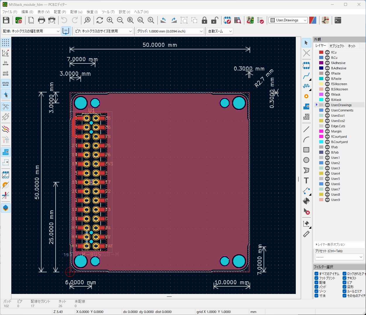
M5Stack用のモジュール基板のテンプレートです。M-BUSのピンヘッダーとピンソケットの両方を備え、モジュールの積み重ねに対応します。フレームにはFDMによるモールドを使用することを想定し、四隅に逃げがあります。
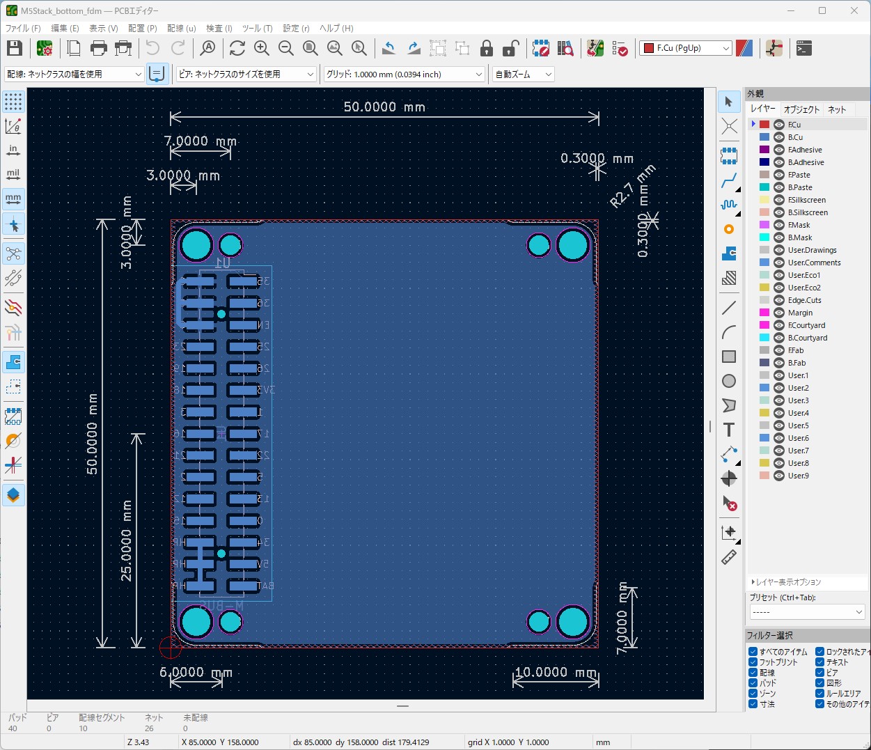
M5Stack用のボトム基板のテンプレートです。M-BUSのピンヘッダーがありますがピンソケットはありません。フレームにはFDMによるモールドを使用することを想定し、四隅に逃げがあります。
| Qty | Value | Footprint | References |
|---|---|---|---|
| 2 | 2.2k | Resistor_SMD:R_0603_1608Metric | R6, R7 |
| 2 | 5.1k | Resistor_SMD:R_0603_1608Metric | R2, R3 |
| 1 | 0.1 | Resistor_THT:R_Axial_DIN0207_L6.3mm_D2.5mm_P10.16mm_Horizontal | R1 |
| 1 | 100 | Resistor_SMD:R_0603_1608Metric | R4 |
| 1 | 1S4 | Diode_THT:D_DO-41_SOD81_P10.16mm_Horizontal | D1 |
| 1 | 220 | Resistor_SMD:R_0603_1608Metric | R5 |
| 1 | CH552 | Jumper:SolderJumper-2_P1.3mm_Open_RoundedPad1.0x1.5mm | JP3 |
| 1 | CS | Jumper:SolderJumper-2_P1.3mm_Open_RoundedPad1.0x1.5mm | JP2 |
| 1 | LED | LED_SMD:LED_0603_1608Metric | D2 |
| 1 | LOGO | @bf:BF@Logo_BotanicFields_2mm | G*** |
| 1 | SENSE | Connector_PinSocket_2.54mm:PinSocket_2x03_P2.54mm_Vertical | J4 |
| 1 | USB_A_PLUG | bf:BF@USB-4AM103 | J2 |
| 1 | USB_A_Receptacle | bf:BF@USB-4AF103BS | J3 |
| 1 | USB_C_Receptacle | bf:BF@USB-C-5077CR-16-SMC2-BK-TR | J1 |
| 1 | VF | Jumper:SolderJumper-2_P1.3mm_Open_RoundedPad1.0x1.5mm | JP1 |
botanicfields/KiCad6-Environment
My symbols, my footprints, my templates, etc. of KiCad6

botanicfields/KiCad6-Environment
My symbols, my footprints, my templates, etc. of KiCad6

botanicfields/KiCad6-Environment
My symbols, my footprints, my templates, etc. of KiCad6


hoglet67/RGBtoHDMI
Bare-metal Raspberry Pi project that provides pixel-perfect sampling of Retro Computer RGB/YUV video and conversion to HDMI


hackclub/OnBoard
💡 Join 1,000 teenagers and make your first PCB with a $100 grant!

DDeGonge/OS-ARM
This arm is not industrial and it will not be fast, but that is not my goal. But it will hopefully be a very nice looking arm fully capable of 6dof motion, cheap enough to keep it accessable but capable enough to…


It measures 45.7 × 17.8 mm and has 2 copper layers, 1.6 mm thick.
17 parts. The full list of its parts is on this page, with links to each part's symbol and footprint where PCBKit's library has them.
From the botanicfields/KiCad6-Environment repository on GitHub, at the commit this page was made from: the board is 6.0/projects/bf-039/bf-039.kicad_pcb and its schematic 6.0/projects/bf-018a/bf-018a.kicad_sch. PCBKit opens the board in the browser, with nothing to install.
Its repository publishes it under the CC0-1.0 licence: you may reuse it on that licence's terms (keep the author's notice, and for a copyleft licence share your changes alike).