Skip to the content
PCBKitNew board
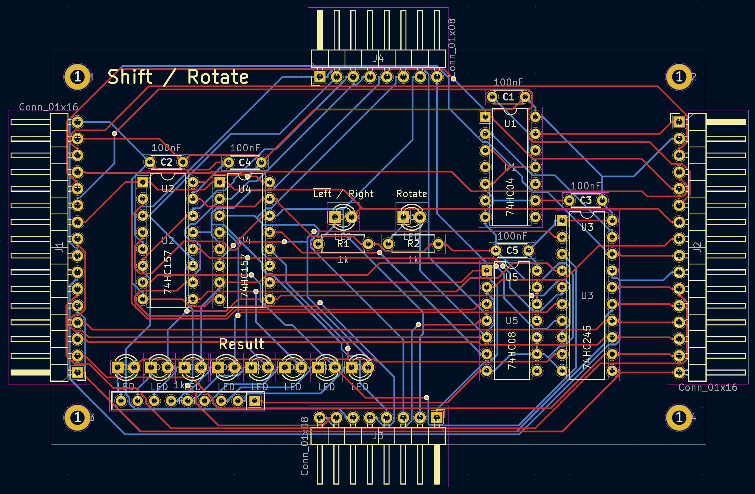
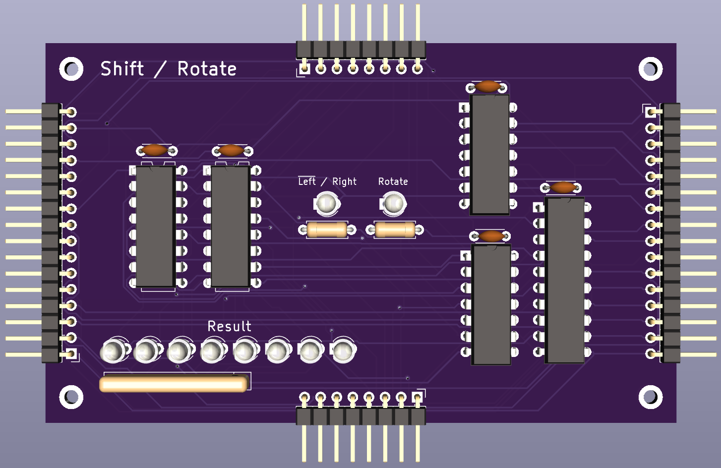
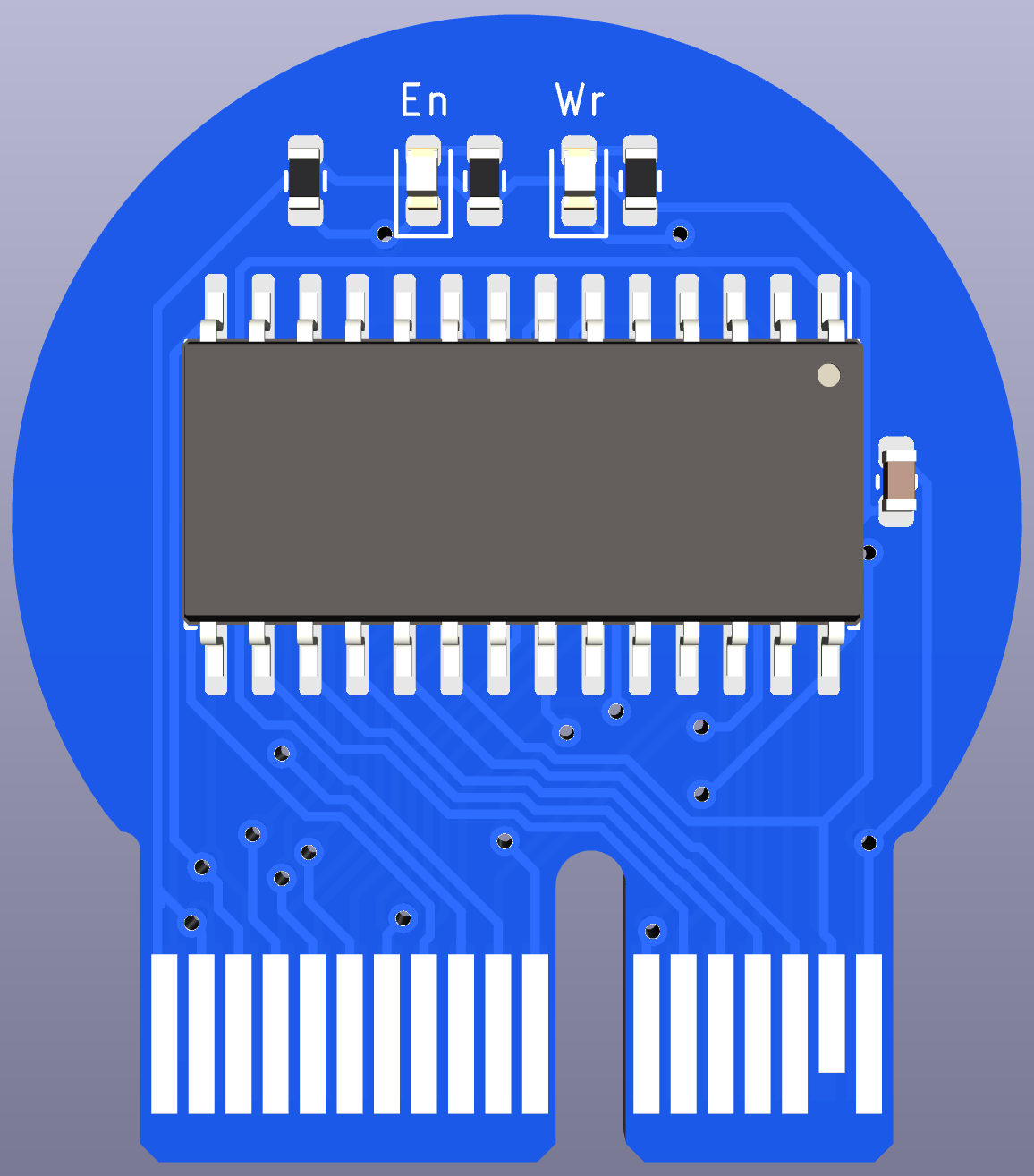
2 layers99.6 × 59.9 mmShift, the printed circuit board in 3D

An 8-bit CPU, made with TTL chips on custom, modular PCBs. Includes board designs, and Arduino code to program its instruction set and programs.

Size
99.6 × 59.9 mm
Copper layers
2
Thickness
1.6 mm
Parts
31
Nets
52
Pads
175
Tracks, vias
765, 20
Routed
Yes
KiCad
KiCad 7 (file 20221018)
Created
9 Feb 2021
Updated
20 Oct 2026

Overview

Shift is an open-source printed circuit board by benanderman, from the benanderman/spork-8 repository on GitHub, published under the MIT licence. It is a 2-layer board of 99.6 × 59.9 mm with 31 parts on 52 nets, routed with 765 tracks and 20 vias.

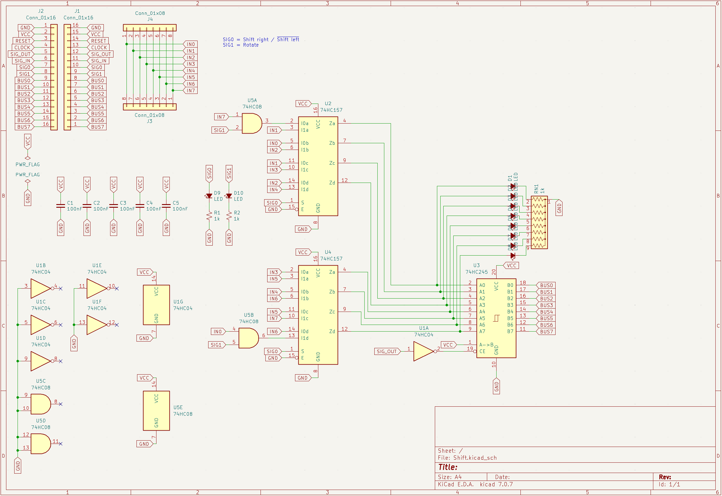
It is built around the 74HC245D, 74HC157D and 74HC04D, with the 74HC08D among its other parts. Its parts include 10 diodes, 5 capacitors, 5 ICs, 4 connectors and 2 resistors. It belongs with the retro computing and games boards of this library.

Main components

4

README

README.md

Spork-8

This is an 8-bit computer project, inspired by Ben Eater's 8-bit breadboard computer. It's made out of modular PCBs that plug into each other, and contain mostly 74HC-series chips (original 74LS). It runs code from an EEPROM (so it's only programmable from a computer), and has separate memory. It's meant to display what's happening, when running on a 555-timer or manually stepping, but also be capable enough to implement some sort of game, when using an oscillator as a clock.

For details about programming the Spork-8, see Programming.md.

Status of project

The project was originally completed in 2021 and mostly worked with 74LS-series chips, but it had some issues (see RevisionLog), and used way too much power.

In 2025, it was rebuilt with 74HC-series chips, and several improvements, an emulator, and peripheral boards. It had some issues, but mostly worked well.

In 2026, reliability was improved by adding ground planes to the bus boards and control board, the instruction set was improved, and much more complex programs were made.

Modules

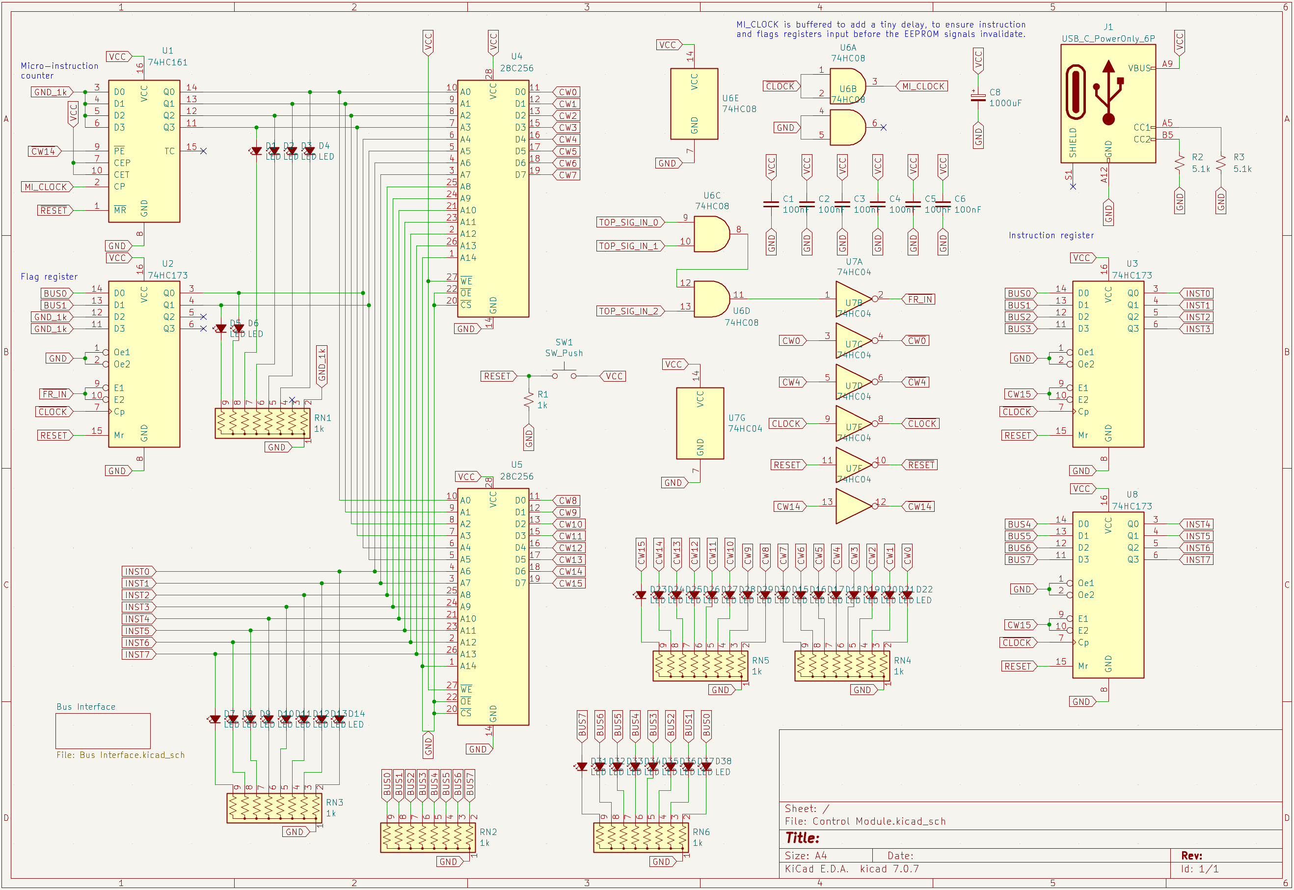
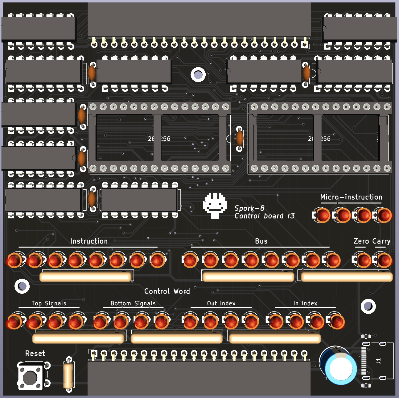
  • Control module: Coordinates everything else. Contains the micro-code EEPROMs, instruction register, micro-instruction counter, power input, reset button, and logic to interface with modules through bus boards.
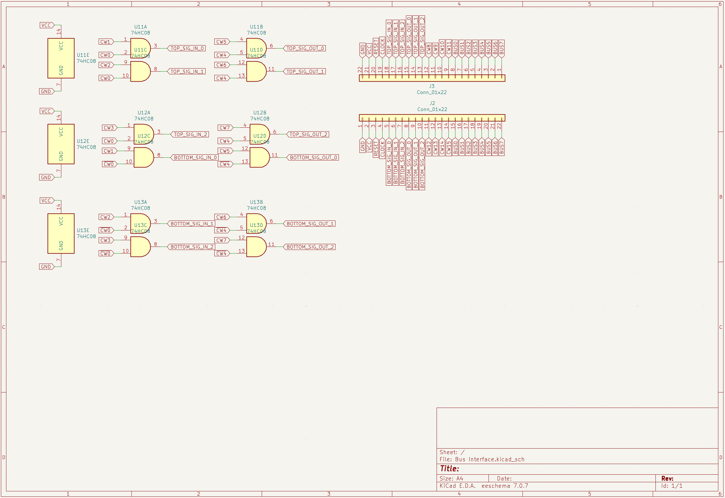
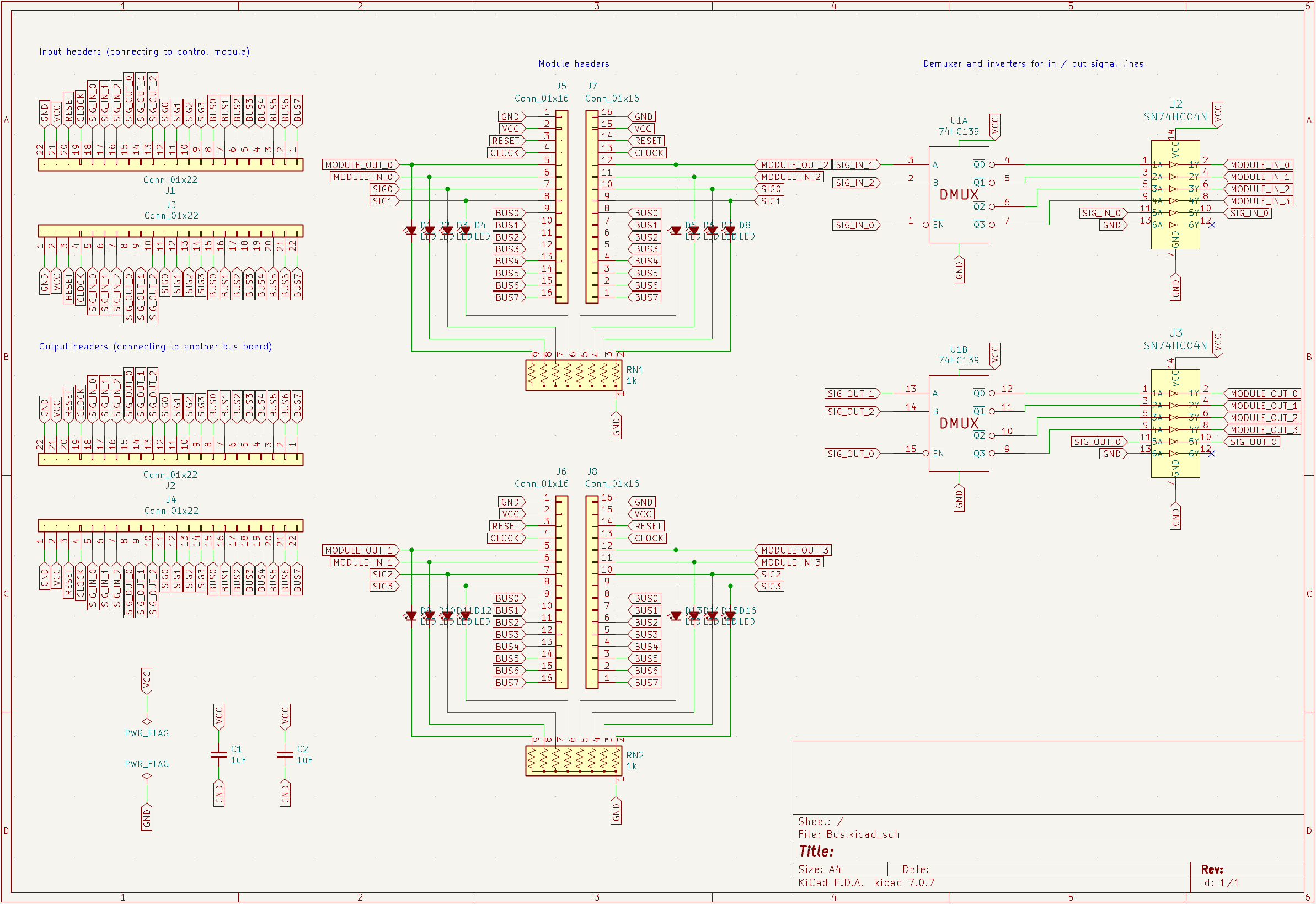
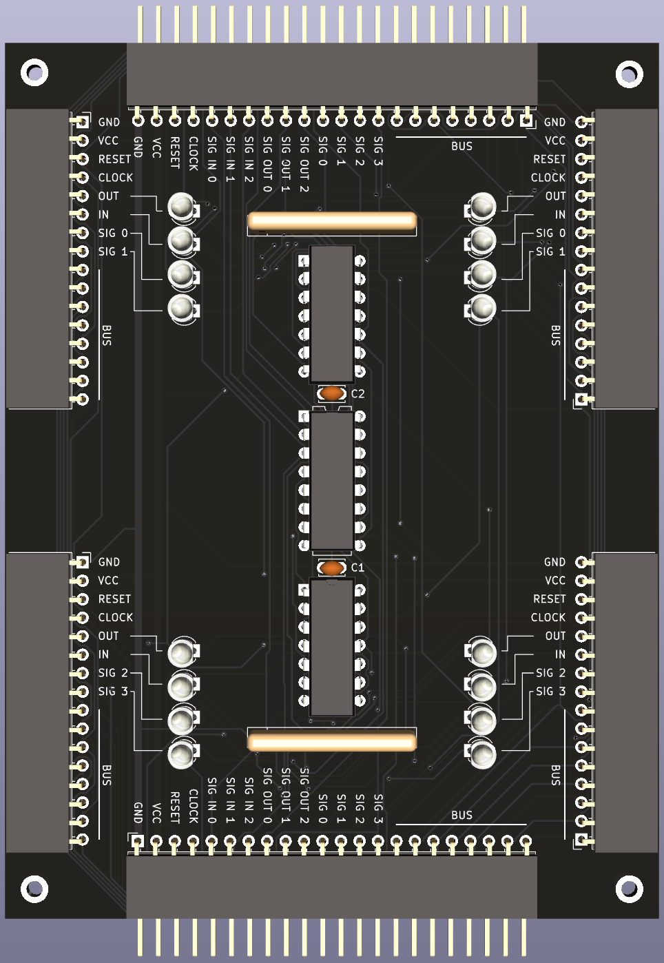
  • Bus: Four of these interface between the control module and up to 16 other modules. These demux three signal lines each for in/out enable signals to the four modules connected to each bus board. One bus board plugs into the top of the control module, and one into the bottom. Two more bus boards plug into the first two. The first in/out signal line selects between the two boards on top / bottom, and the one connected to the control module inverts the signal before passing it onto the other bus board.
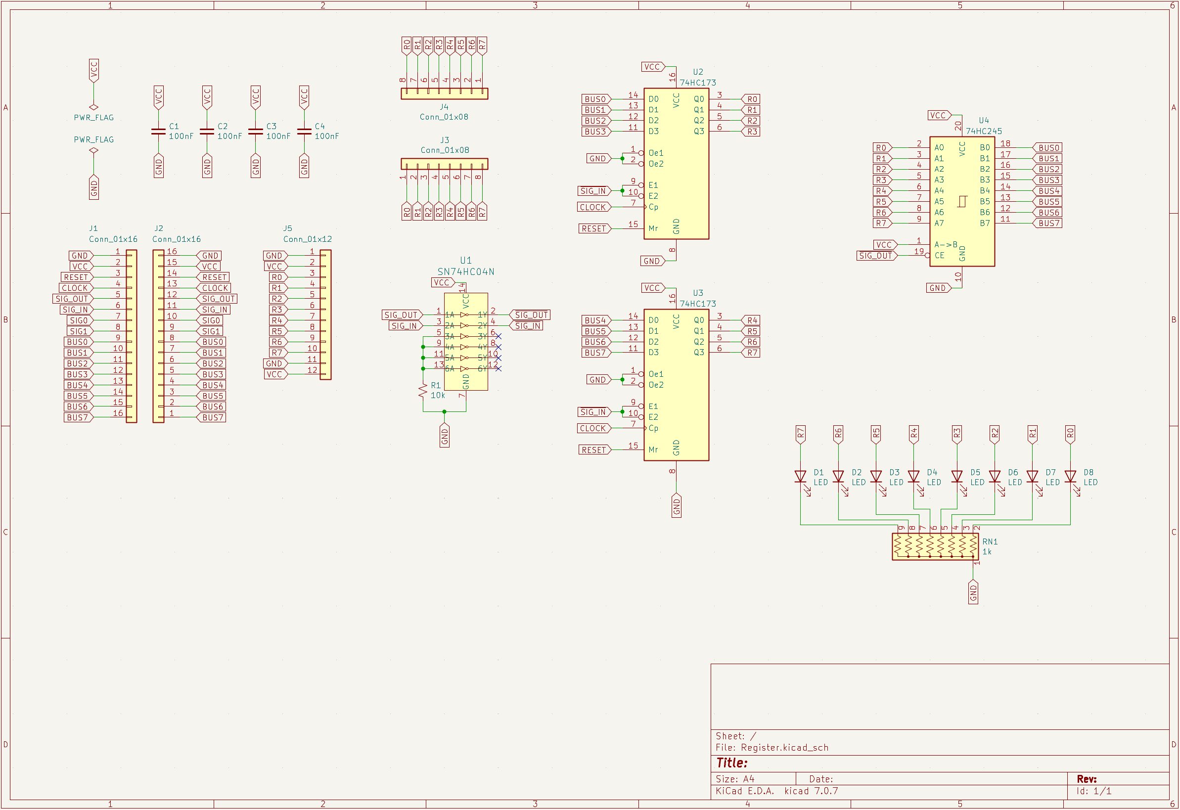
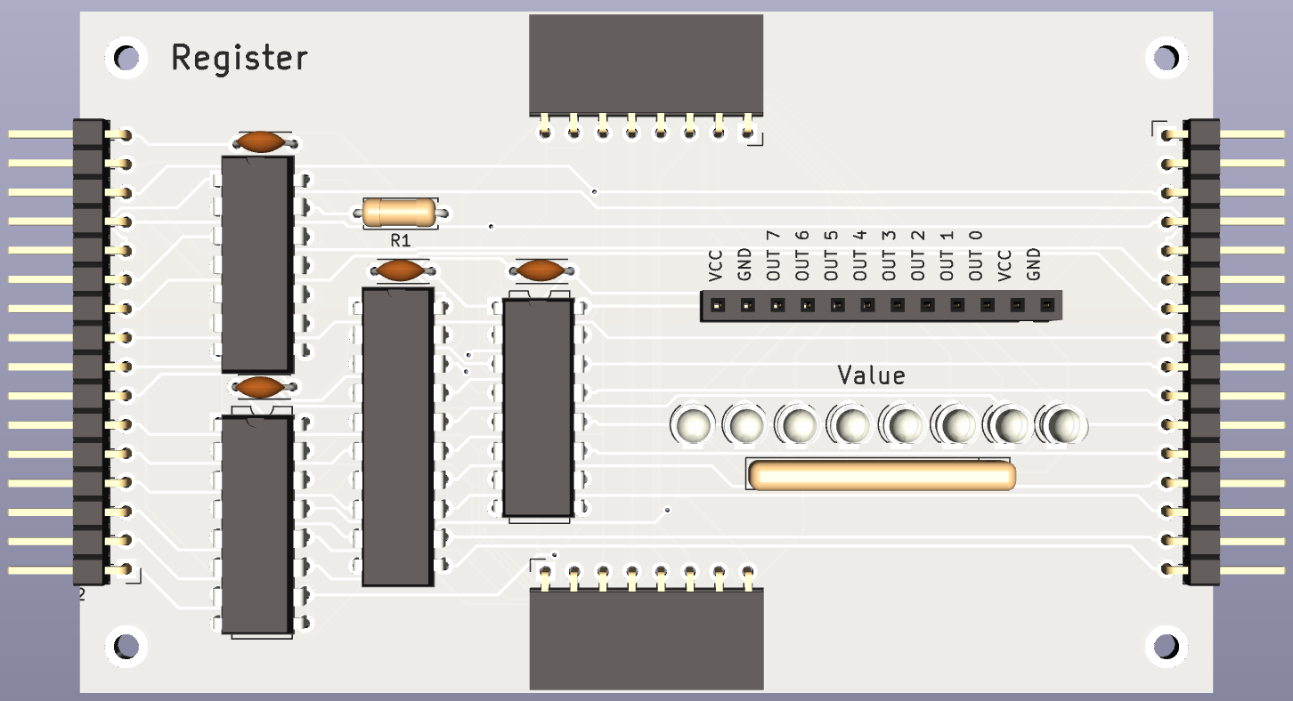
  • Register: Stores 8 bits, and can connect directly to an adjacent board above or below to expose its value (for use by the ALU and shift / rotate module). Has output headers, to interface with peripherals.
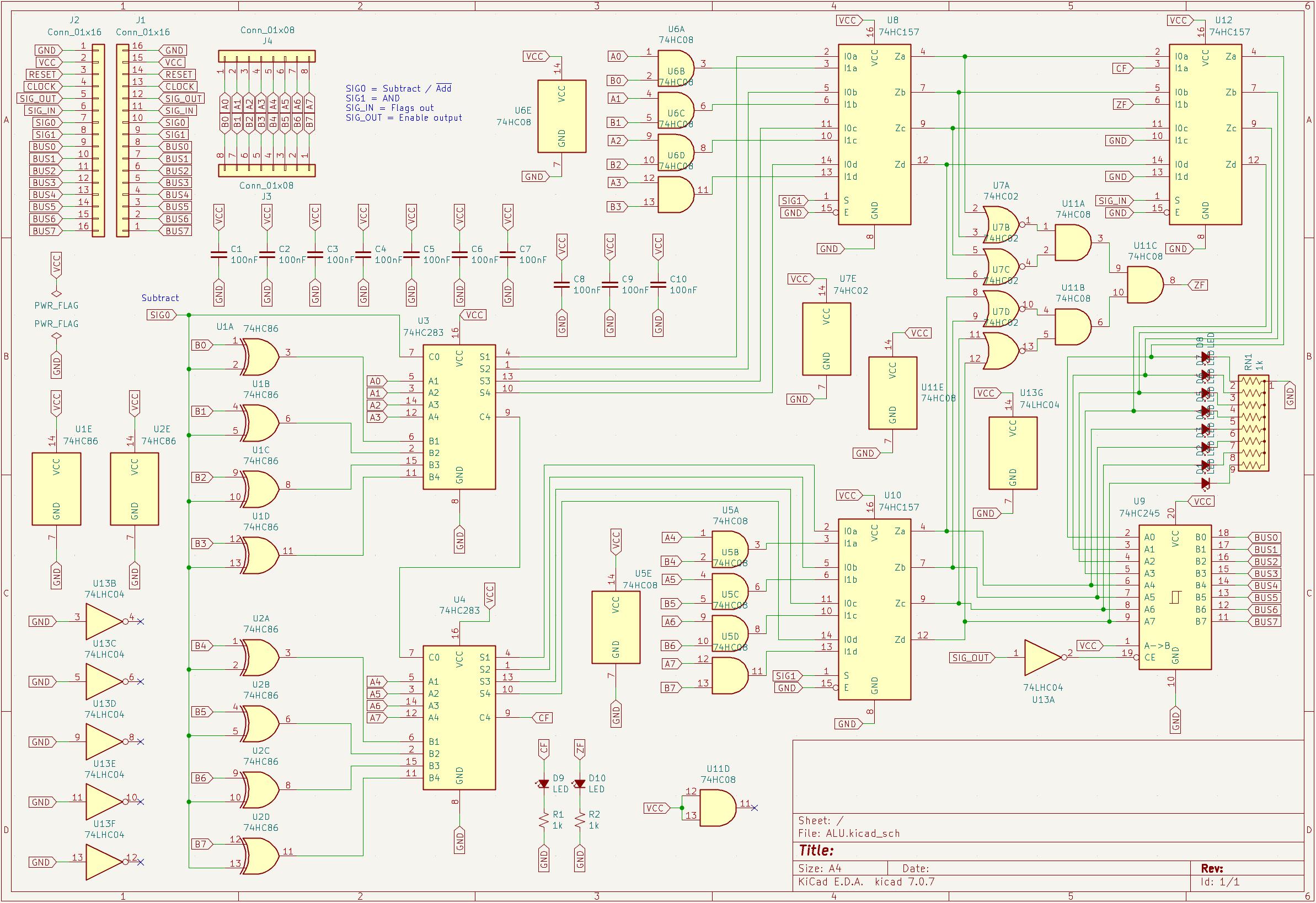
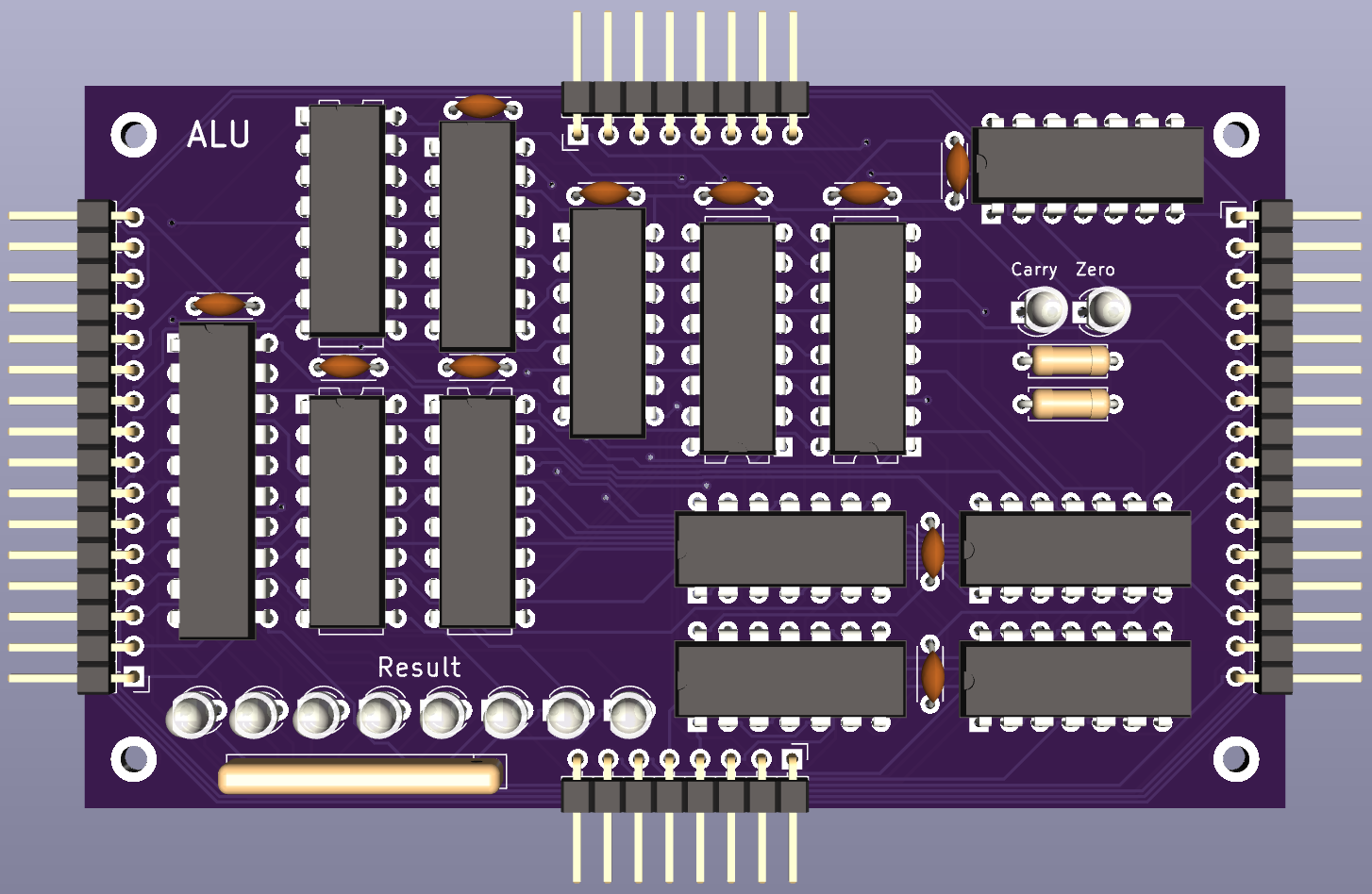
  • ALU: Performes calculations on values from register modules above and below it. Can output: add, subtract, bit-wise AND, or the carry-bit and zero-flag for any of those operations. Must be placed in the 1111 position (bottom right of top-most bus board), because the control module is hard-wired to input to the flags register when the read signal to that module position is enabled, which also enables flag output on the ALU.
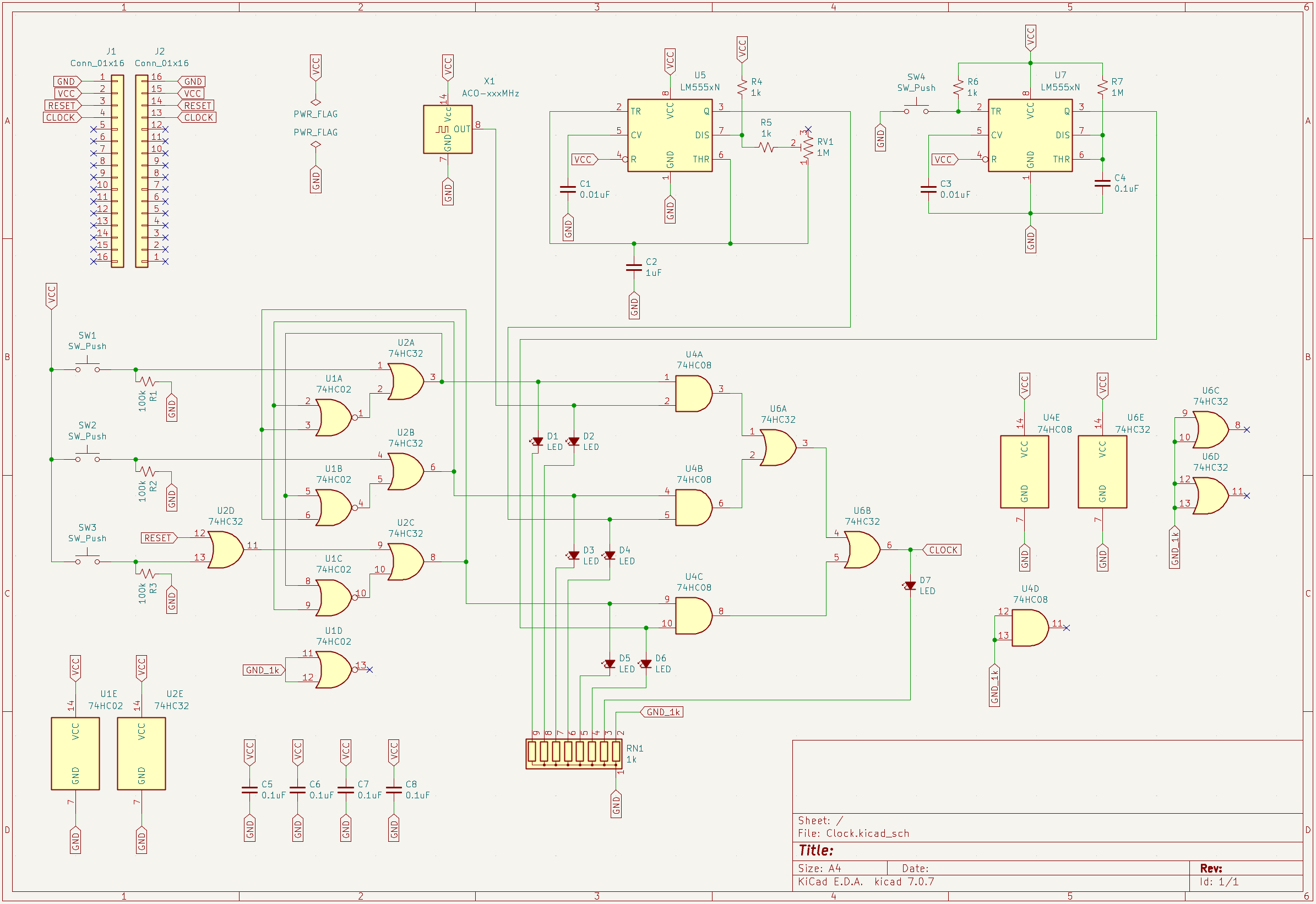
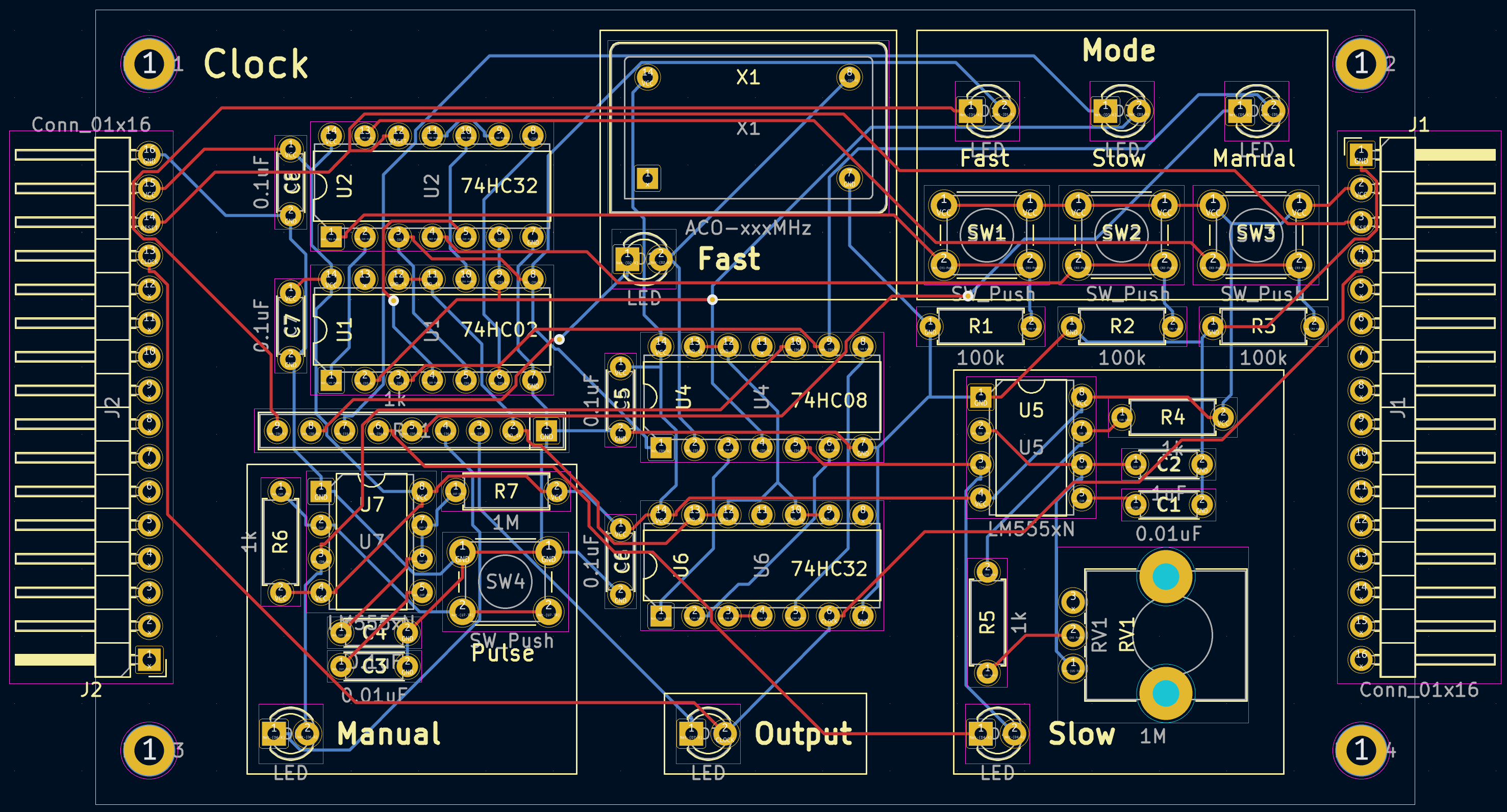
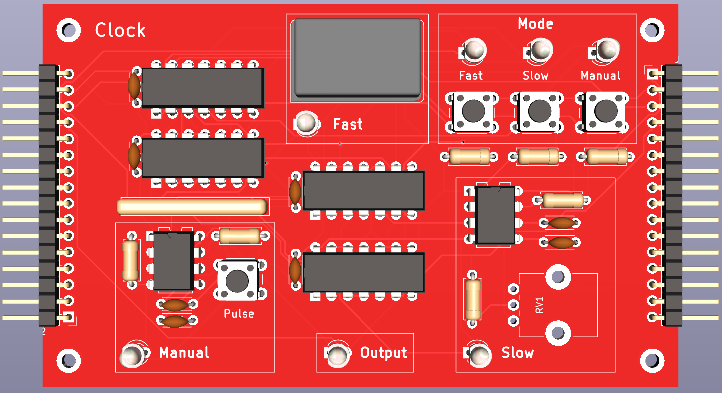
  • Clock: Provides the clock pulse for the computer. Has three modes: manual with button to pulse, 555-timer with potentiometer to adjust timing, or crystal oscillator (2MHz seems to work).
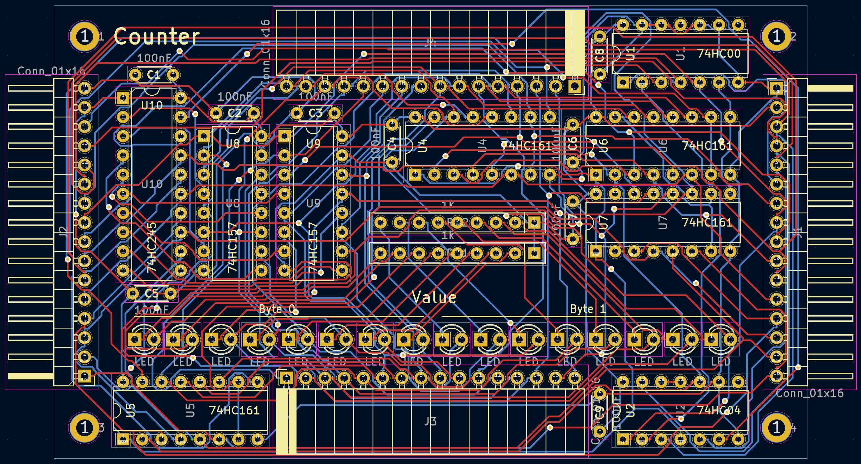
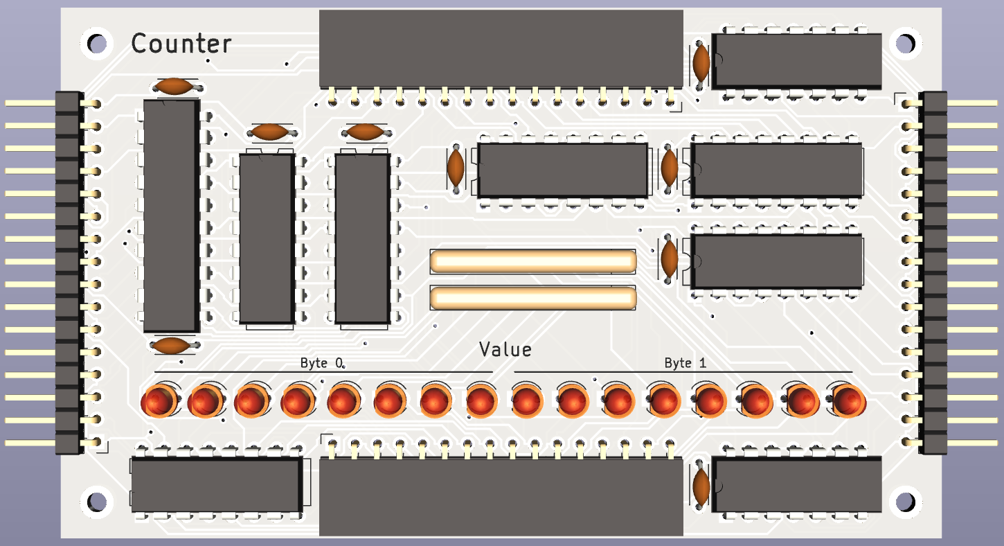
  • Counter: Stores and counts 16-bit values. Uses two global signal lines to select which byte to read / write, and whether to enable counting. Used for both the RAM address register and program counter / program memory address register.
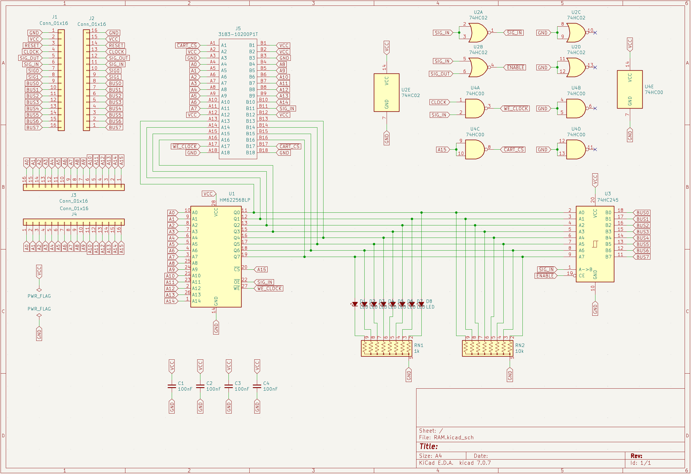
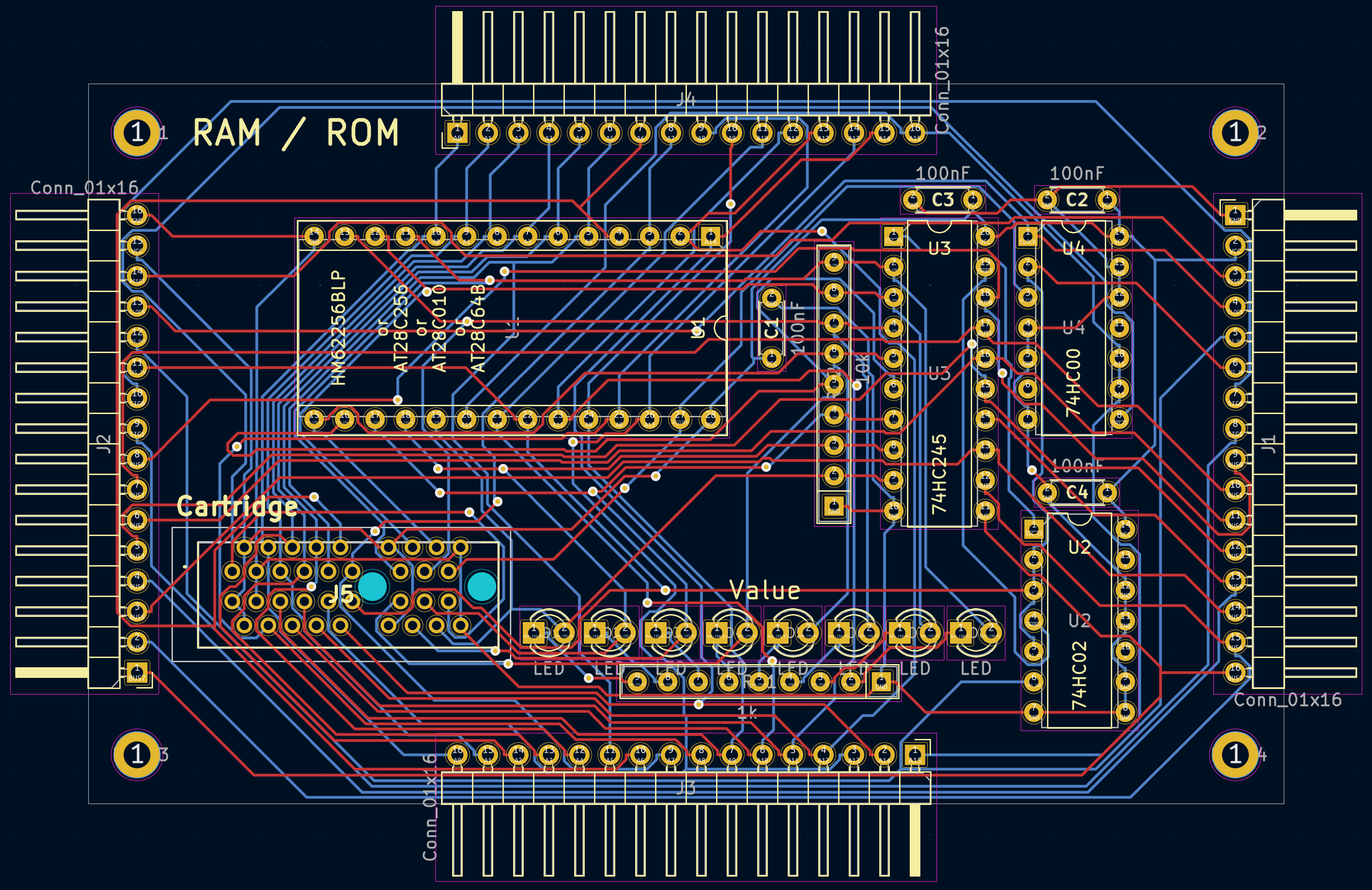
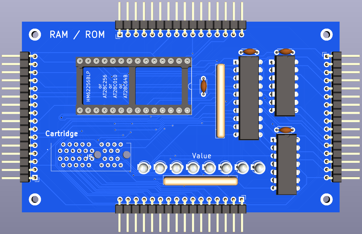
  • RAM: RAM or EEPROM (they have the same pinout). Used for the program memory EEPROM (not intended to be written to), and the static memory used for storing data. Up to 15-bits of address are taken from an adjacent counter module. Also has a cartridge slot, and switches between it and the EEPROM on the board using the 16th address bit. This allows swapping out programs much easier
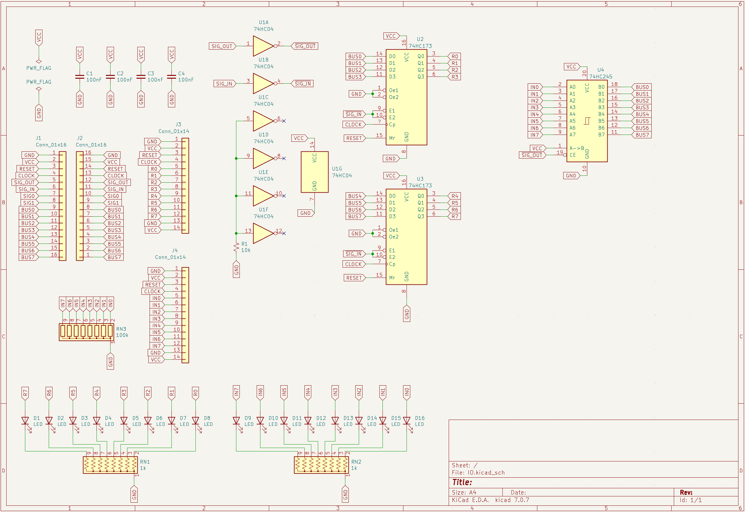
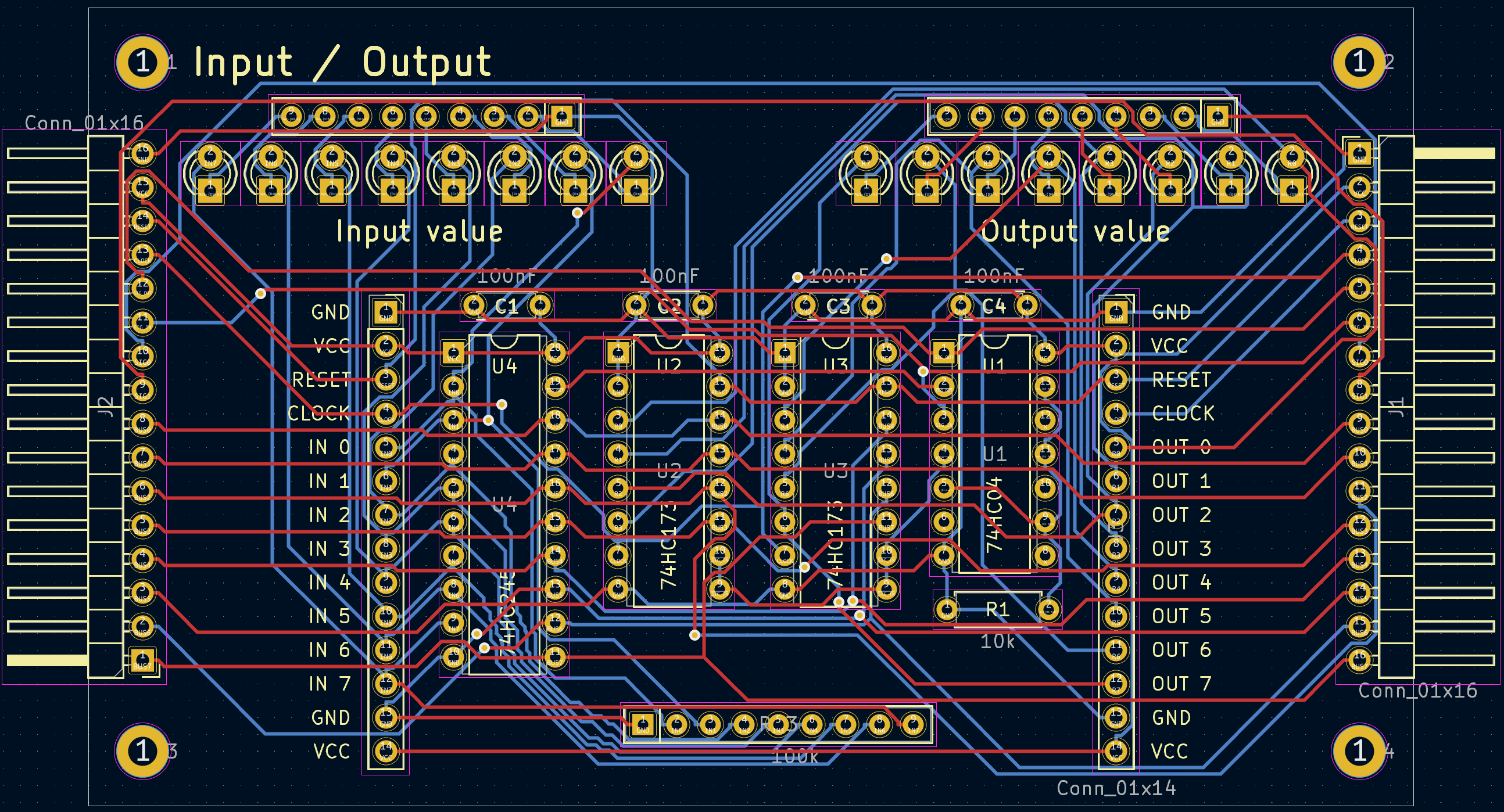
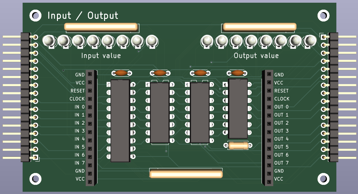
  • Input / Output: Like a register module, except when outputting to the bus, outputs the value from input headers instead of the registers. The 8-bit value stored in the registers is accessible on output headers as well. The two headers are in parallel, making it sturdy to plug in a peripheral that uses both.
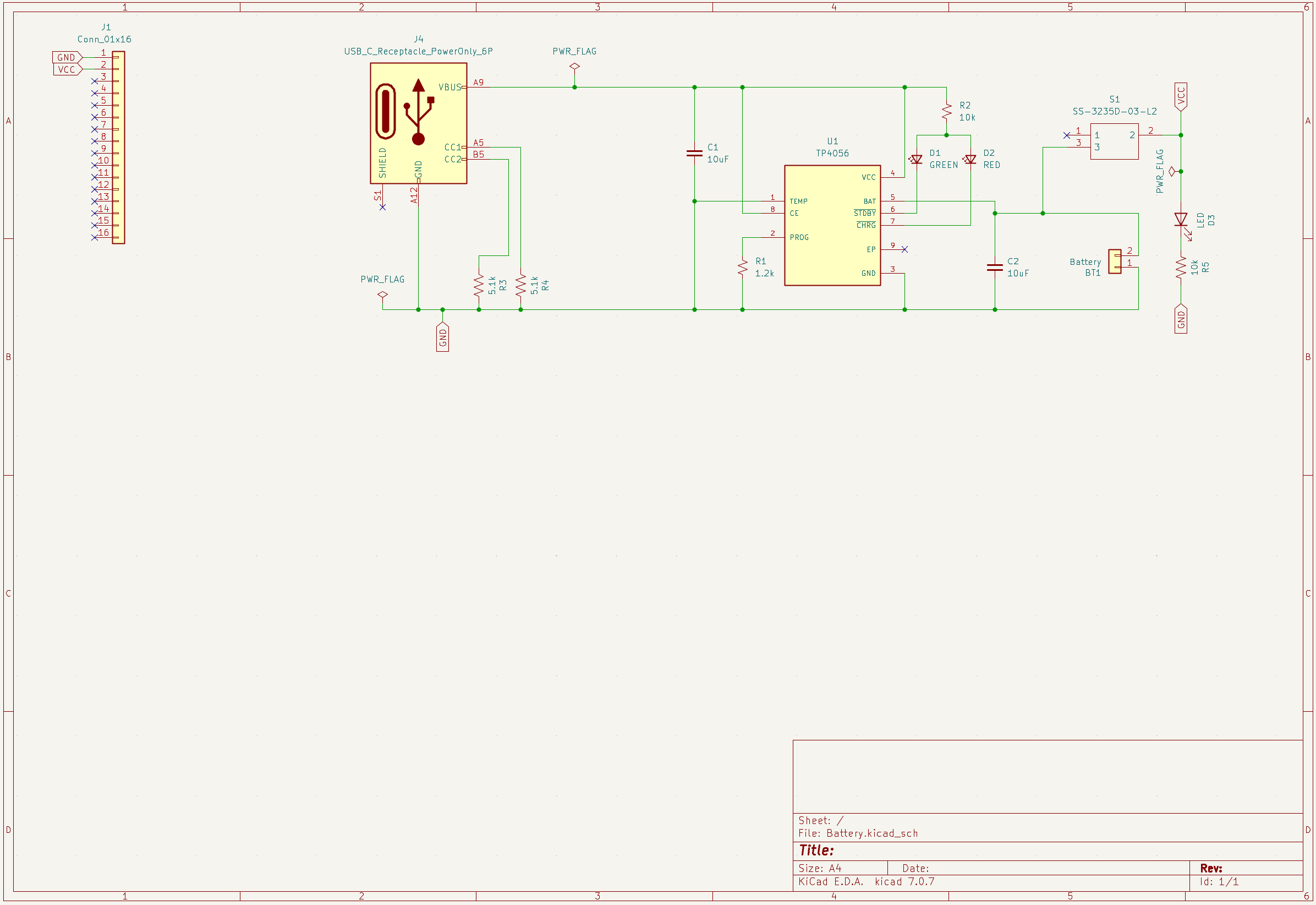
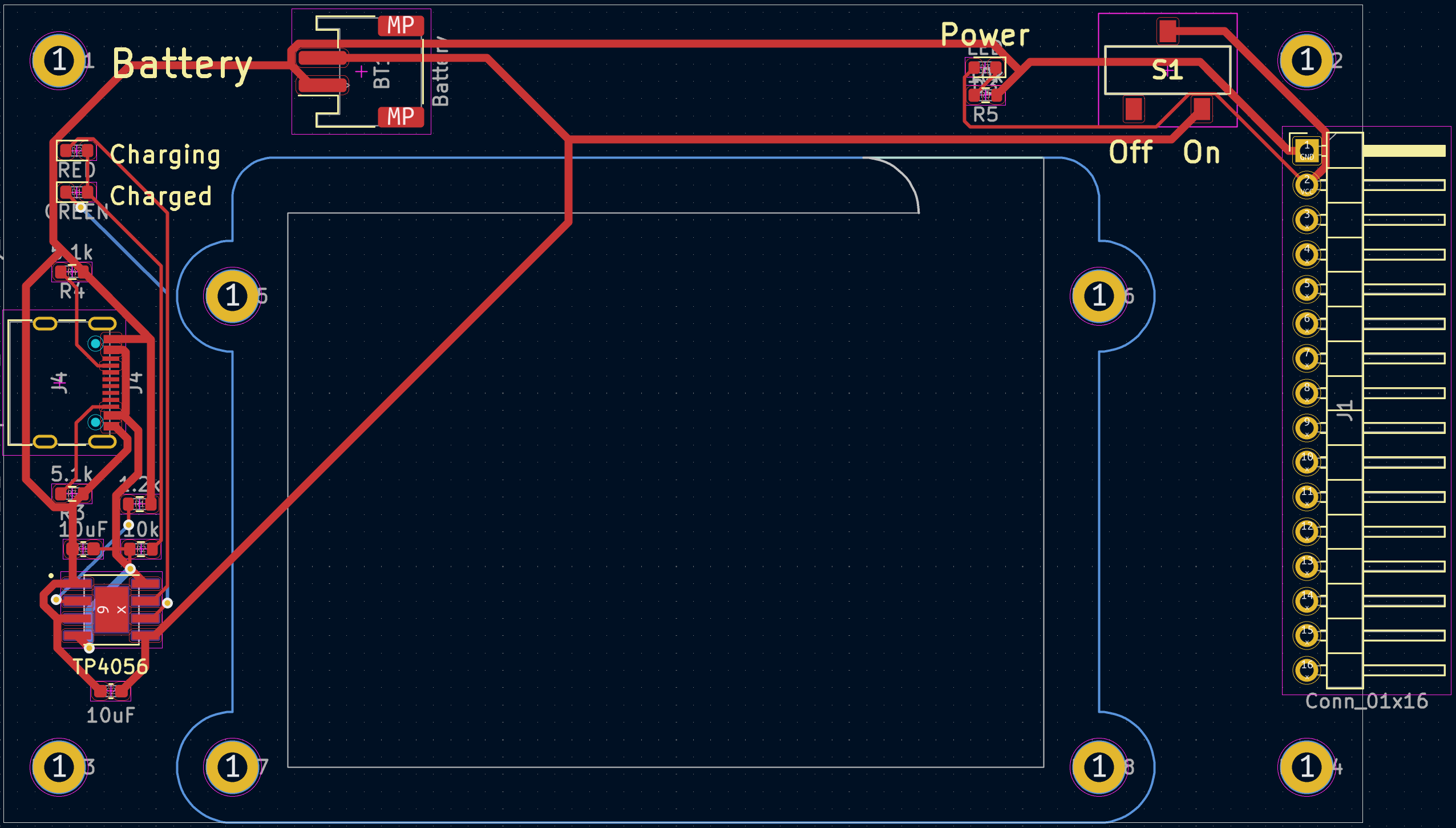
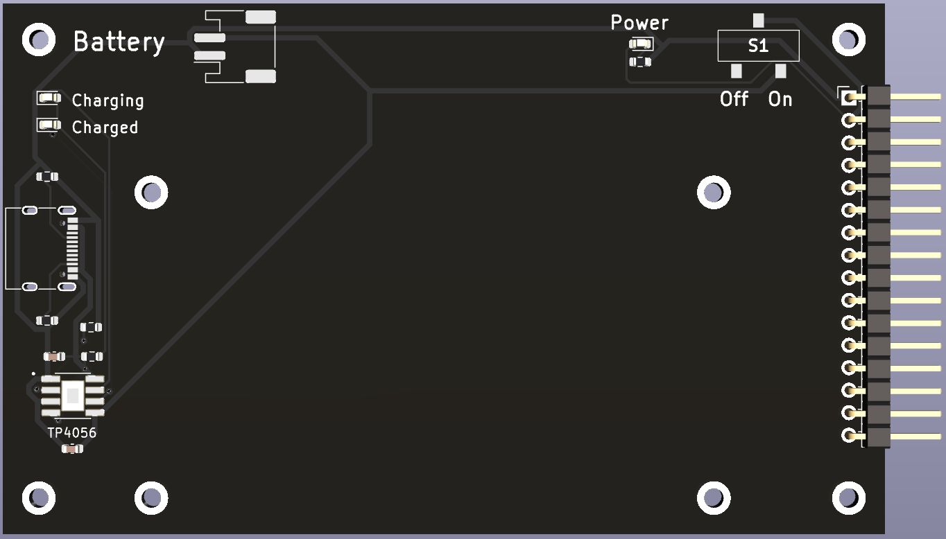
  • Battery: Has a battery, charging capability with USB-C, and a switch to output power to the CPU.

Layout

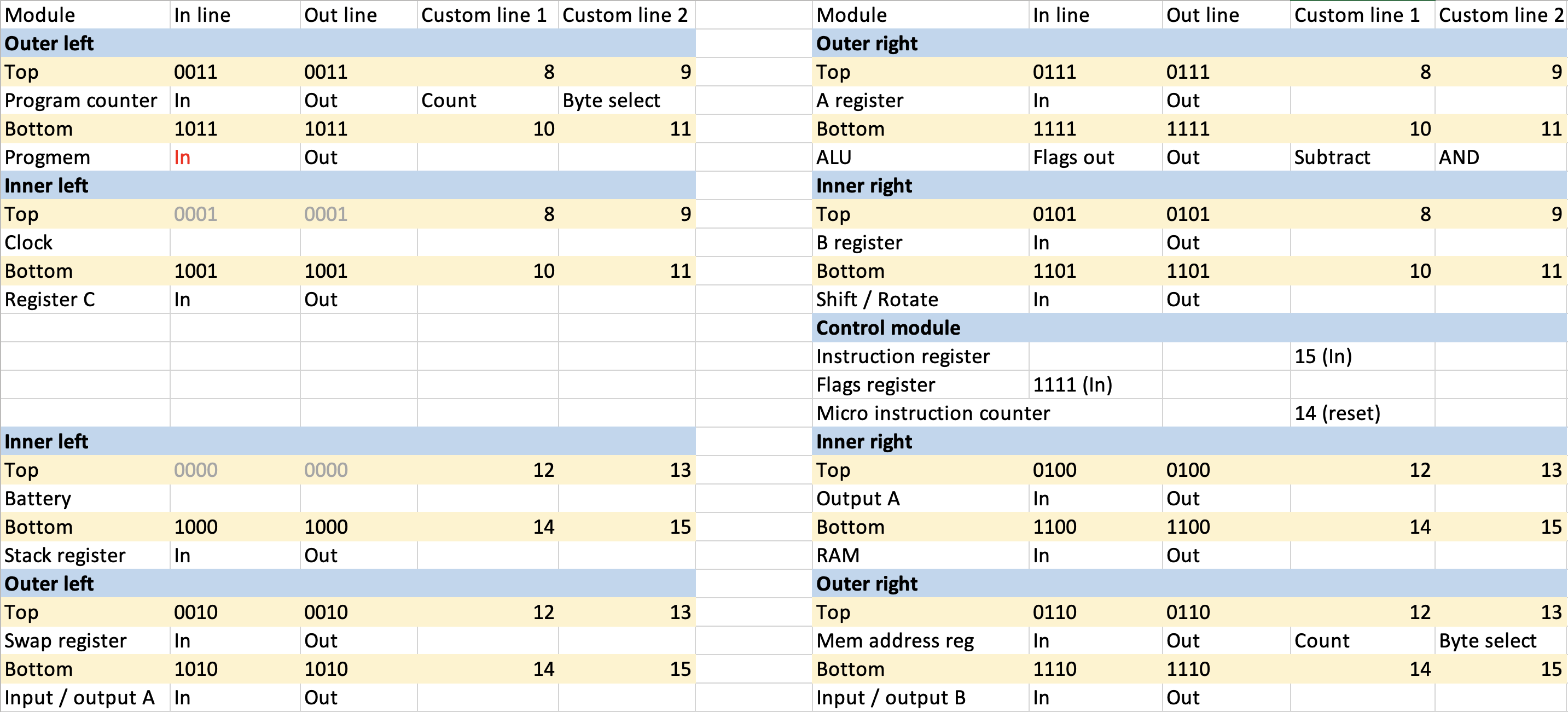
In general, any of the 16 module slots can input from or output to the bus, so most modules could go in any position. However, some of them have to go in specific slots, because:

  1. The 0th slot on the top and bottom aren't usable for in/out selection, because it's ambiguous whether that slot is selected or if no module on that side is selected. The battery and clock go in those slots, since they only output power and a clock signal, and don't use the bus.
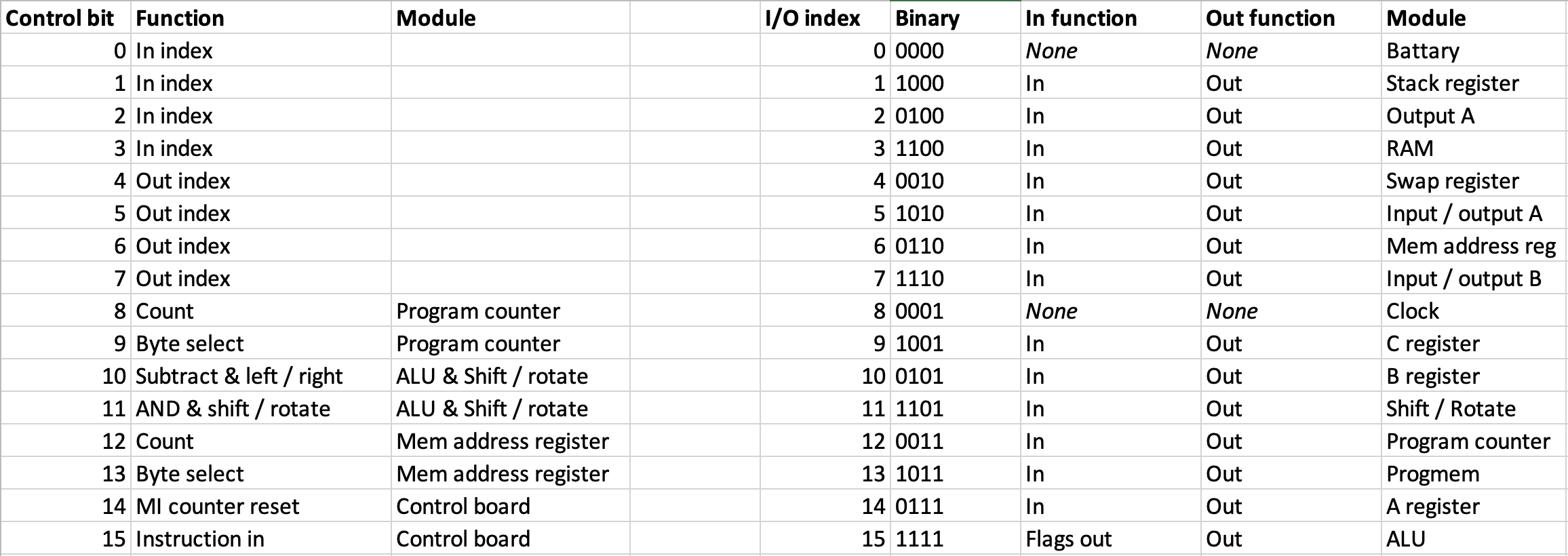
  2. The 8 "custom" signals (that mean something different for different modules) are split up into 4 for top, 4 for bottom. Those 4 are split into pairs; the top 2 modules on each bus board get one pair, and the bottom two get the second pair. The second pair of signals on the bottom is actually used by the control board.
  3. Some modules (RAM / ROM, ALU, and Shift) get inputs from other modules, so their inputs have to be next to them.

Top left: The program counter goes in the top to use the first pair of custom signals (for count and byte select), plugging into the program memory below it. Below that is the clock (in the 0th position), and Register C.

Top right: The ALU goes one slot down from the top, to use the second pair of custom signals (for add/subtract and bit-wise AND), with register A and B as its operands above and below. Then the shift / rotate module goes at the bottom plugging into register B. These need to be on the right side to avoid the 0th position. The shift module shares custom signals with the ALU, which is okay because only one is used at a time, and the signals don't have an effect if that module isn't outputting.

Bottom left: The battery takes the top 0th slot, and then the stack and swap registers, and input / output A module after that. Other than the battery, the positions are arbitrary.

Bottom right: The output A register goes at the top and the RAM goes below it. The memory address register goes in the next position to get the first pair of custom signals (for count and byte select), and plugs into the RAM above it. The input / output B module goes at the bottom. The memory address could instead go where output A is, and RAM just needs to be next to it. The other two could go anywhere.

Peripherals

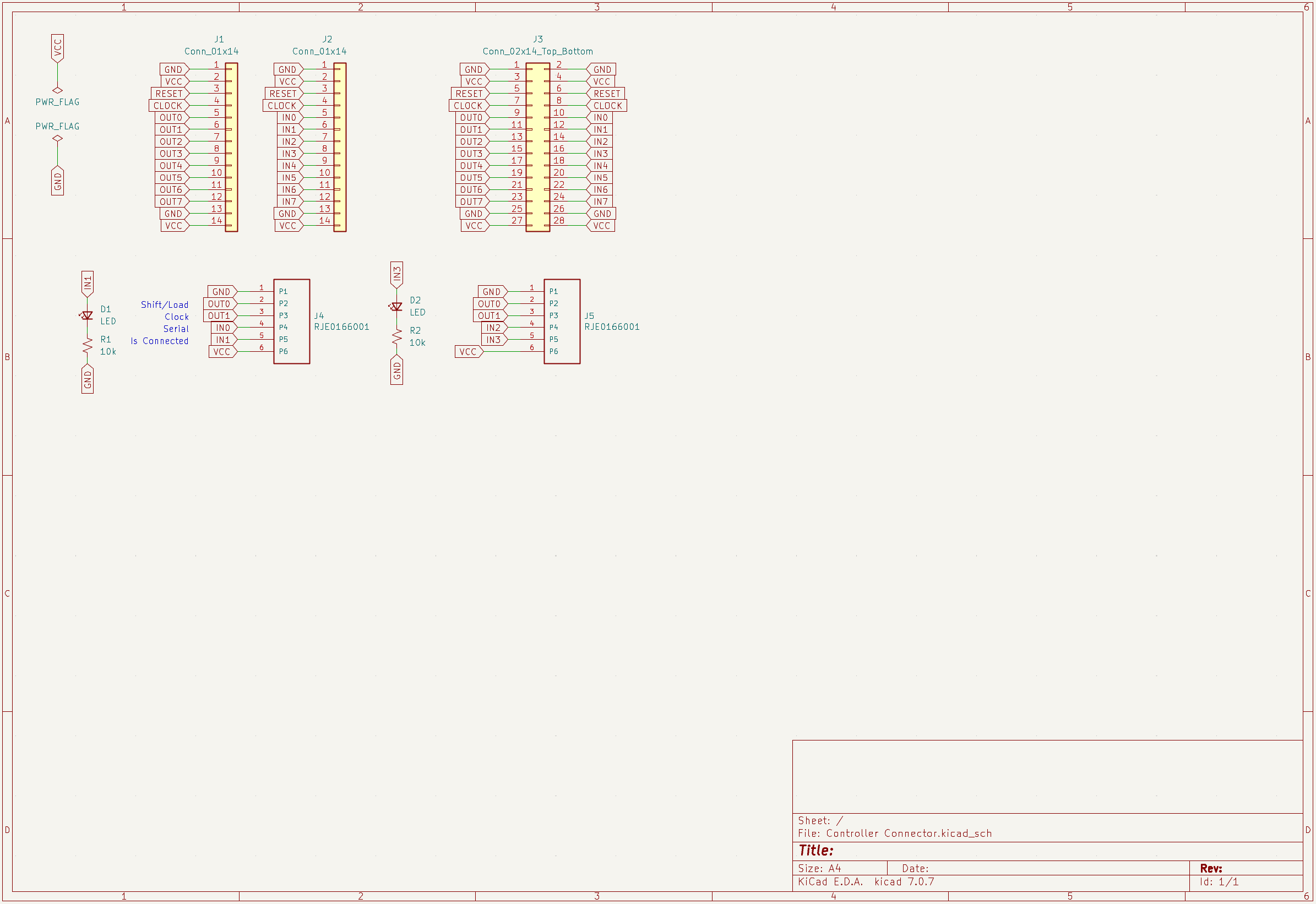
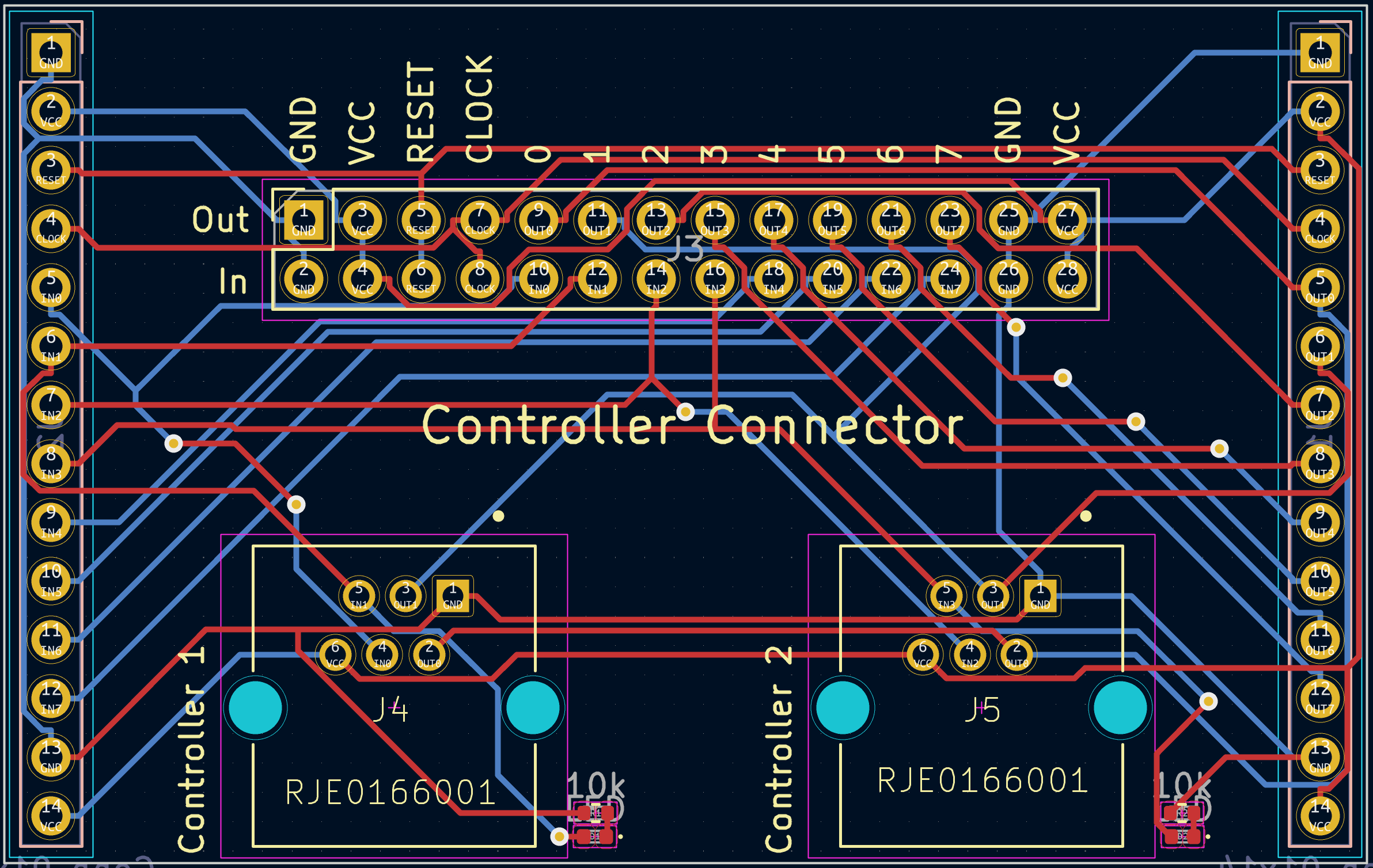
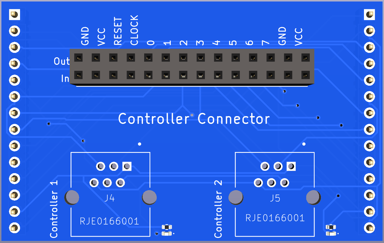
  • Controller Connector: Plugs into IO module, and has two RJ12 plugs on it, to connect to parallel-to-serial shift register-based controllers.
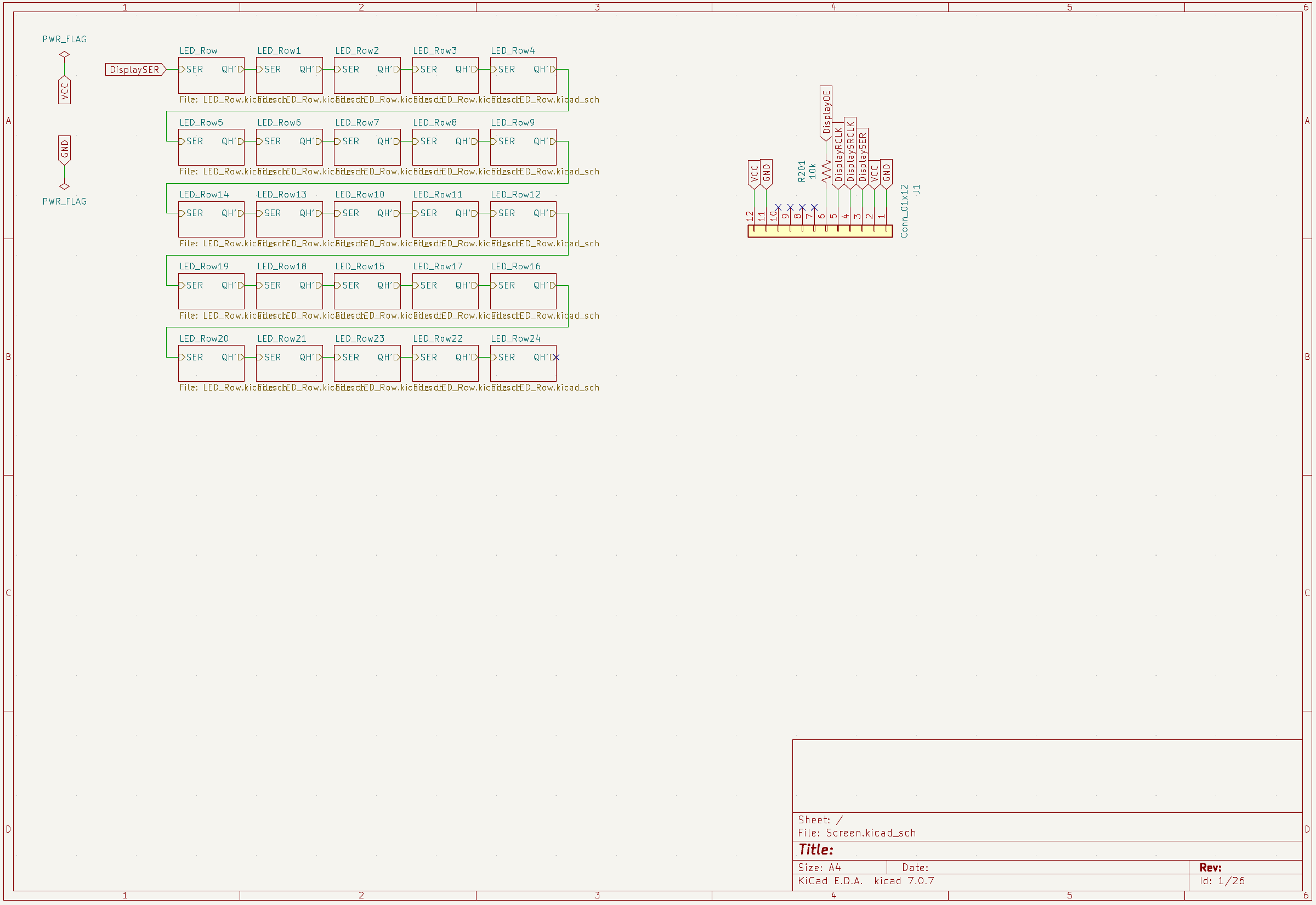
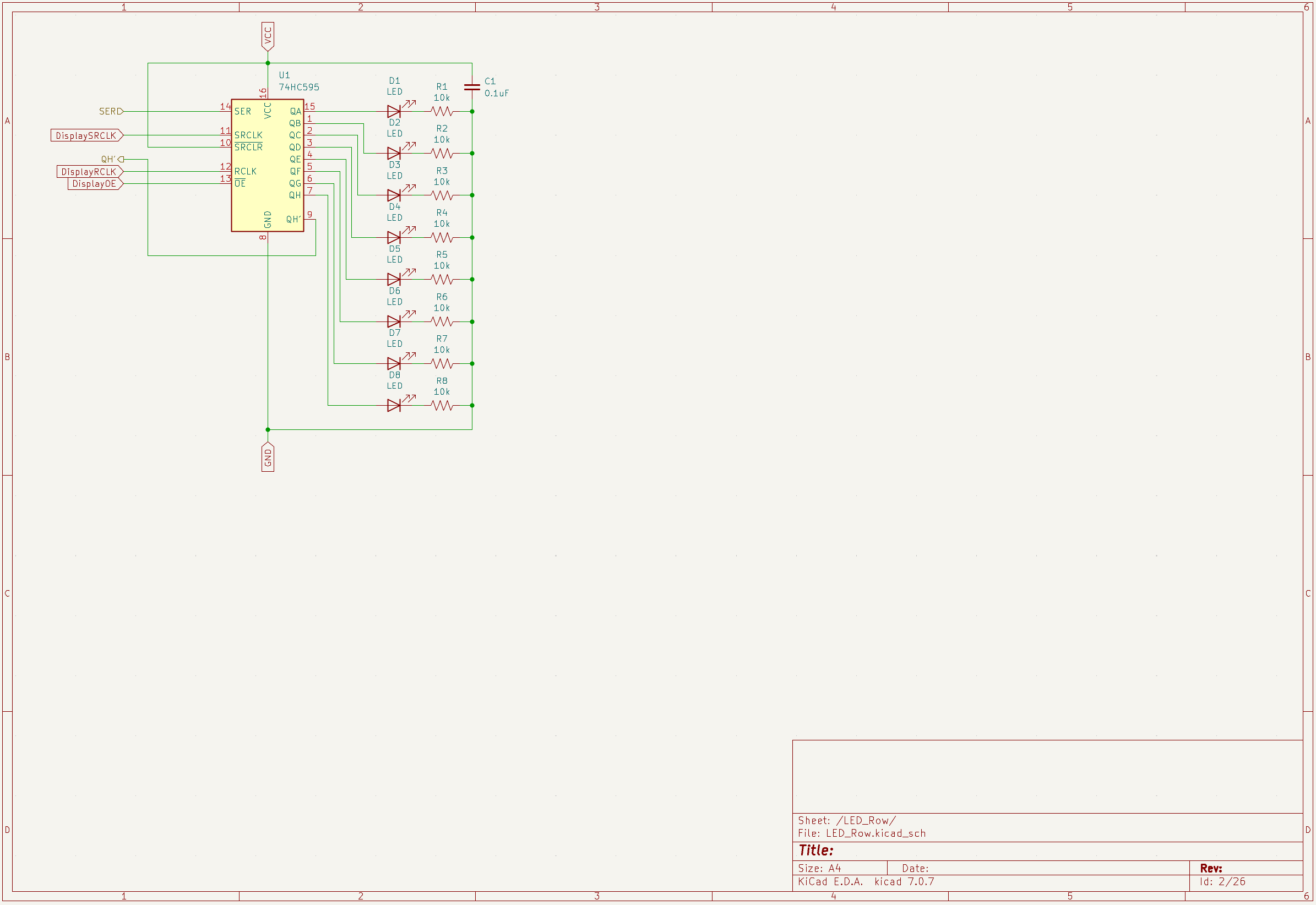
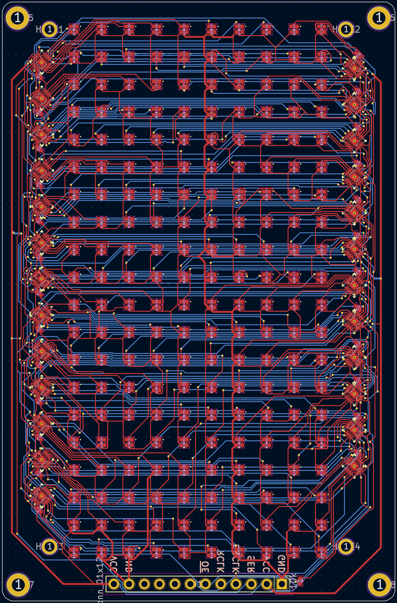
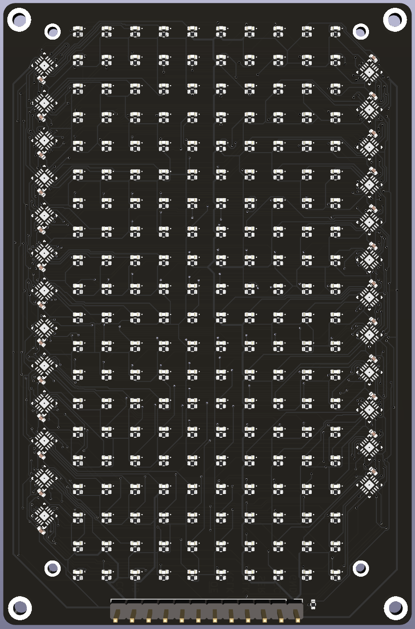
  • Screen: An 10x20 595-shift register-based monochrome display. Plugs into output module (vertically), or IO module (horizontally).
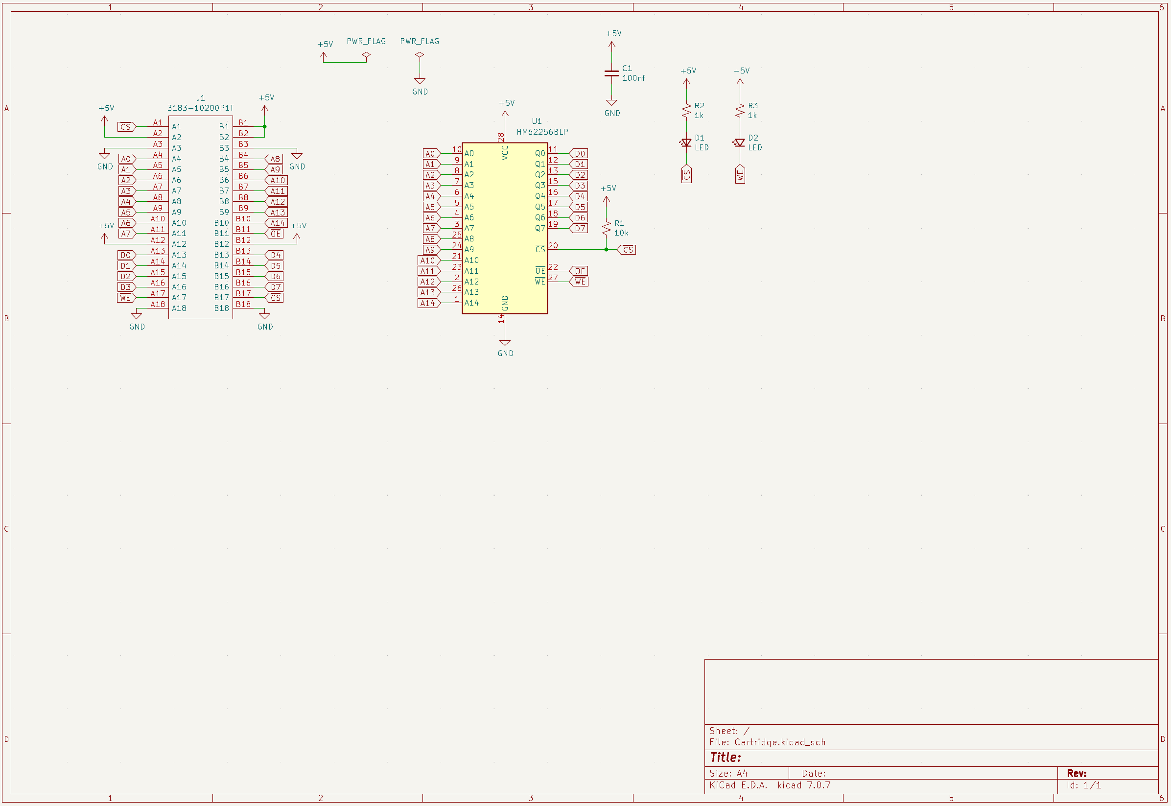
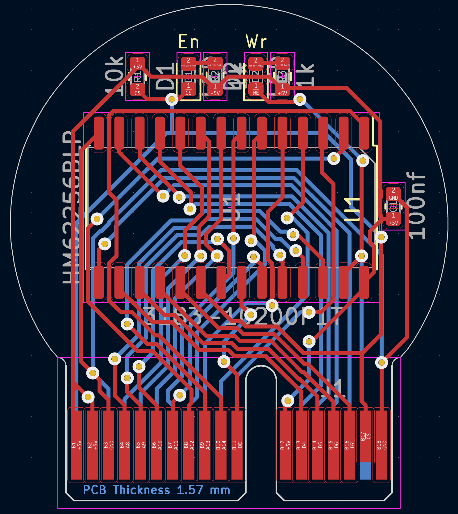
  • Cartridge: A small board with a surface-mount version of the same 28C256 EEPROM used as in the program memory module. Plugs into the program memory module with the smallest PCIe board edge connector.
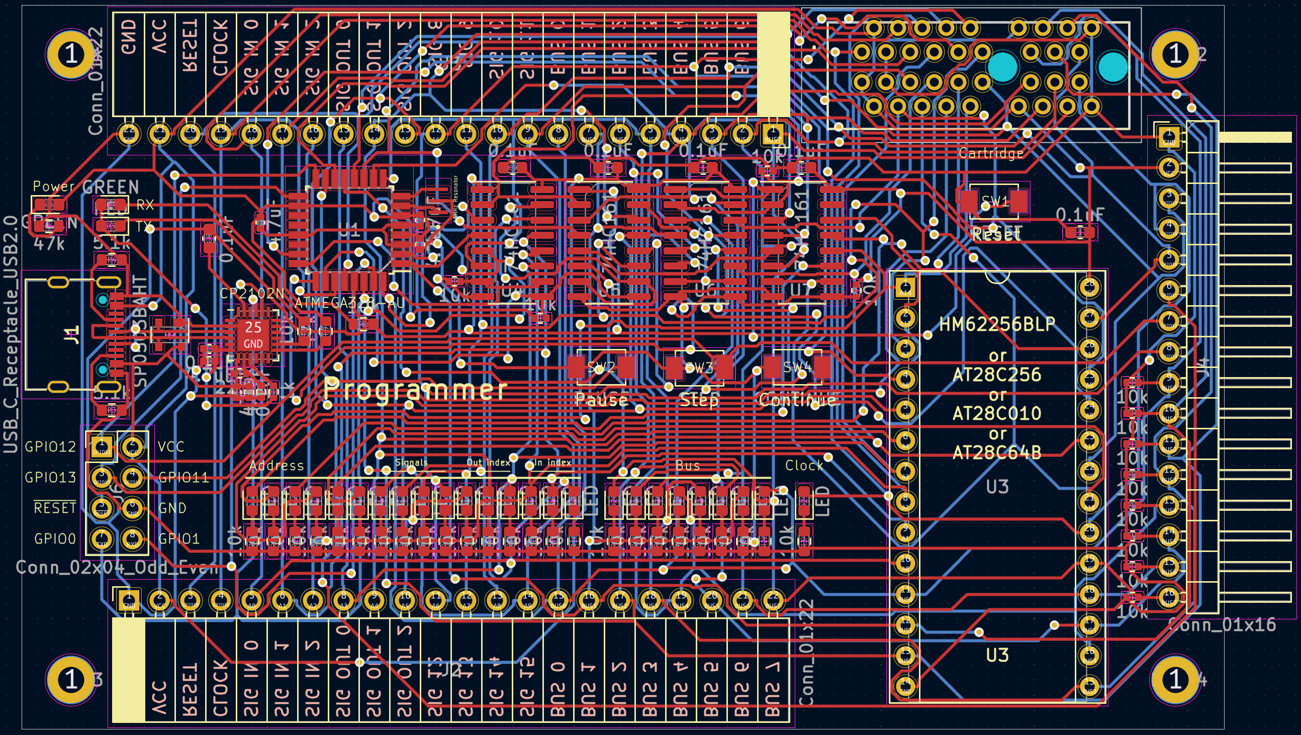
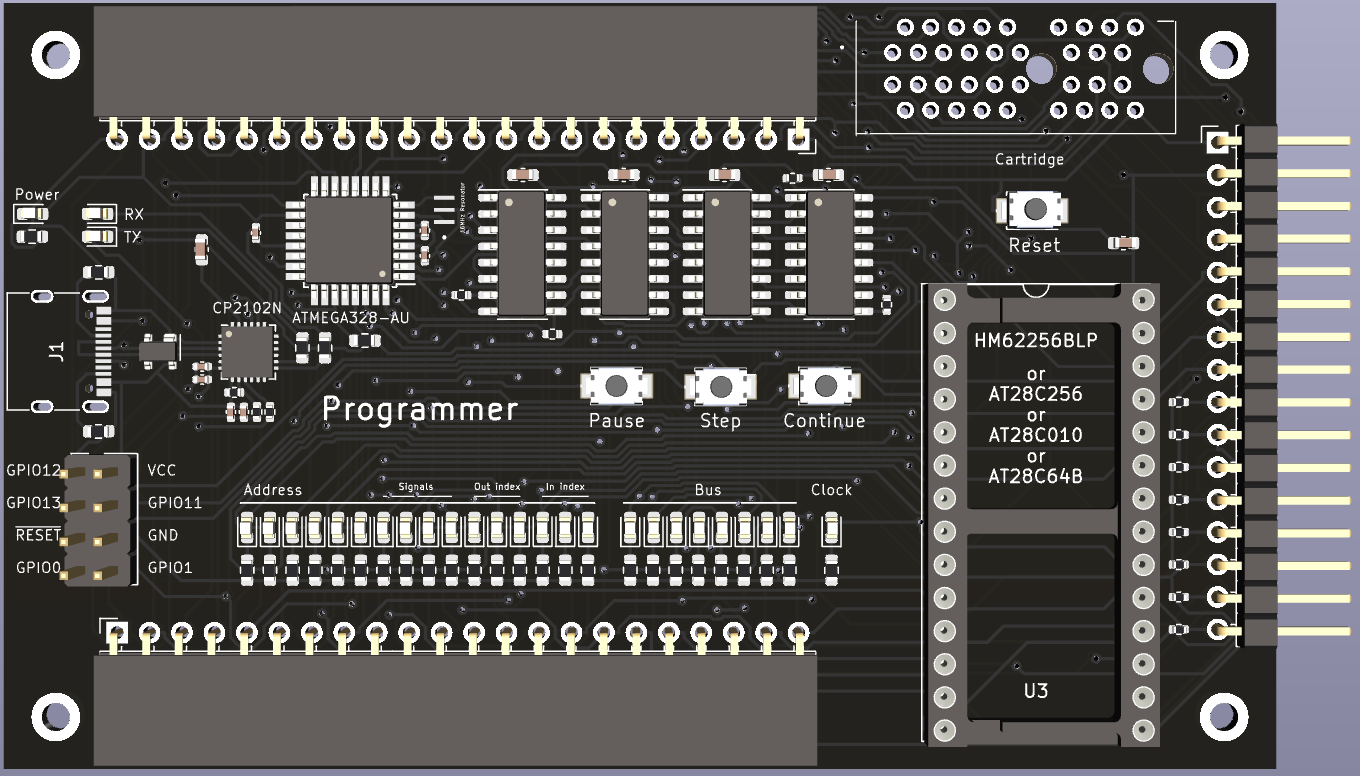
  • Programmer: Arduino-based board used to program and test the CPU in 3 ways:
    1. Separate from the CPU, read / write to EEPROMs (big ones, or cartridges).
    2. Plug into bus boards, to test all the modules plugged in (doesn't work, because the bus is needed to set the signals, but that could cause bus contention).
    3. Replace the program memory and clock, to have a very fast development cycle to write program code (not necessary now that there's an emulator), or to test the CPU.

Layout, signals, and parts list

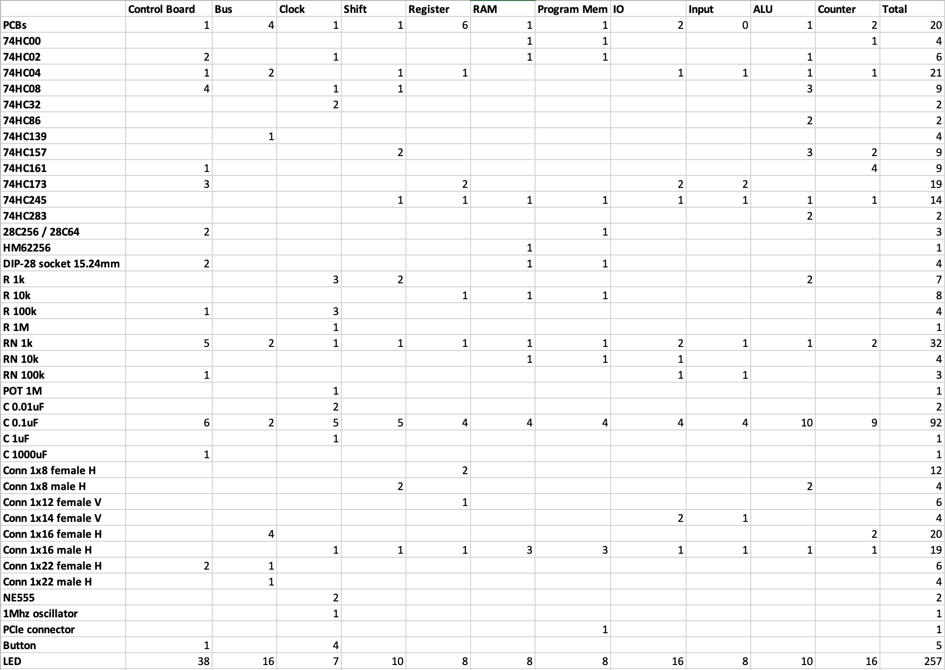
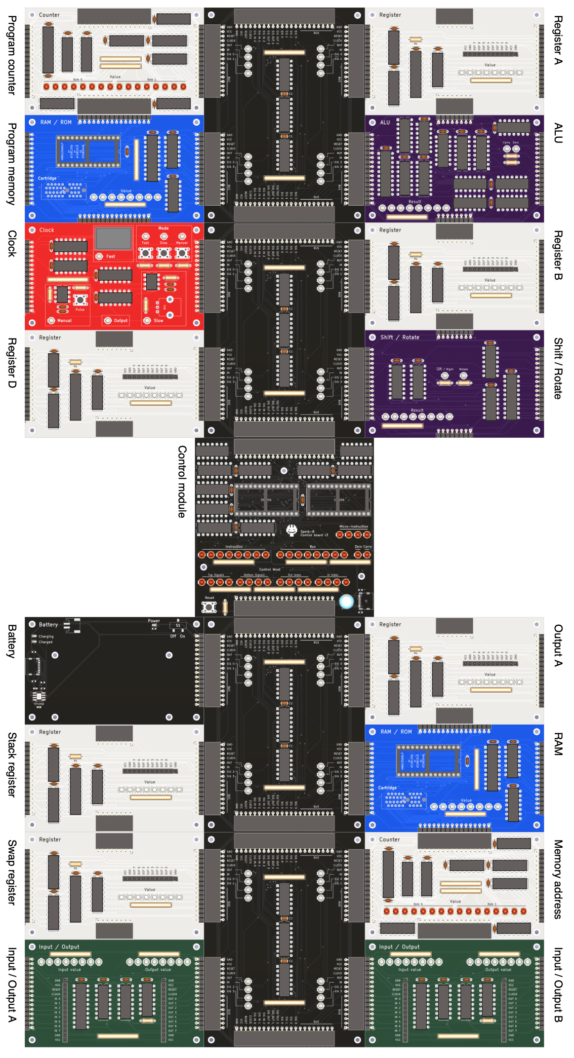
These images show the layout of the modules in the 16 slots, the functions of each of the signals, and a parts list. Module layout Signal functions Parts list

Design images

Overall layout

Layout of the CPU

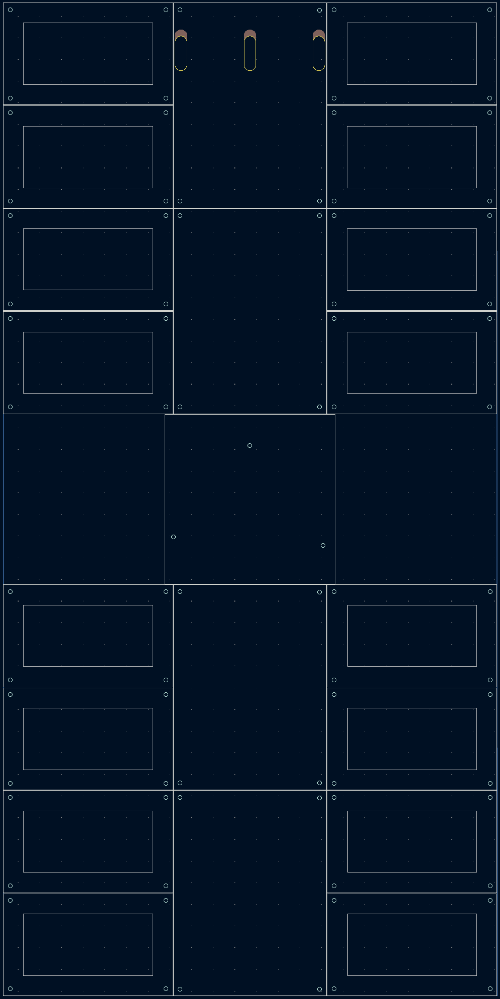
Mounting board (laser cut acrylic)

Mounting board design

Schematics

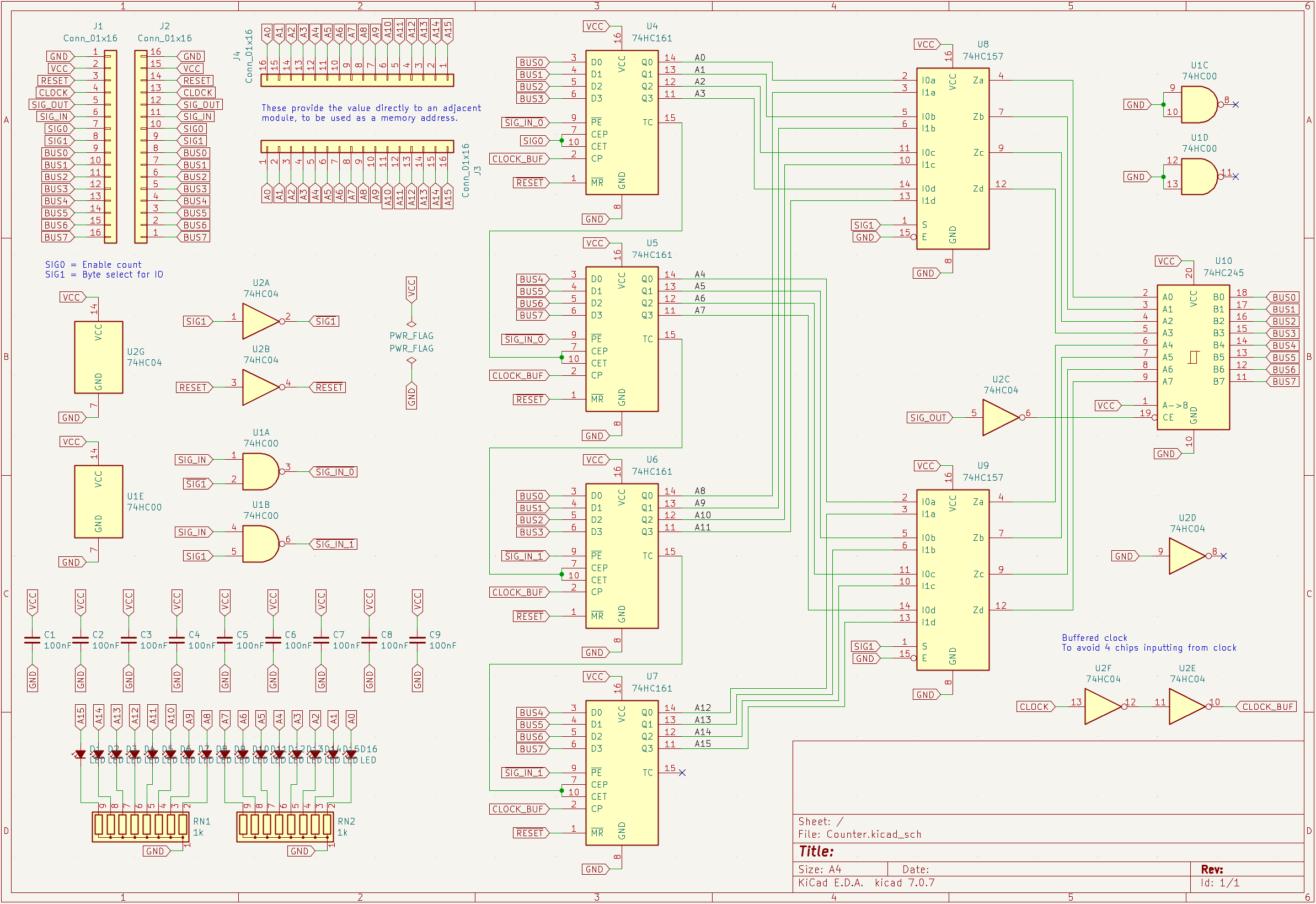
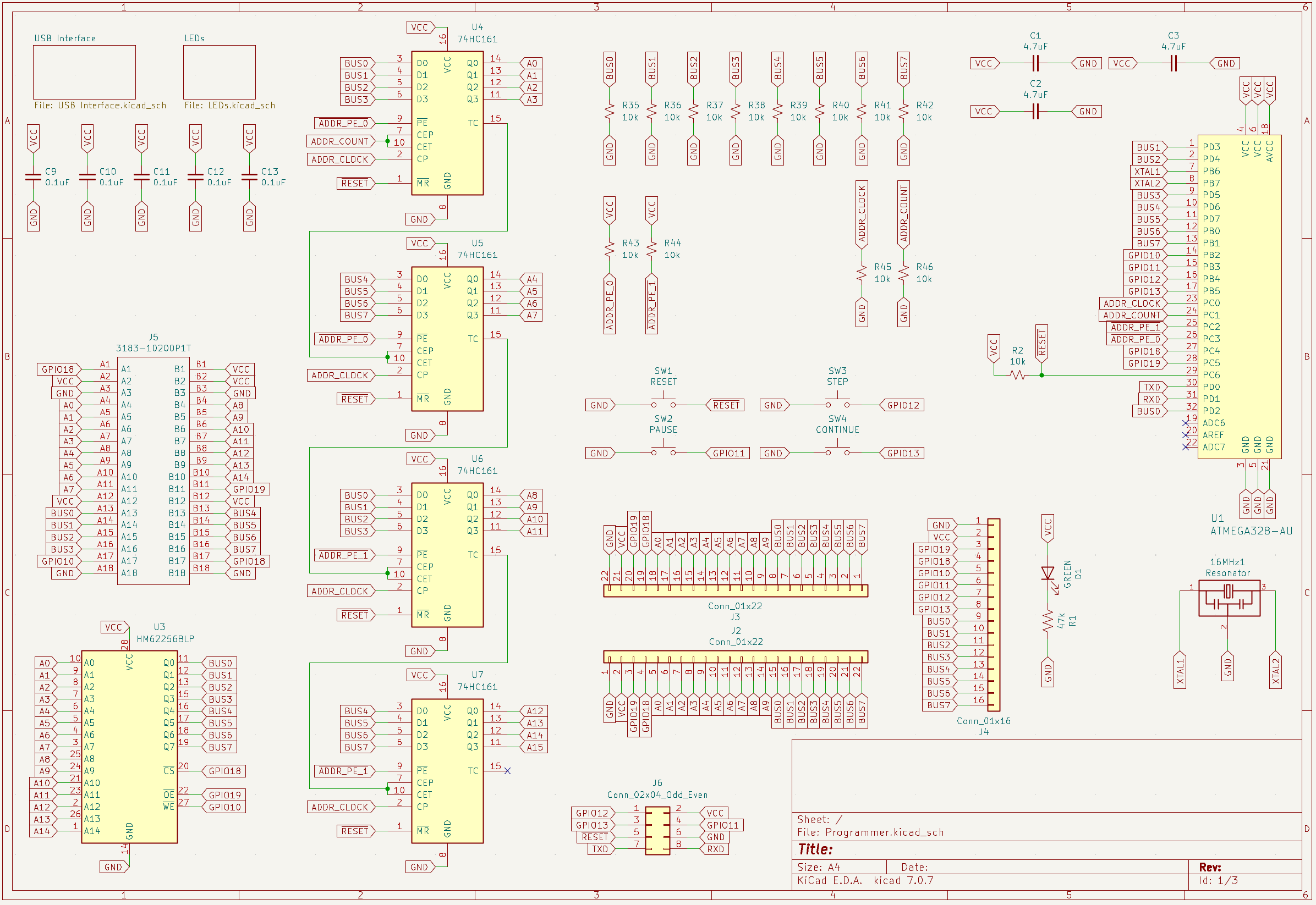
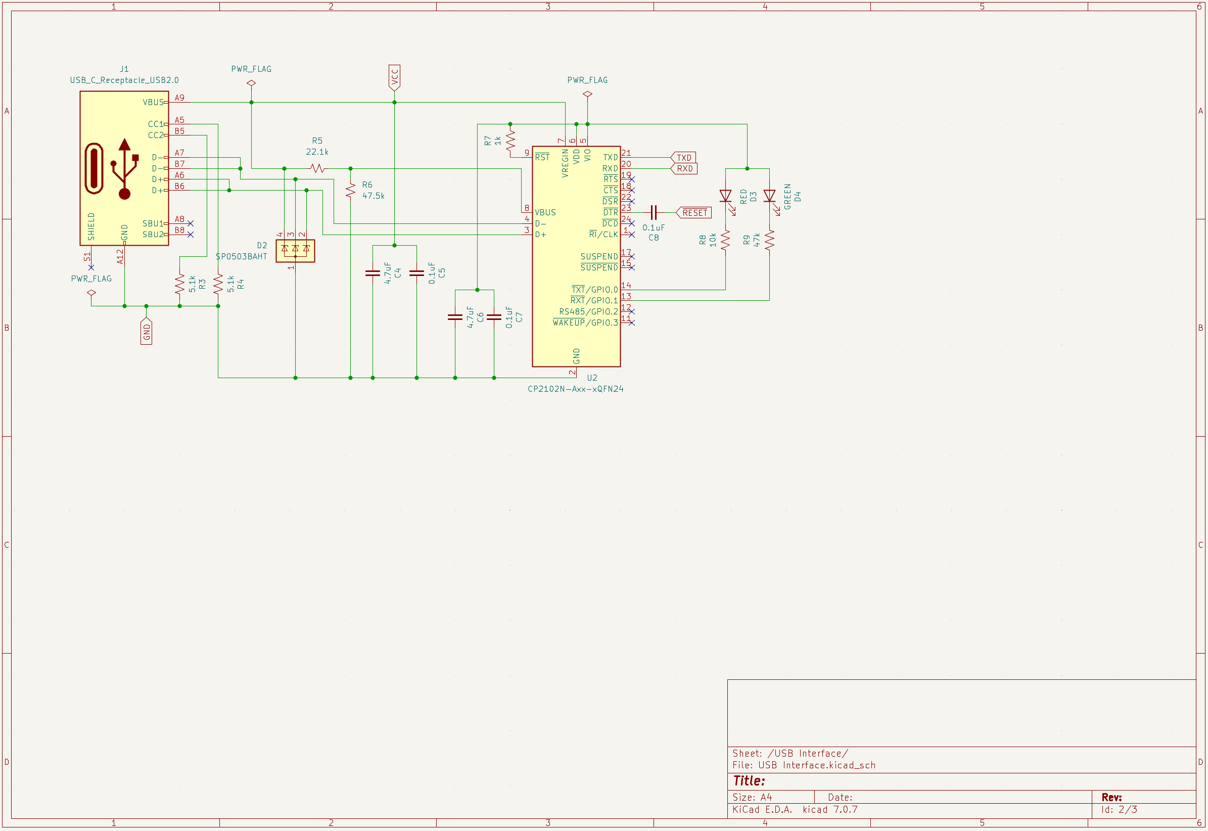
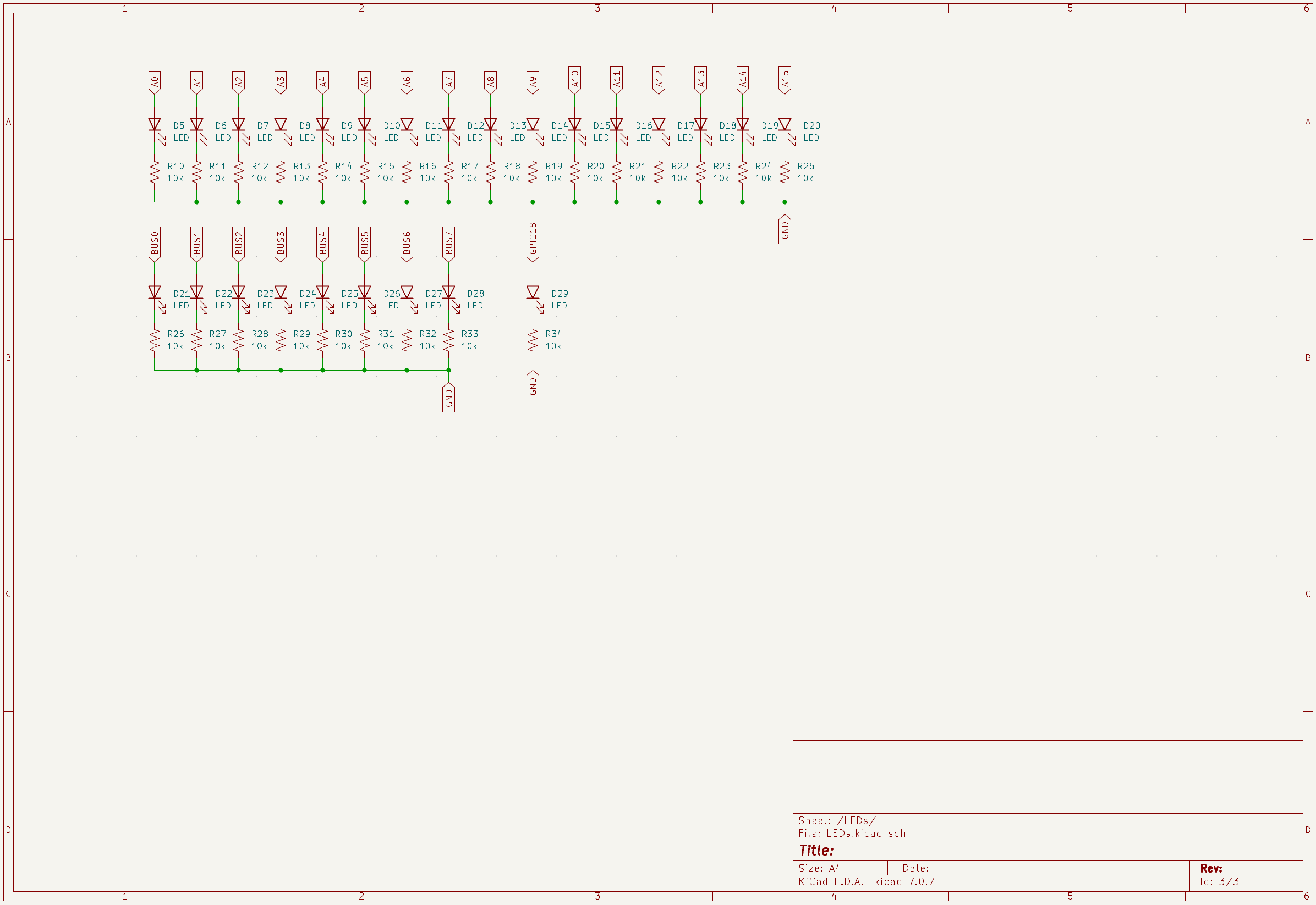
Control Module schematic Control Module bus interface schematic Bus schematic Register schematic ALU schematic Shift / Rotate schematic Clock schematic Counter schematic RAM schematic Input / Output schematic Battery schematic Screen schematic Screen schematic Controller Connector schematic Cartridge schematic Programmer schematic Programmer USB Interface schematic Programmer LEDs schematic

PCB Layouts

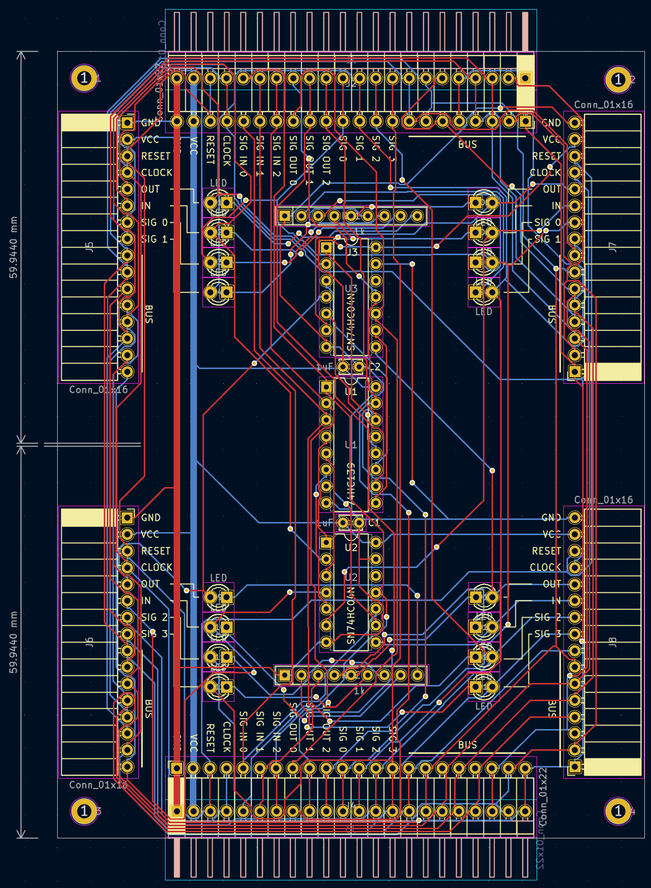
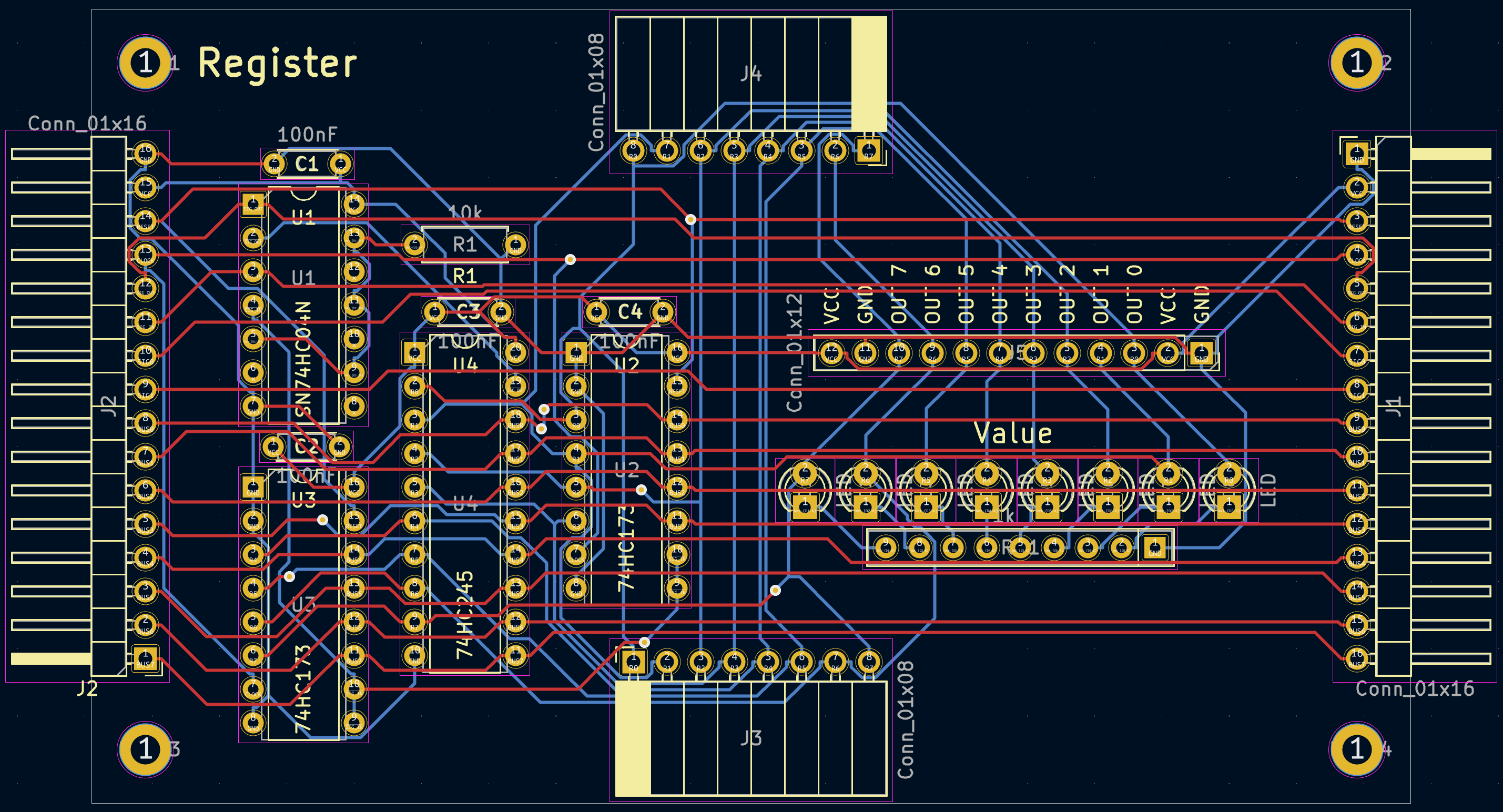
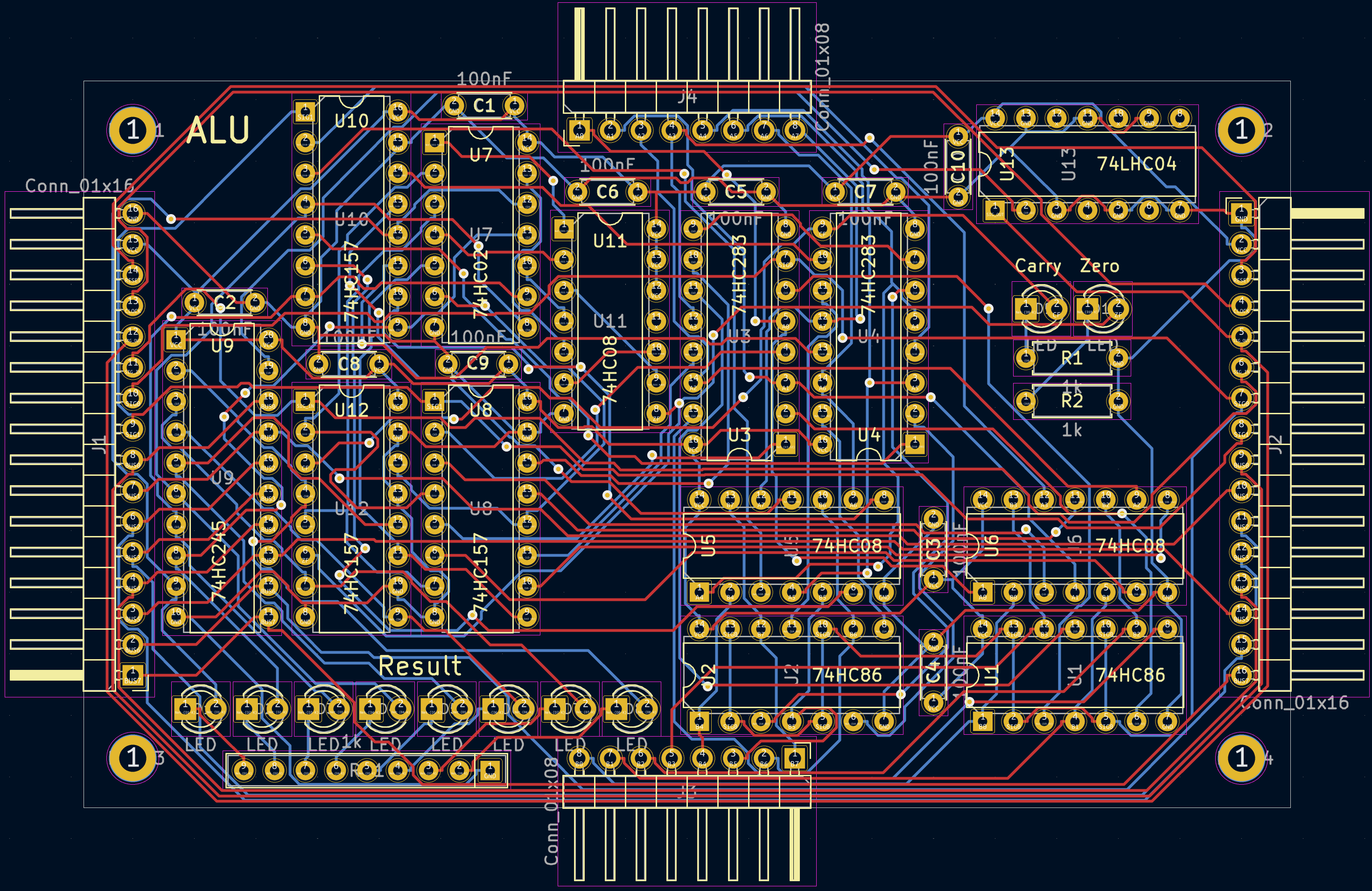
Control Module PCB layout Bus PCB layout Register PCB layout ALU PCB layout Shift / Rotate PCB layout Clock PCB layout Counter PCB layout RAM PCB layout Input / Output PCB layout Battery PCB layout Screen PCB layout Controller Connector PCB layout Cartridge PCB layout Programmer PCB layout

3D Renderings

Control Module 3D render Bus 3D render Register 3D render ALU 3D render Shift / Rotate 3D render Clock 3D render Counter 3D render RAM 3D render Input / Output 3D render Battery 3D render Screen 3D render Controller Connector 3D render Cartridge 3D render Programmer 3D render

Parts

31
QtyValueFootprintReferences
10LEDLED_THT:LED_D3.0mm_ClearD1, D2, D3, D4, D5, D6, D7, D8, D9, D10
5100nFCapacitor_THT:C_Disc_D4.3mm_W1.9mm_P5.00mmC1, C2, C3, C4, C5
4MountingHole_2.2mm_M2_DIN965_PadMountingHole:MountingHole_2.2mm_M2_DIN965_PadHOLE1, HOLE2, HOLE3, HOLE4
21kResistor_THT:R_Axial_DIN0207_L6.3mm_D2.5mm_P7.62mm_HorizontalR1, R2
274HC157Package_DIP:DIP-16_W7.62mmU2, U4
2Conn_01x08Connector_PinHeader_2.54mm:PinHeader_1x08_P2.54mm_HorizontalJ3, J4
2Conn_01x16Connector_PinHeader_2.54mm:PinHeader_1x16_P2.54mm_HorizontalJ1, J2
11kResistor_THT:R_Array_SIP9RN1
174HC04Package_DIP:DIP-14_W7.62mmU1
174HC08Package_DIP:DIP-14_W7.62mmU5
174HC245Package_DIP:DIP-20_W7.62mmU3

Questions

How big is the Shift PCB?

It measures 99.6 × 59.9 mm and has 2 copper layers, 1.6 mm thick.

What parts does the Shift use?

31 parts, built around the 74HC245D, 74HC157D, 74HC04D and 74HC08D. The full list of its parts is on this page, with links to each part's symbol and footprint where PCBKit's library has them.

Where can I download the Shift KiCad files?

From the benanderman/spork-8 repository on GitHub, at the commit this page was made from: the board is Shift/Shift.kicad_pcb. PCBKit opens the board in the browser, with nothing to install.

Can I use the Shift design in my own project?

Its repository publishes it under the MIT licence: you may reuse it on that licence's terms (keep the author's notice, and for a copyleft licence share your changes alike).

More from benanderman/spork-8

12
  • 2 layers65.3 × 99.4 mmScreen, the printed circuit board in 3D

    Screen

    benanderman/spork-8

    An 8-bit CPU, made with TTL chips on custom, modular PCBs. Includes board designs, and Arduino code to program its instruction set and programs.

    460 parts61MIT
  • 2 layers99.6 × 59.9 mmProgrammer, the printed circuit board in 3D

    Programmer

    benanderman/spork-8

    An 8-bit CPU, made with TTL chips on custom, modular PCBs. Includes board designs, and Arduino code to program its instruction set and programs.
    110 parts61MIT
  • 4 layers99.6 × 99.6 mmControl Module, the printed circuit board in 3D

    Control Module

    benanderman/spork-8

    An 8-bit CPU, made with TTL chips on custom, modular PCBs. Includes board designs, and Arduino code to program its instruction set and programs.

    73 parts61MIT
  • 2 layers99.6 × 59.9 mmALU, the printed circuit board in 3D

    ALU

    benanderman/spork-8

    An 8-bit CPU, made with TTL chips on custom, modular PCBs. Includes board designs, and Arduino code to program its instruction set and programs.

    44 parts61MIT
  • 2 layers99.6 × 59.9 mmCounter, the printed circuit board in 3D

    Counter

    benanderman/spork-8

    An 8-bit CPU, made with TTL chips on custom, modular PCBs. Includes board designs, and Arduino code to program its instruction set and programs.

    44 parts61MIT
  • 2 layers99.6 × 59.9 mmClock, the printed circuit board in 3D

    Clock

    benanderman/spork-8

    An 8-bit CPU, made with TTL chips on custom, modular PCBs. Includes board designs, and Arduino code to program its instruction set and programs.

    41 parts61MIT
  • 2 layers99.6 × 59.9 mmSpork-8, the printed circuit board in 3D

    Spork-8

    benanderman/spork-8

    An 8-bit CPU, made with TTL chips on custom, modular PCBs. Includes board designs, and Arduino code to program its instruction set and programs.

    36 parts61MIT
  • 4 layers89.9 × 120.4 mmBus, the printed circuit board in 3D

    Bus

    benanderman/spork-8

    An 8-bit CPU, made with TTL chips on custom, modular PCBs. Includes board designs, and Arduino code to program its instruction set and programs.

    35 parts61MIT
  • 2 layers99.6 × 59.9 mmRAM, the printed circuit board in 3D

    RAM

    benanderman/spork-8

    An 8-bit CPU, made with TTL chips on custom, modular PCBs. Includes board designs, and Arduino code to program its instruction set and programs.

    27 parts61MIT
  • 2 layers99.6 × 59.9 mmRegister, the printed circuit board in 3D

    Register

    benanderman/spork-8

    An 8-bit CPU, made with TTL chips on custom, modular PCBs. Includes board designs, and Arduino code to program its instruction set and programs.

    27 parts61MIT
  • 2 layers99.6 × 59.9 mmInput, the printed circuit board in 3D

    Input

    benanderman/spork-8

    An 8-bit CPU, made with TTL chips on custom, modular PCBs. Includes board designs, and Arduino code to program its instruction set and programs.

    25 parts61MIT
  • 2 layers99.6 × 59.9 mmBattery, the printed circuit board in 3D

    Battery

    benanderman/spork-8

    An 8-bit CPU, made with TTL chips on custom, modular PCBs. Includes board designs, and Arduino code to program its instruction set and programs.

    23 parts61MIT

Similar boards

  • 2 layers178 × 711 mmMSAP-2 rev.A SMD, the printed circuit board in 3D

    MSAP-2 rev.A SMD

    mehrantsi/MSAP-2

    An 8-bit computer. Successor to MSAP-1

    658 parts13MIT
  • 4 layers271.8 × 147.3 mmSF68, the printed circuit board in 3D

    SF68

    scefrom/SF68

    A board featuring the Motorola 68000

    130 parts2
  • 2 layers297 × 210 mmCpu, the printed circuit board in 3D

    Cpu

    tetrix450/masic-cpu

    MASIC CPU schematics and PCB

    197 partsMIT
  • 2 layers106.7 × 83.8 mmVdu sv, the printed circuit board in 3D

    Vdu sv

    zuiko21/minimOS

    Scalable OS for 6502/65816

    40 parts23MIT
  • 2 layers245.1 × 160 mm8-Bit CPU 32k, the printed circuit board in 3D

    8-Bit CPU 32k

    slu4coder/Minimal-64x4-Home-Computer

    My DIY TTL home computer with VGA and PS/2 and 4x the processing power of a Commodore C64 or Apple II.

    139 parts326
  • 4 layers158.8 × 104.1 mm8-Bit CPU, the printed circuit board in 3D

    8-Bit CPU

    frenchie/8-Bit-Computer

    An 8-Bit Computer

    323 parts20
  • 4 layers62.2 × 21.6 mmLunit, the printed circuit board in 3D

    Lunit

    Velko/8-bit-CPU

    Homebrew 8-bit CPU

    47 parts16MIT
  • 2 layers101.6 × 55.9 mmAlu advanced, the printed circuit board in 3D

    Alu advanced

    ifilot/sap-smd

    Modular 8-bit computer built with TTL logic units to create a "Simple as Possible" system

    51 parts2CERN-OHL-S-2.0