Skip to the content
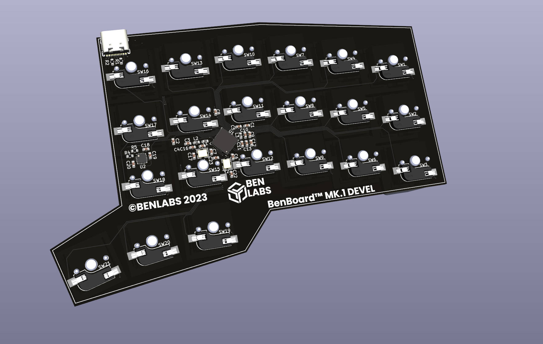
4 layers140 × 88.4 mmBenboard, the printed circuit board in 3D

The BenBoard Split Ergo Mechanical Keyboard

Size
140 × 88.4 mm
Copper layers
4
Thickness
1.61 mm
Parts
111
Nets
94
Pads
974
Tracks, vias
416, 35
Pours
1
Routed
Yes
KiCad
KiCad 8.0 (file 20240108)
Created
26 Jul 2023
Updated
23 Aug 2024

Overview

Benboard is an open-source printed circuit board by ben-labs-ltd, from the ben-labs-ltd/benboard repository on GitHub, published under the GPL-3.0 licence. It is a 4-layer board of 140 × 88.4 mm with 111 parts on 94 nets, routed with 416 tracks and 35 vias.

It is built around the TPS61222DCK and PRTR5V0U2X. Its parts include 27 capacitors, 22 switches, 7 inductors, 5 connectors and 4 resistors. It belongs with the keyboards and input boards and the nRF52 and nRF5x boards of this library.

Main components

2

README

README.md

BenBoard

benboard logo benboard svg

The highly customisable, open source, premium 42 key ergo mechanical keyboard

Show your interest at https://ben-labs.co.uk

Features

  • Reduced layout 42 key split keyboard
  • Cherry MX hotswap compatable (any 3 or 5 pin)
  • Fully wireless (BLE)
  • Month-long battery life with the low power NRF52840
  • Out of the box ZMK Support
  • Supports VIK (on both sides!)
  • Unibody case that has been verified to be CNC'able

Contribution

[ ] TODO

VIK Certification

CategoryClassificationResponse
FPC connectorRequired:heavy_check_mark:
Breakout pinsRecommended:x:
Supplies: SPIRequired:heavy_check_mark:
Supplies: I2CRequired:heavy_check_mark:
I2C on main PCBDiscouraged:x:
I2C pull upsInformative:x:
Supplies: RGBRequired:heavy_check_mark:
Supplies: Extra GPIO 1Required:heavy_check_mark: (Analogue and Digital)
Supplies: Extra GPIO 2Required:heavy_check_mark: (Analogue and Digital)

THIS IS A WORK IN PROGRESS, ANY FEATURES LISTED ARE PURELY IN PROGRESS

Parts

111
QtyValueFootprintReferences
21SW_Pushfingerpunch:gateron-ks27-choc-v1-mx-hotswap-reversibleSW1, SW2, SW3, SW4, SW10, SW11, SW12, SW13, SW14, SW15, SW16, SW17, SW18, SW19, SW20, SW21 +5
18ProbeTestPoint:TestPoint_Pad_D1.0mmTP1, TP2, TP3, TP4, TP5, TP6, TP7, TP10, TP11, TP12, TP13, TP14, TP15, TP16, TP17, TP18 +2
6100nFCapacitor_SMD:C_0805_2012Metric_Pad1.18x1.45mm_HandSolderC6, C10, C11, C12, C24, C26
6LOGOLOGOG***, G***, G***, G***, G***, G***
410uFCapacitor_SMD:C_0805_2012Metric_Pad1.18x1.45mm_HandSolderC18, C19, C20, C25
412pFCapacitor_SMD:C_0805_2012Metric_Pad1.18x1.45mm_HandSolderC16, C17, C22, C23
41uFCapacitor_SMD:C_0805_2012Metric_Pad1.18x1.45mm_HandSolderC1, C3, C13, C15
34.7uFCapacitor_SMD:C_0805_2012Metric_Pad1.18x1.45mm_HandSolderC2, C5, C9
347kInductor_SMD:L_0805_2012Metric_Pad1.15x1.40mm_HandSolderR1, R3, R4
3LEDLED_SMD:LED_0805_2012Metric_Pad1.15x1.40mm_HandSolderD1, D2, D3
210uHInductor_SMD:L_0805_2012Metric_Pad1.15x1.40mm_HandSolderL1, L3
22.2uHInductor_SMD:L_0805_2012Metric_Pad1.15x1.40mm_HandSolderL6, L7
1
10.5pFCapacitor_SMD:C_0805_2012Metric_Pad1.18x1.45mm_HandSolderC14
10.8pFCapacitor_SMD:C_0805_2012Metric_Pad1.18x1.45mm_HandSolderC21
1100pFCapacitor_SMD:C_0805_2012Metric_Pad1.18x1.45mm_HandSolderC7
115nHInductor_SMD:L_0805_2012Metric_Pad1.15x1.40mm_HandSolderL2
12.2uFCapacitor_SMD:C_0805_2012Metric_Pad1.18x1.45mm_HandSolderC27
1250kInductor_SMD:L_0805_2012Metric_Pad1.15x1.40mm_HandSolderR2
132.768kHzCrystal:Crystal_SMD_SeikoEpson_FA238V-4Pin_3.2x2.5mmY2
132MHzCrystal:Crystal_SMD_SeikoEpson_FA238V-4Pin_3.2x2.5mmY1
14.1nHInductor_SMD:L_0805_2012Metric_Pad1.15x1.40mm_HandSolderL4
14.7uHInductor_SMD:L_0805_2012Metric_Pad1.15x1.40mm_HandSolderL5
147nFCapacitor_SMD:C_0805_2012Metric_Pad1.18x1.45mm_HandSolderC4
1820pFCapacitor_SMD:C_0805_2012Metric_Pad1.18x1.45mm_HandSolderC8
1Conn_01x02_PinConnector_JST:JST_EH_B2B-EH-A_1x02_P2.50mm_VerticalJ4
1Conn_ARM_SWD_TagConnect_TC2030-NLConnector:Tag-Connect_TC2030-IDC-NL_2x03_P1.27mm_VerticalJ3
1Conn_CoaxialConnector_Coaxial:U.FL_Hirose_U.FL-R-SMT-1_VerticalJ5
1PRTR5V0U2XPackage_TO_SOT_SMD:SOT-143D4
1SW_DPDTfingerpunch:SW_CuK_OS102011MA1QN1_SPDT_AngledSW22
1TPS61222DCKPackage_TO_SOT_SMD:Texas_R-PDSO-G6U2
1USB_C_Receptacle_USB2.0Connector_USB:USB_C_Receptacle_G-Switch_GT-USB-7010ASVJ1
1nPM1300-QEXXPackage_DFN_QFN:QFN-32-1EP_5x5mm_P0.5mm_EP3.6x3.6mm_ThermalViasU3
1nRF52840Package_DFN_QFN:Nordic_AQFN-73-1EP_7x7mm_P0.5mmU1
1~vik:vik-keyboard-connector-horizontalJ2

The 99 most common of 111 parts.

Similar boards

  • 4 layers24.4 × 35.6 mmAFE 03, the printed circuit board in 3D

    AFE 03

    NeDaMo93/Wearable_ECG_ADS1293_nrf52840

    Software for a Functional Demonstrator of a Medical Wearable for ECG and Activity Monitoring with Wireless Communication. With ADS1293, nrf52840, LSM6DSO. Includes an Android App and Python GUI.

    41 parts7
  • 2 layers44.8 × 36 mmPanel, the printed circuit board in 3D

    Panel

    jeffc/nrf52-watch-obsolete

    obsolete repository - see https://github.com/jeffc/nrf52-watch-firmware

    68 parts6
  • 4 layers25.4 × 20 mm520nm i2c 16mA, the printed circuit board in 3D

    520nm i2c 16mA

    iorodeo/i_control_led

    Hardware files for IO Rodeo's current controlled led for the open colorimeter

    32 parts3CC-BY-4.0
  • 2 layers58.4 × 127 mmExternalPCB, the printed circuit board in 3D

    ExternalPCB

    Kllngii/Wetterstation

    Es sollen mit einem Mikrocontroller mehrere Sensordaten erfasst und aufbereitet werden

    31 parts2
  • 2 layersMeshtastic node, the printed circuit board in 3D

    Meshtastic node

    ben-labs-ltd/BL-N305X

    Meshtastic intended LoRa Node - Ben Labs Node 30.5dBm

    115 parts1MIT
  • 4 layers40.5 × 80.2 mmNULL, the printed circuit board in 3D

    NULL

    jadenvv/NULL

    A version of a flipperzero that has the same capabilities of Sub-GHz RF, IR, Wifi, and NFC/RFID

    121 parts1
  • 2 layers100.1 × 50.8 mmStm32, the printed circuit board in 3D

    Stm32

    jonatlib/stm32-433mhz

    Testing program stm32-433mhz

    59 parts1
  • 4 layers63.8 × 50.8 mmV2 reference, the printed circuit board in 3D

    V2 reference

    ameesme/little-camera

    A small black-and-white camera that posts to its own tiny blog, and everything around it.

    85 partsMIT

Questions

How big is the Benboard PCB?

It measures 140 × 88.4 mm and has 4 copper layers, 1.61 mm thick.

What parts does the Benboard use?

111 parts, built around the TPS61222DCK and PRTR5V0U2X. The full list of its parts is on this page, with links to each part's symbol and footprint where PCBKit's library has them.

Where can I download the Benboard KiCad files?

From the ben-labs-ltd/benboard repository on GitHub, at the commit this page was made from: the board is kicad/benboard-2024-08-23_101722/benboard.kicad_pcb and its schematic kicad/benboard.kicad_sch. PCBKit opens the board in the browser, with nothing to install.

Can I use the Benboard design in my own project?

Its repository publishes it under the GPL-3.0 licence: you may reuse it on that licence's terms (keep the author's notice, and for a copyleft licence share your changes alike).