
2 layers297.2 × 180.3 mm

The KiCad schematic of the board described in docs/hardware.md.
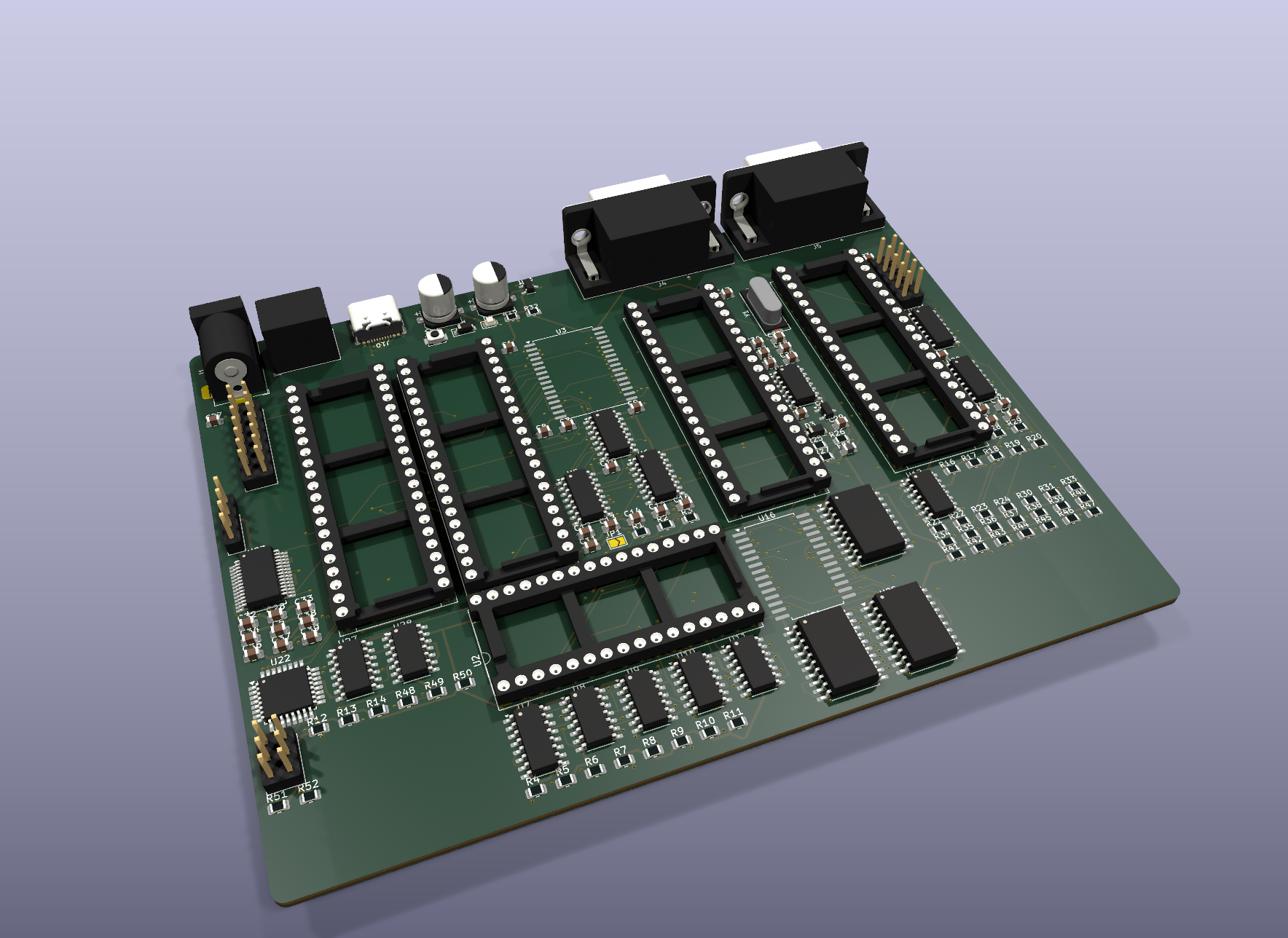
Zl80 is an open-source printed circuit board by bemelab, from the bemelab/Fantasy-retro-Z80-console repository on GitHub. It is a 4-layer board of 138 × 105 mm with 134 parts on 196 nets, routed with 4,168 tracks and 447 vias.
It is built around the 74HCT32D, 74HCT04D and 1N5819HW. Its parts include 52 resistors, 38 capacitors, 26 ICs, 6 connectors and 3 diodes. It belongs with the AVR (ATmega, ATtiny) boards of this library.


The KiCad schematic of the board described in docs/hardware.md.
Not built or tested. Check every pin against the datasheets before you order a board.
Pictures of every schematic page, the copper layers and the 3D views are in hardware/images. They are exported with kicad-cli (sch export svg, pcb export svg, pcb render); export them again after changing the board.
| File | What it is |
|---|---|
zl80.kicad_pro, zl80.kicad_sch | The KiCad project and its root sheet (KiCad 7 format; KiCad 8 and 9 open it). The root sheet has one box per page; double-click a box to open the page. |
cpu_memory.kicad_sch | Page 2: Z80, flash, SRAM, page registers, I/O decoding. |
video.kicad_sch | Page 3: TMS9918A, VRAM (62256 and latches), crystal, video output stage. |
sound.kicad_sch | Page 4: AY-3-8910, its bus control, joystick multiplexers, DB9 ports, audio mix. |
keyboard_usb.kicad_sch | Page 5: 82C55, ATmega328P and the PS/2 header, expansion header, FT245RL USB FIFO and USB-C socket. |
power_tv.kicad_sch | Page 6: 12 V input, 5 V regulator, reset, and the TV header for a SCART cable. |
zl80.kicad_sym, sym-lib-table | The board's symbols as a project library, so KiCad finds the zl80 library. |
gen_schematic.py | Generates the schematic. Change the circuit here, not in KiCad. |
sch.py | The small schematic writer that gen_schematic.py uses. |
check_schematic.py | Checks that the file parses and that every pin is either connected or marked as not connected. |
zl80-netlist.txt | Every net with the pins on it, for checking against datasheets. |
check_footprints.py | Checks that every part's footprint exists in KiCad's library and has a pad for each symbol pin. |
zl80.kicad_pcb | The routed 4-layer board, 138 x 105 mm: tracks on F.Cu, In2.Cu and B.Cu, a whole GND plane on In1.Cu, a +5V fill on In2.Cu. |
zl80.dsn, zl80.ses | What went to Freerouting and the routes it sent back. gen_pcb.py import zl80.ses restores the tracks after gen_pcb.py has placed the parts again. |
gen_pcb.py | Builds the board with KiCad's Python: places the parts, draws the outline and planes, writes zl80.dsn for Freerouting, and reads the routed .ses back. |
To regenerate the schematic and run the check:
python gen_schematic.py
python check_schematic.py
With KiCad installed, also run its electrical rules check; it should report 0 violations. The netlist KiCad exports has the same 187 nets as zl80-netlist.txt (KiCad leaves out the PWR_FLAG markers).
kicad-cli sch erc --severity-all zl80.kicad_schgen_pcb.py runs with KiCad's own Python (KiCad's bin folder must be on PATH). It reads the parts and nets from gen_schematic.py, so the board always matches the schematic.
set PATH=D:\Program Files\KiCad\9.0\bin;%PATH%
python gen_pcb.py                      (KiCad's python.exe) places the parts, writes zl80.kicad_pcb and zl80.dsn
freerouting-cli -de zl80.dsn -do zl80.ses -mp 100
python gen_pcb.py import zl80.ses      adds the routed tracks to zl80.kicad_pcb
kicad-cli pcb drc zl80.kicad_pcb
Freerouting 2.5.0 routed the board in about 25 minutes (-mp 200). Two settings in the DSN that gen_pcb.py writes make that work: only the GND net may use In1.Cu, so the GND plane stays whole and GND pads reach it through vias, and the routing boundary sits 0.55 mm inside the board edge. KiCad's DRC with the schematic parity check reports 0 violations, 0 unconnected pads and 0 footprint errors; what is left are silkscreen warnings (labels over pads and over each other), which the board maker clips.
Placement: the 12 V jack, the regulator, the USB-C socket and both joystick ports along the top edge; below them one row of the four DIP-40 sockets (82C55, Z80, TMS9918A, AY-3-8910 from left to right); each group's surface-mount parts are packed beside and below its socket, each chip next to its own 100 nF capacitor. All surface-mount parts are on the top side, so the board needs assembly on one side only. Design rules: 0.15 mm clearance, 0.2 mm tracks, 0.6/0.3 mm vias, all inside JLCPCB's 4-layer limits.
100n (U15).~{RD}.| Qty | Value | Footprint | References |
|---|---|---|---|
| 30 | 10k | R_0805_2012Metric | R1, R2, R3, R4, R10, R11, R12, R15, R33, R34, R35, R36, R37, R38, R39, R40 +14 |
| 6 | 1k | R_0805_2012Metric | R19, R22, R29, R30, R31, R32 |
| 3 | 100n | C_0805_2012Metric | C5, C29, C36 |
| 3 | 3k | R_0805_2012Metric | R16, R17, R18 |
| 3 | 4.7k | R_0805_2012Metric | R13, R14, R48 |
| 2 | 100n (U23) | C_0805_2012Metric | C32, C38 |
| 2 | 100u | CP_Elec_6.3x7.7 | C3, C4 |
| 2 | 10u | C_0805_2012Metric | C1, C2 |
| 2 | 1N5819HW | D_SOD-123 | D1, D3 |
| 2 | 2.2k | R_0805_2012Metric | R20, R21 |
| 2 | 22p | C_0805_2012Metric | C30, C31 |
| 2 | 47k | R_0805_2012Metric | R23, R24 |
| 2 | 5.1k | R_0805_2012Metric | R51, R52 |
| 2 | 74HCT32 | SOIC-14_3.9x8.7mm_P1.27mm | U8, U9 |
| 2 | 75 | R_0805_2012Metric | R27, R28 |
| 1 | 10.738635 MHz | Crystal_SMD_HC49-SD | Y1 |
| 1 | 100n (U1) | C_0805_2012Metric | C6 |
| 1 | 100n (U10) | C_0805_2012Metric | C16 |
| 1 | 100n (U11) | C_0805_2012Metric | C11 |
| 1 | 100n (U12) | C_0805_2012Metric | C24 |
| 1 | 100n (U15) | C_0805_2012Metric | C17 |
| 1 | 100n (U16) | C_0805_2012Metric | C22 |
| 1 | 100n (U17) | C_0805_2012Metric | C18 |
| 1 | 100n (U18) | C_0805_2012Metric | C23 |
| 1 | 100n (U19) | C_0805_2012Metric | C25 |
| 1 | 100n (U2) | C_0805_2012Metric | C7 |
| 1 | 100n (U20) | C_0805_2012Metric | C26 |
| 1 | 100n (U21) | C_0805_2012Metric | C27 |
| 1 | 100n (U22) | C_0805_2012Metric | C28 |
| 1 | 100n (U24) | C_0805_2012Metric | C19 |
| 1 | 100n (U25) | C_0805_2012Metric | C20 |
| 1 | 100n (U26) | C_0805_2012Metric | C21 |
| 1 | 100n (U27) | C_0805_2012Metric | C33 |
| 1 | 100n (U28) | C_0805_2012Metric | C34 |
| 1 | 100n (U3) | C_0805_2012Metric | C8 |
| 1 | 100n (U4) | C_0805_2012Metric | C9 |
| 1 | 100n (U5) | C_0805_2012Metric | C10 |
| 1 | 100n (U6) | C_0805_2012Metric | C12 |
| 1 | 100n (U7) | C_0805_2012Metric | C13 |
| 1 | 100n (U8) | C_0805_2012Metric | C14 |
| 1 | 100n (U9) | C_0805_2012Metric | C15 |
| 1 | 10n | C_0805_2012Metric | C39 |
| 1 | 12 V DC in | BarrelJack_Horizontal | J1 |
| 1 | 130 | R_0805_2012Metric | R25 |
| 1 | 4.7u | C_0805_2012Metric | C37 |
| 1 | 470 | R_0805_2012Metric | R26 |
| 1 | 62256 VRAM (16 KB used) | SOP-28_8.4x18.16mm_P1.27mm | U16 |
| 1 | 74HCT02 AY bus control, USB WR | SOIC-14_3.9x8.7mm_P1.27mm | U12 |
| 1 | 74HCT04 | SOIC-14_3.9x8.7mm_P1.27mm | U10 |
| 1 | 74HCT04 VRAM strobes | SOIC-14_3.9x8.7mm_P1.27mm | U26 |
| 1 | 74HCT125 USB status on D0, D1 | SOIC-14_3.9x8.7mm_P1.27mm | U28 |
| 1 | 74HCT138 I/O 00h-7Fh | SOIC-16_3.9x9.9mm_P1.27mm | U7 |
| 1 | 74HCT138 I/O 80h-BFh | SOIC-16_3.9x9.9mm_P1.27mm | U6 |
| 1 | 74HCT157 joystick buttons | SOIC-16_3.9x9.9mm_P1.27mm | U20 |
| 1 | 74HCT157 joystick directions | SOIC-16_3.9x9.9mm_P1.27mm | U19 |
| 1 | 74HCT32 USB FIFO strobes | SOIC-14_3.9x8.7mm_P1.27mm | U27 |
| 1 | 74HCT574 VRAM column latch | SOIC-20W_7.5x12.8mm_P1.27mm | U24 |
| 1 | 74HCT574 VRAM row latch | SOIC-20W_7.5x12.8mm_P1.27mm | U17 |
| 1 | 74HCT574 VRAM write data | SOIC-20W_7.5x12.8mm_P1.27mm | U25 |
| 1 | 74HCT670 page bits 0-3 | SOIC-16_3.9x9.9mm_P1.27mm | U4 |
| 1 | 74HCT670 page bits 4-5 | SOIC-16_3.9x9.9mm_P1.27mm | U5 |
| 1 | 74HCT74 paging on / AY clock | SOIC-14_3.9x8.7mm_P1.27mm | U11 |
| 1 | 82C55A | DIP-40_W15.24mm_Socket | U21 |
| 1 | AS6C4008 SRAM, pages 32-63 | SOP-32_11.305x20.495mm_P1.27mm | U3 |
| 1 | ATmega328P-AU: PS/2 to key matrix | TQFP-32_7x7mm_P0.8mm | U22 |
| 1 | AY-3-8910 | DIP-40_W15.24mm_Socket | U18 |
| 1 | DS1813-5 reset | SOT-23-3 | U13 |
| 1 | Expansion (8255 PA, PC4-7) | PinHeader_2x07_P2.54mm_Vertical | J8 |
| 1 | FT245RL USB FIFO | SSOP-28_5.3x10.2mm_P0.65mm | U23 |
| 1 | Ferrite bead | L_0805_2012Metric | FB1 |
| 1 | Flash write enable | SolderJumper-2_P1.3mm_Open_TrianglePad1.0x1.5mm | JP1 |
| 1 | ISP for the ATmega | PinHeader_2x03_P2.54mm_Vertical | J7 |
| 1 | Joystick 1 (Atari / Sega) | DSUB-9_Male_Horizontal_P2.77x2.84mm_EdgePinOffset7.70mm_Housed_MountingHolesOffset9.12mm | J4 |
| 1 | Joystick 2 (Atari / Sega) | DSUB-9_Male_Horizontal_P2.77x2.84mm_EdgePinOffset7.70mm_Housed_MountingHolesOffset9.12mm | J5 |
| 1 | MMBT4401 video buffer | SOT-23-3 | Q1 |
| 1 | PS/2 keyboard (panel socket) | PinHeader_1x04_P2.54mm_Vertical | J6 |
| 1 | Power | LED_0805_2012Metric | D2 |
| 1 | R-78E5.0-1.0 (or 7805) | Converter_DCDC_RECOM_R-78E-0.5_THT | U14 |
| 1 | Reset | SW_SPST_B3U-1000P | SW1 |
| 1 | SST39SF040 flash, pages 0-31 | DIP-32_W15.24mm_Socket | U2 |
The 130 most common of 134 parts.

tebl/RC6502-Apple-1-Replica
An expandable SBC-version of the Apple 1 computer, easy to get started with and lot of cool stuff that can be added to it!


leomil72/LM80C
A Z80-based homebrew computer withTMS9918, AY-3-8910, Z80 CTC, Z80 PIO, and Z80 SIO

MarkJelic/TEC-1G
The new incarnation of the 40 year old Z80 trainer computer - Now with Fulisik LEDs!


b3rendsh/msxdos2s
MSXDOS smaller 16K/32K rom with IDE interface drivers and enhancements

It measures 138 × 105 mm and has 4 copper layers, 1.6 mm thick.
134 parts, built around the 74HCT32D, 74HCT04D and 1N5819HW. The full list of its parts is on this page, with links to each part's symbol and footprint where PCBKit's library has them.
From the bemelab/Fantasy-retro-Z80-console repository on GitHub, at the commit this page was made from: the board is hardware/kicad/zl80.kicad_pcb and its schematic hardware/kicad/cpu_memory.kicad_sch. PCBKit opens the board in the browser, with nothing to install.
Its repository states no licence, so its author keeps all rights: ask bemelab before reusing the design.