10 layers366.8 × 206 mm
Redux
bcrist/16717a
I would not recommend attempting to build one of these boards unless you have and know how to use the following equiment:
1,081 parts

 bcrist/16717a
I would not recommend attempting to build one of these boards unless you have and know how to use the following equiment:
Original is an open-source printed circuit board by bcrist, from the bcrist/16717a repository on GitHub. It is an 8-layer board of 365.8 × 205 mm with 2,101 parts on 1,868 nets, routed with 31,706 tracks and 4,783 vias.
It is built around the MC100LVEL16D, AD7841AS and MC100LVEL11D, with the 74LVC08AD, LM2991T and LM311 among its other parts. Its parts include 411 capacitors, 279 resistors, 72 ICs, 68 fuses and 15 connectors.


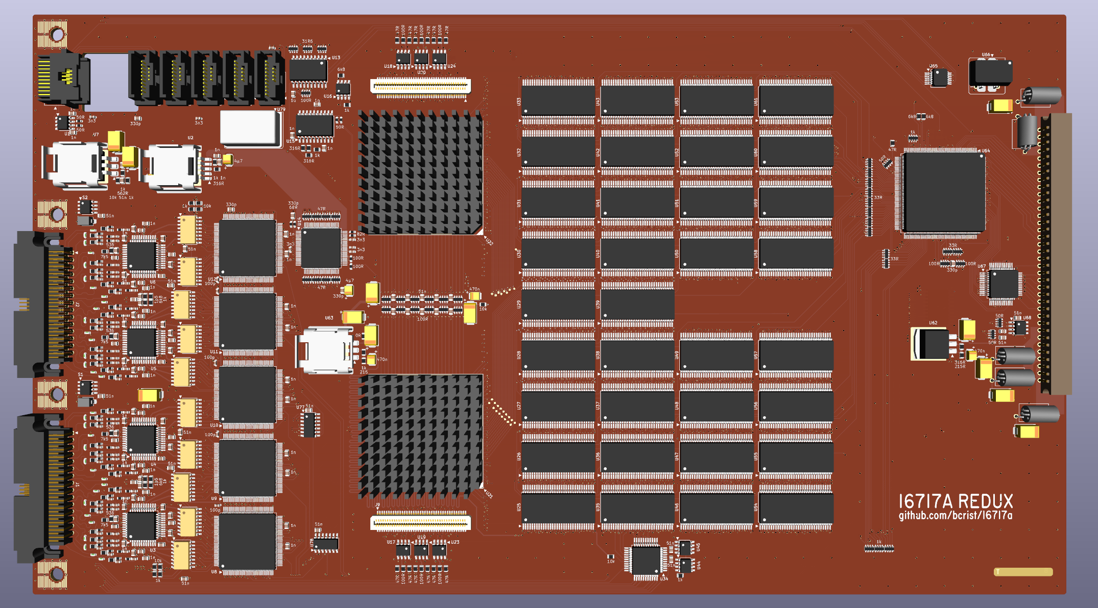
I would not recommend attempting to build one of these boards unless you have and know how to use the following equiment:
While reverse engineering the 16717A I noticed a lot of potential signal integrity issues:
I'm sure that HP did a ton of testing to ensure there were no real world performance or EMI issues because of this, but since I don't know exactly what FR4 stackup they used, nor the dielectric constant of their core/prepreg layers, I decided it would be better to rework some things and go to a 10-layer design instead. For small quantities of large size boards, 10-layer boards through JLCPCB are only a little more expensive than 8 layers (relatively speaking), and their default stackup for 10 layers is a bit nicer as well.
Here is the layer ordering I chose:
The most important goal here is to ensure that all signal layers are adjacent to ground plane layers. No two signal layers are adjacent to each other, and all stripline layers have ground on both sides, not just one. Additionally, since the board is quite large, the ground and power layers are symetrical to avoid any twist/bend from copper imbalance. The inner power layers (layer 5 and 6), rather than having having one +5V and one +3.3V layer, are routed with mostly identical planes covering only areas that need 5V and +3.3V separately, to avoid coupling noise from one rail to the other.
Trace widths were selected assuming JLCPCB's default 10 layer stackup (JLC10161H-2116) with 1oz outer copper and 0.5oz inner copper. If you choose to have it manufactured elsewhere, you might need to adjust them. For reference, JLC10161H-2116 uses four 0.2mm cores (Er = 4.6) and five 4.7mil prepregs (Er = 4.16).
All 0.3mm holes should be epoxy filled and capped (JLCPCB should do this by default for 6+ layer boards).
JLCPCB will charge an extra $15 for any design with more than 4000 holes under 0.5mm in diameter. This is listed on their "special cases" page, but it isn't described very clearly, and at the time of writing isn't included in their automated quoting tool. To avoid hitting this limit, most power vias in the design have been set to 0.5mm. All of the 0.5mm holes on the board may be filled and capped, but it shouldn't be a problem if they are not.
Note that even working to avoid the extra drilling charges, JLCPCB will likely charge an additional $7.50 above their quoted price for this board. After inquiring they informed me this was due to the large number of electrical test points, though they didn't tell me exactly what the limit is before that kicks in; I decided it wasn't worth pursuing that since there's not much I could do to reduce the number of pads in the design anyway.
It is by no means necessary to follow these exact procedures, however if you are concerned about parts having been potentially damaged in removal from the old board, this guide allows incrementally verifying some subsystems with a minimum of time sunk into soldering hundreds of passive components.
Note: I highly recommend checking all power rails for shorts after each step below, before powering up the mainframe. The 167xx power supplies do not seem to have short-circuit protection. I once accidentally plugged in an original 16717A "upside-down" and ended up blowing the PSU (and maybe the FPGA on the 16717A too; it wasn't working beforehand so I can't be sure). I was using a ribbon cable backplane extender, and forgot that the mainframe was sitting on my desk upside down. doh! After replacing the PSU the mainframe still works fine, thankfully. I was afraid I might have blown the backplane interface board as well, but it seems to still work fine.
For the vast majority of the passive components, you can just use new parts of the same value. Indeed, since I replaced a bunch of resistors and SOIC resistor networks with more modern 0612 (4x0603) resistor networks, you'll need to use new parts for those. But almost all the semiconductors and connectors used are either custom, obsolete, or expensive, so you'll need to salvage parts from a donor board (presumably non-working only because of trace/via corrosion). In particular, you'll need:
The first goal is to get a 16700A/B to recognize the board as a 16717A module, which indicates that the FPGA isn't completely dead, and is able to communicate with the backplane. The main parts that need to be populated for this test are:
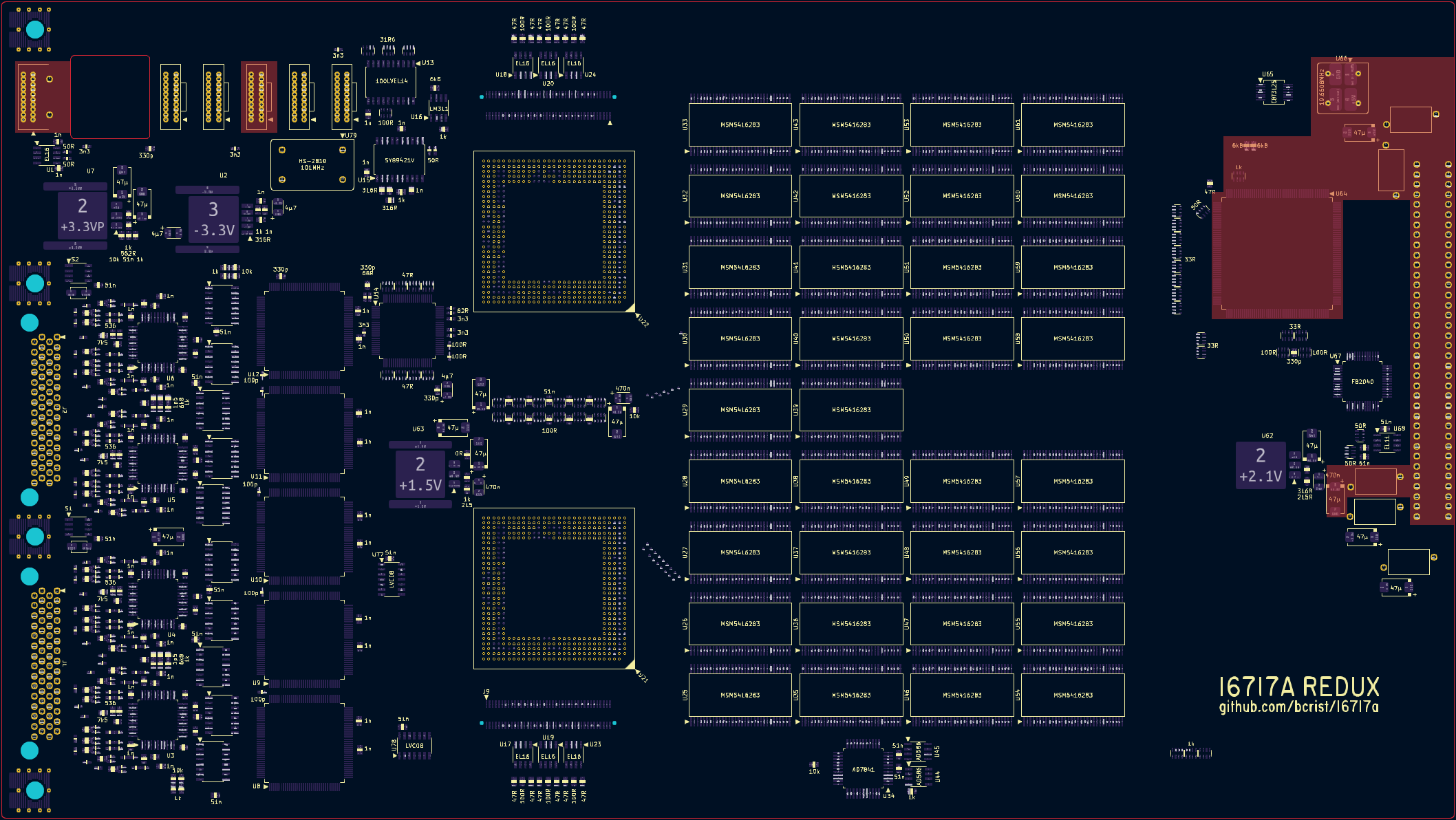
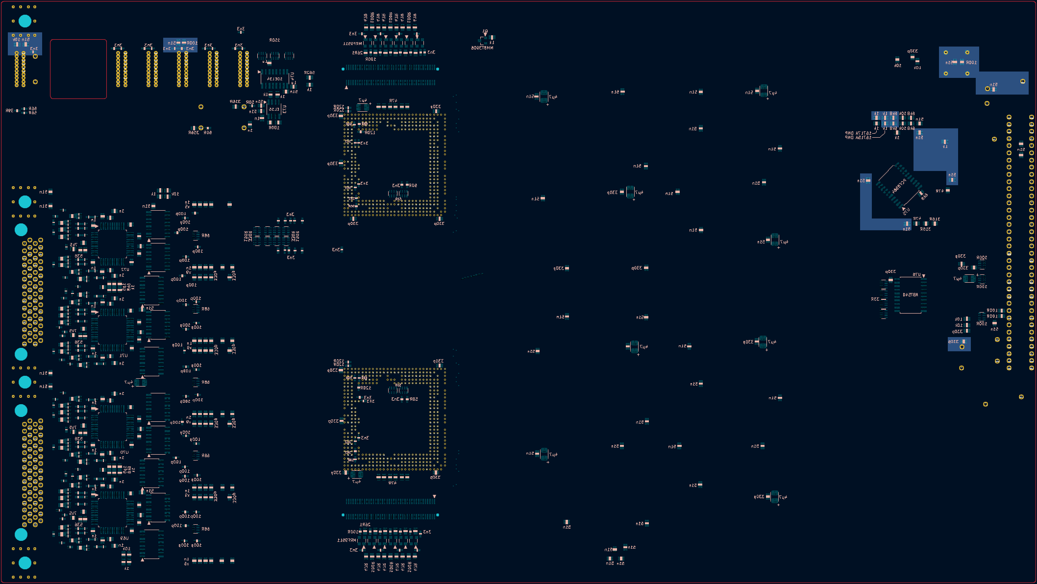
Note: I don't recommend installing the back panel bracket/screws yet. You can use zip ties to create pull loops for removing the board from a mainframe after testing.
Once these components have been populated, the board should be selectable in pv, but all of the tests should fail:
$ pv
Shared Memory Segment 204 attached at Virtual Address: 0xc0dbf000
DMA Shared Memory is mapped to Physical Address: 0x4e9b000
Second half of DMA Shared Memory is mapped to Physical Address: 0x4c57000
RPC system Initialized (Program=700016505, Version=1)
pv> l
# Model 16702B
# System Memory=256 Mbytes, PCI device=1, PCI driver=1.01
Mod CPU: System CPU Board
Mod PCI: 16702B System PCI Board
Mod A  : Empty slot
Mod B  : (0x2e) 16717A 333MHz State/2GHz Timing Zoom 2M Sample
Mod C  : Empty slot
Mod D  : Empty slot
Mod E  : Empty slot
Mod 1  : Empty slot
Mod 2  : Empty slot
pv> s b
Module index=B
pv> x modtests
Mod   B: TEST FAILED       # "vramDataTest" (1, 1, -1)
Mod   B: TEST FAILED       # "vramAddrTest" (1, 1, -1)
Mod   B: TEST FAILED       # "vramCellTest" (1, 1, -1)
Mod B: TEST FAILED # "vramUnloadTest" (1, 1, -1)You may see bpClkTest report a pass, but it's a false-positive. If you run the test with debug mode enabled, you can see that the test is only checking for a frequency above certain thresholds.
The PLLs mentioned are inside the acquisition ASICs, so without them populated, it's just picking up random interference. If it happens to get a "frequency" over 158 MHz, it will consider the test successful.
pv> x bpClkTest
  Mod B: Measurement Did Not Complete.
  Testing 100 MHz - PLL bypass mode:
    Slot B, Chip 9: exp: > 9500000, actual: 151783694
    Slot B, Chip 8: exp: > 9500000, actual: 151783694
  Testing PLL at 166.67 MHz:
    Slot B, Chip 9: exp: >15833333, actual: 151783694
    Slot B, Chip 8: exp: >15833333, actual: 151783694
You may or may not see the "Unable to Detect WRAP Flag" lines, but if they do appear, they should go away once the remaining passives around the FPGA are populated.
By far the most difficult parts to solder are the two ASIC BGAs, so as soon as possible, we want to get them populated and verify that they haven't been destroyed by reflowing. You may even want to do these before populating the FPGA components in the previous section.
If you're not comfortable reballing and soldering BGAs I'd suggest practicing on something less rare/useful first. You may find the bga_stencil directory useful when reballing the chips. Once reballed, I found that soldering the chips with a hotplate only worked best. Use polyimide tape to protect the soldermask while clamping the board to a hotplate (clamping is necessary to prevent any warping) and avoid using any hot air from above. Too much heat can cause the interposer to warp slightly. If this happens too much it may cause some of the outer balls to not make contact. Heating only through the board itself helps prevent this. Wait for the board to fully cool before unclamping it from the hotplate.
After soldering, use a multimeter in diode/resistance/continuity mode to check that each of the test points on the back side of the board has a solid connection to the chip. There are also a few test points on the top side for signals that never traverse a via.
Once you are confident that all the BGA balls are attached properly, you can install the remaining components for the next test:
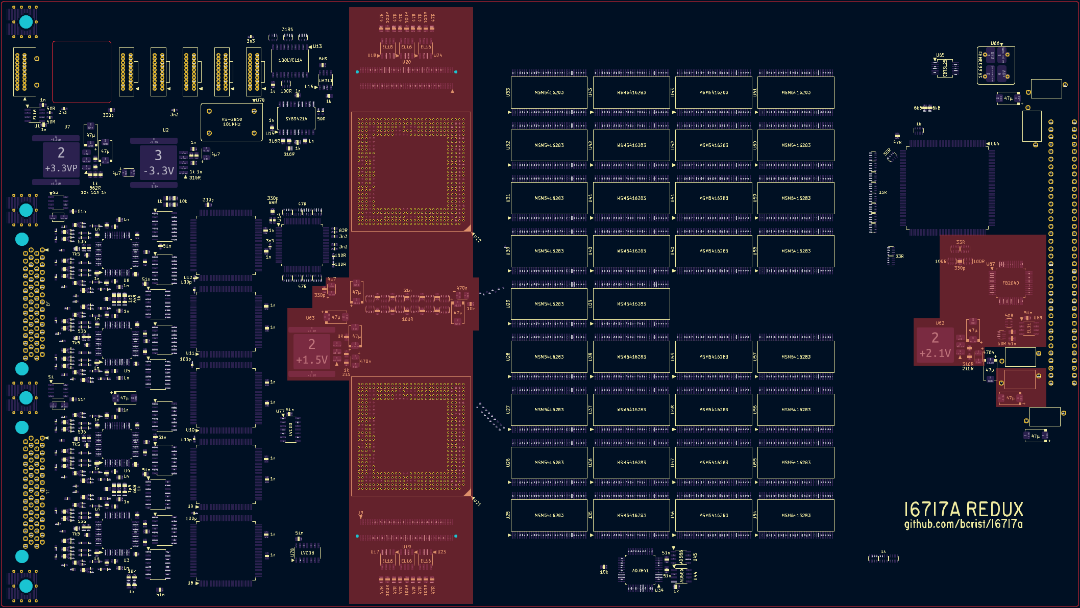
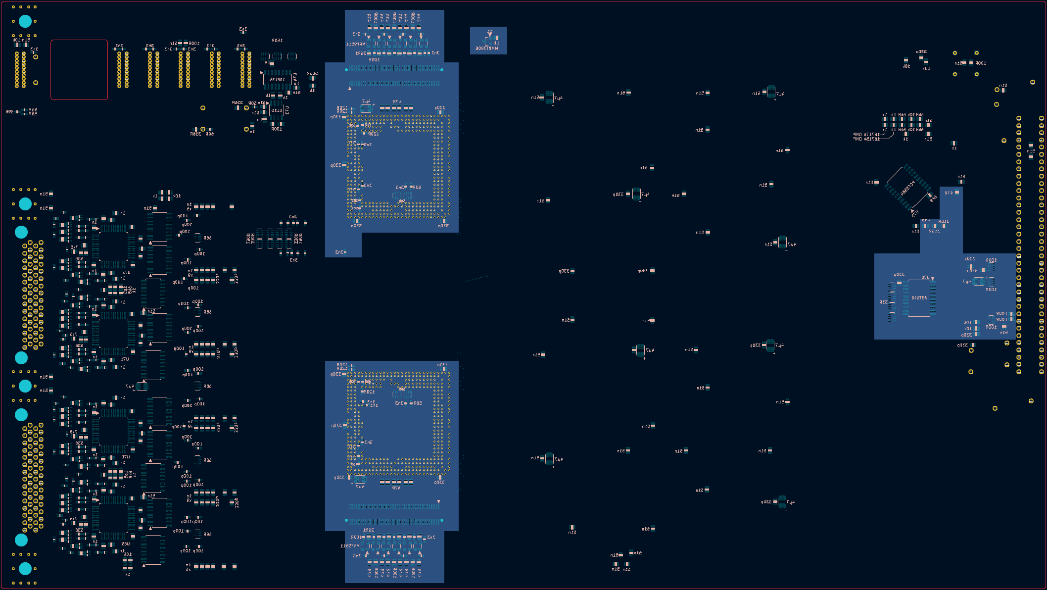
It's probably not necessary for testing at this point, but I would recommend reattaching the ASIC heatsinks with some thermal compound before any attempt to power up the board. I forgot this during one test, yet after running pv tests and then idling for a few minutes and shutting down the system, the heatspreaders felt cold to the touch. Yet HP put large heatsinks on these chips for a reason. Perhaps they only put out significant heat when running a high speed acquisition, but better to be safe than sorry.
With these components now populated, pv should show the board passing chipRegTest, bpClkTest, icrTest, flagTest, and armTest:
pv> x modtests
Mod   B: TEST FAILED       # "vramDataTest" (1, 1, -1)
Mod   B: TEST FAILED       # "vramAddrTest" (1, 1, -1)
Mod   B: TEST FAILED       # "vramCellTest" (1, 1, -1)
Mod   B: TEST FAILED       # "vramUnloadTest" (1, 1, -1)
Mod   B: TEST passed       # "chipRegTest" (1, 0, 1)
Mod   B: TEST passed       # "bpClkTest" (1, 0, 1)
Mod   B: TEST FAILED       # "cmpTest" (1, 1, -1)
Mod   B: TEST passed       # "icrTest" (1, 0, 1)
Mod   B: TEST passed       # "flagTest" (1, 0, 1)
Mod   B: TEST passed       # "armTest" (1, 0, 1)
Mod   B: TEST FAILED       # "vramSerDataTest" (1, 1, -1)
Mod   B: TEST FAILED       # "vramSerCellTest" (1, 1, -1)
Mod   B: TEST FAILED       # "clksTest" (1, 1, -1)
Mod   B: TEST FAILED       # "calTest" (1, 1, -1)
Mod   B: TEST FAILED       # "zoomDataTest" (1, 1, -1)
Mod   B: TEST FAILED       # "zoomMasterTest" (1, 1, -1)
Mod   B: TEST FAILED       # "fisoRedundancyTest" (1, 1, -1)
  Mod B: Unable to Detect WRAP Flag.  Possible Board Fault.
Mod   B: TEST FAILED       # "zoomAcqTest" (1, 1, -1)
  Mod B: Unable to Detect WRAP Flag.  Possible Board Fault.
  Mod B: Unable to Detect WRAP Flag.  Possible Board Fault.
  Mod B: Unable to Detect WRAP Flag.  Possible Board Fault.
  Mod B: Unable to Detect WRAP Flag.  Possible Board Fault.
Mod   B: TEST FAILED       # "zoomChipSelTest" (1, 1, -1)
If any of the tests shown passing above fail, try setting d d=9 and/or d r=9 and rerunning the failing test to get more details. When pv refers to "Chip 8" it means the one closer to the ribbon cable connectors and 101MHz oscillator. "Chip 9" refers to the ASIC closer to the AD7841 DAC.
If you see bpClkTest reporting a frequency of 0 for both Chip 8 and Chip 9, the problem may lie with the ECL clock buffer near the backplane connector, or one of the passives near it. Check for shorts and verify that it has continueity to the proper ASIC pins. If only one of the chips reports a bad frequencies, but you're reasonably certain that the clock balls are making a good connection, the ASIC may have gone bad.
If flagTest fails, first check the 74FB2040 transceiver or replace it if you have a spare. If that doesn't fix the problem it's probably a bad FPGA or ASIC.
If any of the other tests fail, it's likely due to an unconnected BGA ball somewhere, or a bad ASIC.
Next, populate the 34 DRAM chips, decoupling capacitors beneath them on the bottom side, and the RAS/CAS termination networks on the top side.
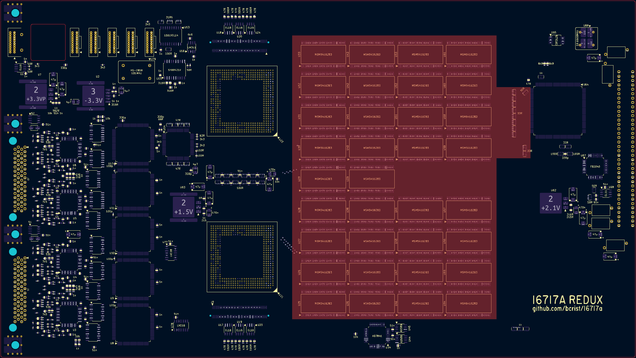
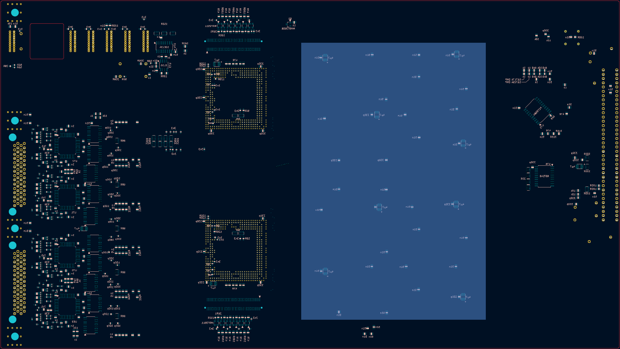
Once these have been populated, pv should report all the vram* tests passing, as well as clksTest, and all of the previously passing tests:
pv> x modtests
Mod   C: TEST passed       # "vramDataTest" (1, 0, 1)
Mod   C: TEST passed       # "vramAddrTest" (1, 0, 1)
Mod   C: TEST passed       # "vramCellTest" (1, 0, 1)
Mod   C: TEST passed       # "vramUnloadTest" (1, 0, 1)
Mod   C: TEST passed       # "chipRegTest" (1, 0, 1)
Mod   C: TEST passed       # "bpClkTest" (1, 0, 1)
Mod   C: TEST FAILED       # "cmpTest" (1, 1, -1)
Mod   C: TEST passed       # "icrTest" (1, 0, 1)
Mod   C: TEST passed       # "flagTest" (1, 0, 1)
Mod   C: TEST passed       # "armTest" (1, 0, 1)
Mod   C: TEST passed       # "vramSerDataTest" (1, 0, 1)
Mod   C: TEST passed       # "vramSerCellTest" (1, 0, 1)
Mod   C: TEST passed       # "clksTest" (1, 0, 1)
Mod   C: TEST FAILED       # "calTest" (1, 1, -1)
Mod   C: TEST FAILED       # "zoomDataTest" (1, 1, -1)
Mod   C: TEST FAILED       # "zoomMasterTest" (1, 1, -1)
Mod   C: TEST FAILED       # "fisoRedundancyTest" (1, 1, -1)
Mod   C: TEST FAILED       # "zoomAcqTest" (1, 1, -1)
Mod   C: TEST FAILED       # "zoomChipSelTest" (1, 1, -1)
If pv reports errors for all chips on vramDataTest or vramAddrTest, it likely means that one or more of the memory data or address lines are shorted together, or shorted to one of the power rails. The easiest way to track this down is with a DMM capable of precisely measuring low-ohm resistances (e.g. HP 3478A). The location of a short will show very near 0 ohms, increasing by around 200 mOhm for the same pins on adjacent DRAMs, and up to several ohms for chips very far from the short. Once you find the short, if there is no solder bridge, the chip is likely damaged internally.
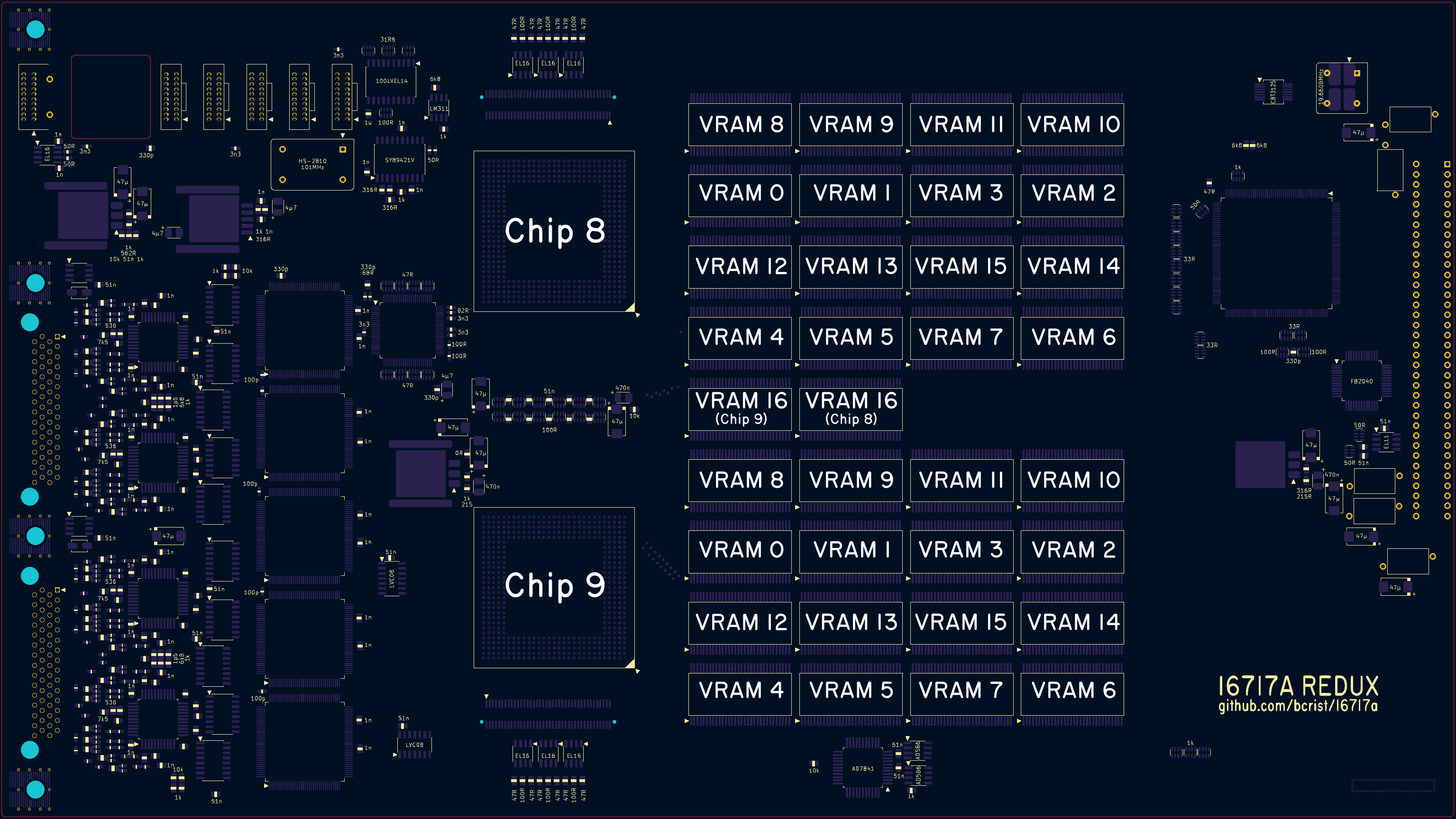
If pv reports errors with only a specific chip, then the problem is likely an unconnected pin, cold solder joint, or internally broken bond wire. this diagram may help track down which one is faulty:
To make progress on the rest of the pv tests, we need to get the internal test clock working. To do this we need to populate:
Some other parts are not actually required by any pv tests, but which are best populated now:
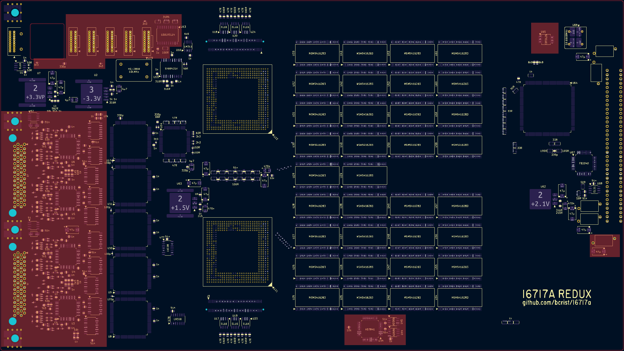
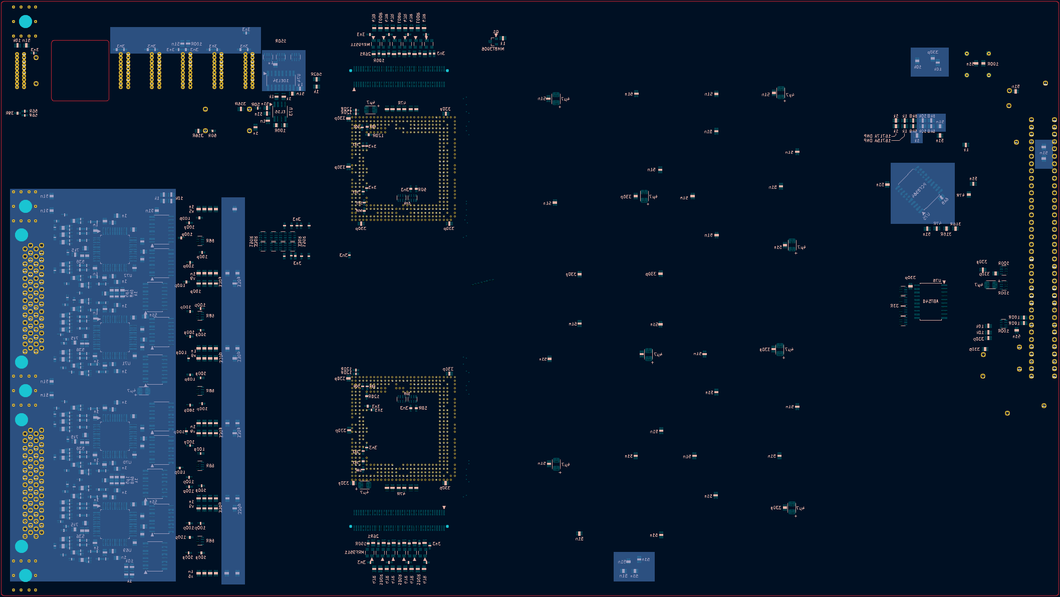
cmpTest and calTest should now pass in pv:
pv> x modtests
Mod   C: TEST passed       # "vramDataTest" (1, 0, 1)
Mod   C: TEST passed       # "vramAddrTest" (1, 0, 1)
Mod   C: TEST passed       # "vramCellTest" (1, 0, 1)
Mod   C: TEST passed       # "vramUnloadTest" (1, 0, 1)
Mod   C: TEST passed       # "chipRegTest" (1, 0, 1)
Mod   C: TEST passed       # "bpClkTest" (1, 0, 1)
Mod   C: TEST passed       # "cmpTest" (1, 0, 1)
Mod   C: TEST passed       # "icrTest" (1, 0, 1)
Mod   C: TEST passed       # "flagTest" (1, 0, 1)
Mod   C: TEST passed       # "armTest" (1, 0, 1)
Mod   C: TEST passed       # "vramSerDataTest" (1, 0, 1)
Mod   C: TEST passed       # "vramSerCellTest" (1, 0, 1)
Mod   C: TEST passed       # "clksTest" (1, 0, 1)
Mod   C: TEST passed       # "calTest" (1, 0, 1)
Mod   C: TEST FAILED       # "zoomDataTest" (1, 1, -1)
Mod   C: TEST FAILED       # "zoomMasterTest" (1, 1, -1)
Mod   C: TEST FAILED       # "fisoRedundancyTest" (1, 1, -1)
Mod   C: TEST FAILED       # "zoomAcqTest" (1, 1, -1)
Mod   C: TEST FAILED       # "zoomChipSelTest" (1, 1, -1)
At this point, the only parts not populated should be zoom-related, and we effectively have a 16715A board that thinks it's a 16717A. In fact, if you move the identification resistor to the 16715A setting, you'll now see all the pv tests pass.
cmpTest DebuggingIf you decide to test with only some of the comparators populated, make sure that you do populate all four of the termination networks for the 50MHz test clock. Otherwise reflections may cause issues even on the comparators that you have populated.
Note: The output of cmpTest with debug result logging enabled can be really useful, but it can also be tricky to decipher. At first glance, it seems like there's way too much output. It can be helpful to see what it looks like when none of the comparators are populated:
pv> d r=9
debugLevel=0, mode=0, resultLevel=9
pv> x cmpTest
  Mod C: Measurement Did Not Complete.
  Check POD1 Thresholds:
    Slot C, Chip 9: . ........ ........  . ........ ........  Cal Clk No Act.
    Slot C, Chip 8: . ........ ........  . ........ ........  Cal Clk No Act.
    Slot C, Chip 9: . ........ ........  B BBBBBBBB BBBBBBBB  Cal Clk Levels
    Slot C, Chip 8: . ........ ........  . ........ ........  Cal Clk Levels
    Slot C, Chip 9: . ........ ........  B BBBBBBBB BBBBBBBB  Cal Clk Activity
    Slot C, Chip 8: . ........ ........  . ........ ........  Cal Clk Activity
  Check POD2 Thresholds:
    Slot C, Chip 9: . ........ ........  . ........ ........  Cal Clk No Act.
    Slot C, Chip 8: . ........ ........  . ........ ........  Cal Clk No Act.
    Slot C, Chip 9: B BBBBBBBB BBBBBBBB  . ........ ........  Cal Clk Levels
    Slot C, Chip 8: . ........ ........  . ........ ........  Cal Clk Levels
    Slot C, Chip 9: B BBBBBBBB BBBBBBBB  . ........ ........  Cal Clk Activity
    Slot C, Chip 8: . ........ ........  . ........ ........  Cal Clk Activity
  Check POD3 Thresholds:
    Slot C, Chip 9: . ........ ........  . ........ ........  Cal Clk No Act.
    Slot C, Chip 8: . ........ ........  . ........ ........  Cal Clk No Act.
    Slot C, Chip 9: . ........ ........  . ........ ........  Cal Clk Levels
    Slot C, Chip 8: . ........ ........  B BBBBBBBB BBBBBBBB  Cal Clk Levels
Slot C, Chip 9: . ........ ........ . ........ ........ Cal Clk ActivityWe can see that it tests each pod individually, and each each test consists of several parts: first testing that all the signals for the pod report high/low when the threshold voltage is well above or below the test clock signal ("Cal Clk No Act." and "Cal Clk Levels") and only then testing that the 50MHz test clock signal is seen on all signals of the pod when the threshold voltage is set in the middle of the test clock ("Cal Clk Activity"). In all three cases, all the comparators for other pods have their thresholds configured so that no signals are seen, so if you see B for any of the . spots above, you probably have a bad comparator or DAC, or maybe a shorted resistor, rather than an open circuit on one of your signal lines.
If there's a problem with the test clock generation, but the DAC is working, you'll see something like this:
pv> x cmpTest
  Mod B: Measurement Did Not Complete.
  Check POD1 Thresholds:
    Slot B, Chip 9: . ........ ........  . ........ ........  Cal Clk No Act.
    Slot B, Chip 8: . ........ ........  . ........ ........  Cal Clk No Act.
    Slot B, Chip 9: . ........ ........  . ........ ........  Cal Clk Levels
    Slot B, Chip 8: . ........ ........  . ........ ........  Cal Clk Levels
    Slot B, Chip 9: . ........ ........  B BBBBBBBB BBBBBBBB  Cal Clk Activity
    Slot B, Chip 8: . ........ ........  . ........ ........  Cal Clk Activity
  Check POD2 Thresholds:
    Slot B, Chip 9: . ........ ........  . ........ ........  Cal Clk No Act.
    Slot B, Chip 8: . ........ ........  . ........ ........  Cal Clk No Act.
    Slot B, Chip 9: . ........ ........  . ........ ........  Cal Clk Levels
    Slot B, Chip 8: . ........ ........  . ........ ........  Cal Clk Levels
    Slot B, Chip 9: B BBBBBBBB BBBBBBBB  . ........ ........  Cal Clk Activity
    Slot B, Chip 8: . ........ ........  . ........ ........  Cal Clk Activity
  Check POD3 Thresholds:
    Slot B, Chip 9: . ........ ........  . ........ ........  Cal Clk No Act.
    Slot B, Chip 8: . ........ ........  . ........ ........  Cal Clk No Act.
    Slot B, Chip 9: . ........ ........  . ........ ........  Cal Clk Levels
    Slot B, Chip 8: . ........ ........  . ........ ........  Cal Clk Levels
    Slot B, Chip 9: . ........ ........  . ........ ........  Cal Clk Activity
    Slot B, Chip 8: . ........ ........  B BBBBBBBB BBBBBBBB  Cal Clk Activity
Check POD4 Thresholds:Check the 100LVEL14, 10EL34, surrounding passives, and the -3.3V and -5.1V rails.
After these first three tests, cmpTest turns off the test clock signal and verifies that none of the actual input signals are toggling, and verifies that the termination networks are pulling them all to ground. If you leave the signal inputs floating, you'll likely see something like this:
pv> x cmpTest
  Mod C: Measurement Did Not Complete.
  Check POD1 Thresholds:
    Slot C, Chip 9: . ........ ........  . ........ ........  Cal Clk No Act.
    Slot C, Chip 8: . ........ ........  . ........ ........  Cal Clk No Act.
    Slot C, Chip 9: . ........ ........  . ........ ........  Cal Clk Levels
    Slot C, Chip 8: . ........ ........  . ........ ........  Cal Clk Levels
    Slot C, Chip 9: . ........ ........  . ........ ........  Cal Clk Activity
    Slot C, Chip 8: . ........ ........  . ........ ........  Cal Clk Activity
  Check POD2 Thresholds:
    Slot C, Chip 9: . ........ ........  . ........ ........  Cal Clk No Act.
    Slot C, Chip 8: . ........ ........  . ........ ........  Cal Clk No Act.
    Slot C, Chip 9: . ........ ........  . ........ ........  Cal Clk Levels
    Slot C, Chip 8: . ........ ........  . ........ ........  Cal Clk Levels
    Slot C, Chip 9: . ........ ........  . ........ ........  Cal Clk Activity
    Slot C, Chip 8: . ........ ........  . ........ ........  Cal Clk Activity
  Check POD3 Thresholds:
    Slot C, Chip 9: . ........ ........  . ........ ........  Cal Clk No Act.
    Slot C, Chip 8: . ........ ........  . ........ ........  Cal Clk No Act.
    Slot C, Chip 9: . ........ ........  . ........ ........  Cal Clk Levels
    Slot C, Chip 8: . ........ ........  . ........ ........  Cal Clk Levels
    Slot C, Chip 9: . ........ ........  . ........ ........  Cal Clk Activity
    Slot C, Chip 8: . ........ ........  . ........ ........  Cal Clk Activity
Check POD4 Thresholds:Once everything else is working, we can add the timing zoom components:
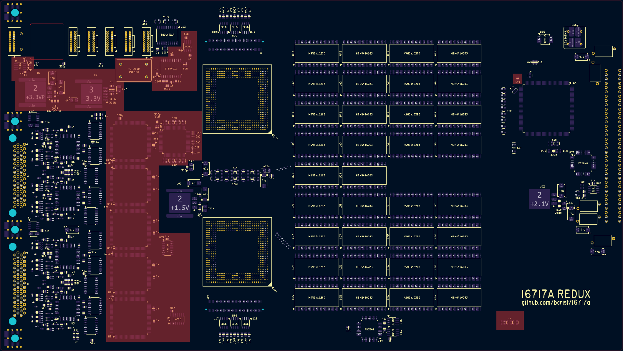
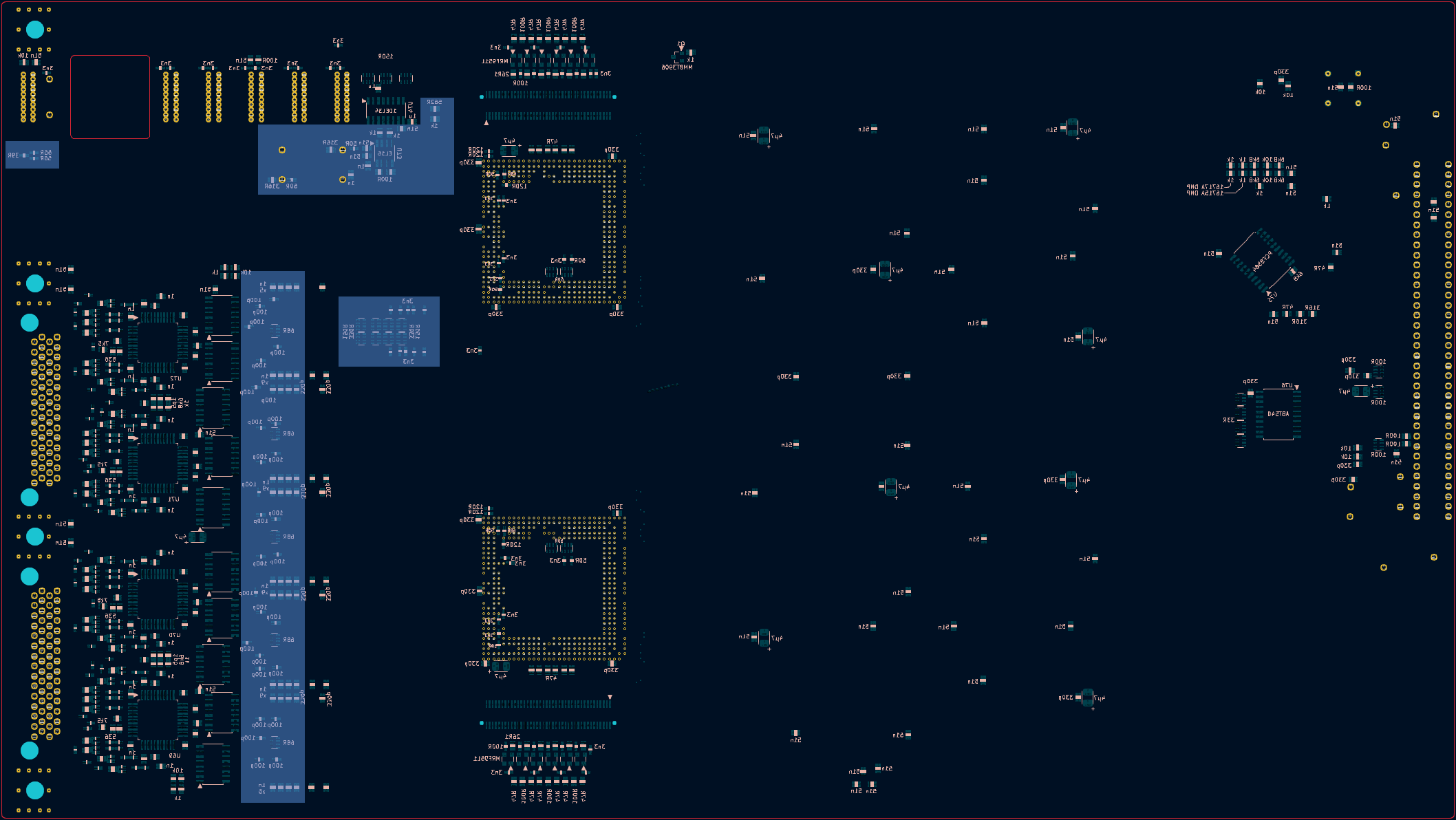
Once everything is complete, cross your fingers and hope that pv shows no failures:
pv> x modtests
Mod   C: TEST passed       # "vramDataTest" (1, 0, 1)
Mod   C: TEST passed       # "vramAddrTest" (1, 0, 1)
Mod   C: TEST passed       # "vramCellTest" (1, 0, 1)
Mod   C: TEST passed       # "vramUnloadTest" (1, 0, 1)
Mod   C: TEST passed       # "chipRegTest" (1, 0, 1)
Mod   C: TEST passed       # "bpClkTest" (1, 0, 1)
Mod   C: TEST passed       # "cmpTest" (1, 0, 1)
Mod   C: TEST passed       # "icrTest" (1, 0, 1)
Mod   C: TEST passed       # "flagTest" (1, 0, 1)
Mod   C: TEST passed       # "armTest" (1, 0, 1)
Mod   C: TEST passed       # "vramSerDataTest" (1, 0, 1)
Mod   C: TEST passed       # "vramSerCellTest" (1, 0, 1)
Mod   C: TEST passed       # "clksTest" (1, 0, 1)
Mod   C: TEST passed       # "calTest" (1, 0, 1)
Mod   C: TEST passed       # "zoomDataTest" (1, 0, 1)
Mod   C: TEST passed       # "zoomMasterTest" (1, 0, 1)
Mod   C: TEST passed       # "fisoRedundancyTest" (1, 0, 1)
Mod   C: TEST passed       # "zoomAcqTest" (1, 0, 1)
Mod   C: TEST passed       # "zoomChipSelTest" (1, 0, 1)
There's only two things left to test now:
pv doesn't report any errors, but something isn't working, it's likely either a faulty comparator chip, a problem with one of the input filtering networks, or a bad probe/cable.pv tests in master configuration before attempting to use them together. If pv reports errors in a multi-card configuration, but not when the boards are all masters, it probably means there's a problem with the circuitry near the board-to-board connectors, or the FFC connectors/cables themselves.Once you're sure a board is fully working, you may want to remove the ASIC heatsinks and reapply them with thermal adhesive rather than regular thermal compound, to avoid the chance of them falling off if the mainframe is moved while the board is inside. If you haven't yet installed the back panel bracket, do that now as well.
I also considered reworking some of the LDOs; in particular the LM2991 which is using +3.3VP as a virtual ground, since the LM2991 can't regulate close to its ground reference. It seems strange that they didn't just use the 3-terminal LM337 instead, since -1.7V shouldn't be a problem for it. The parts do have slightly different noise characteristics, but I can't see that being a problem here, as ECL is pretty tolerant to noise on Vee. In the end, I decided to keep all the LDO circuits as-is, except for some layout adjustments.
| Qty | Value | Footprint | References |
|---|---|---|---|
| 1072 | ~ | fp:TestPoint | TP1, TP10, TP100, TP101, TP1000, TP1001, TP1002, TP1003, TP1004, TP1005, TP1006, TP1007, TP1008, TP1009, TP1010, TP1011 +1056 |
| 124 | 330p NP0 | fp:C0805 | C1005, C1006, C1007, C1008, C1009, C1010, C1011, C1012, C1023, C1024, C1025, C1026, C1027, C1028, C1029, C1030 +108 |
| 96 | 1.1n | fp:C0805 | C1000, C1001, C1013, C1014, C1015, C1016, C1019, C1020, C1021, C1022, C1046, C1047, C1049, C1051, C1052, C1054 +80 |
| 73 | 51n | fp:C0805 | C1003, C1004, C1066, C1072, C1075, C1076, C1077, C1098, C1117, C1119, C1120, C1121, C1122, C1123, C1124, C1130 +57 |
| 68 | ~ | fp:Input Filter_2 | RC1000, RC1001, RC1002, RC1003, RC1004, RC1005, RC1006, RC1007, RC1008, RC1009, RC1010, RC1011, RC1012, RC1013, RC1014, RC1015 +52 |
| 68 | ~ | fp:F0603 | F1000, F1001, F1002, F1003, F1004, F1005, F1006, F1007, F1008, F1009, F1010, F1011, F1012, F1013, F1014, F1015 +52 |
| 68 | ~ | fp:Input Filter | RRC1000, RRC1001, RRC1002, RRC1003, RRC1004, RRC1005, RRC1006, RRC1007, RRC1008, RRC1009, RRC1010, RRC1011, RRC1012, RRC1013, RRC1014, RRC1015 +52 |
| 51 | 3.3n | fp:C0603 | C1002, C1080, C1099, C1101, C1102, C1103, C1191, C1192, C1193, C1194, C1196, C1197, C1198, C1199, C1200, C1201 +35 |
| 39 | 46.4 | fp:R0805 | R1070, R1073, R1074, R1075, R1076, R1077, R1082, R1083, R1084, R1085, R1086, R1088, R1103, R1122, R1127, R1162 +23 |
| 34 | 1k | fp:R0805 | R1014, R1015, R1016, R1017, R1018, R1020, R1032, R1033, R1051, R1067, R1093, R1109, R1123, R1131, R1139, R1140 +18 |
| 34 | MSM5416283 | fp:SSOP-64_10.7x26mm_P0.8mm | U25, U26, U27, U28, U29, U30, U31, U32, U33, U35, U36, U37, U38, U39, U40, U41 +18 |
| 26 | 100 | fp:R0805 | R1039, R1045, R1046, R1052, R1071, R1072, R1078, R1081, R1087, R1089, R1111, R1112, R1113, R1114, R1115, R1116 +10 |
| 23 | 100p | fp:C0603 | C1285, C1286, C1292, C1293, C1298, C1299, C1304, C1310, C1311, C1314, C1315, C1316, C1317, C1318, C1319, C1320 +7 |
| 20 | 4816P-B07-000 | fp:SOIC-16W_5.3x10.2mm_P1.27mm | R125, R126, R127, R128, R129, R130, R131, R132, R133, R134, R328, R329, R330, R331, R333, R334 +4 |
| 18 | 10k | fp:R0805 | R1019, R1021, R1034, R1035, R1092, R1095, R1118, R1119, R1129, R1132, R1134, R1135, R1250, R1251, R1266, R1268 +2 |
| 16 | 51 | fp:R0603 | R1000, R1001, R1060, R1061, R1142, R1149, R1150, R1151, R1156, R1157, R1165, R1166, R1218, R1220, R1223, R1224 |
| 16 | 6.81k | fp:R0805 | R1010, R1011, R1012, R1013, R1062, R1121, R1128, R1130, R1133, R1136, R1137, R1138, R1275, R1276, R1277, R1278 |
| 14 | 100 | fp:R0603 | R1063, R1064, R1159, R1164, R1167, R1180, R1186, R1189, R1192, R1195, R1200, R1210, R1213, R1217 |
| 14 | 4.7u | fp:CP_EIA-3528-21_Kemet-B | C1017, C1018, C1104, C1139, C1141, C1146, C1148, C1167, C1169, C1180, C1183, C1209, C1211, C1345 |
| 12 | 26.1 | fp:R0805 | R1160, R1163, R1171, R1176, R1179, R1185, R1196, R1199, R1203, R1206, R1216, R1222 |
| 12 | 47 | fp:CP_EIA-7343-31_Kemet-D | C1050, C1078, C1079, C1105, C1106, C1108, C1110, C1112, C1114, C1115, C1116, C1118 |
| 12 | MRF9511LT1 | fp:SOT-143 | Q1001, Q1002, Q1003, Q1004, Q1005, Q1006, Q1007, Q1008, Q1009, Q1010, Q1011, Q1012 |
| 10 | 31.6 | fp:R0805 | R1040, R1047, R1053, R1054, R1057, R1231, R1232, R1235, R1238, R1241 |
| 9 | 316 | fp:R0805 | R1043, R1050, R1107, R1124, R1125, R1155, R1158, R1236, R1283 |
| 8 | 1.5p NP0 | fp:C0805 | C1036, C1037, C1042, C1043, C1372, C1373, C1378, C1379 |
| 8 | 100 | fp:SOIC-16W_5.3x10.2mm_P1.27mm | R170, R171, R180, R181, R190, R191, RP17, RP18 |
| 8 | 1NB4-5036 | fp:LQFP-44_10x10mm_P0.8mm | U3, U4, U5, U6, U69, U70, U71, U72 |
| 8 | 33 | fp:SOIC-16W_5.3x10.2mm_P1.27mm | RP4, RP5, RP6, RP7, RP8, RP9, RP10, RP16 |
| 8 | 47 | fp:R_Array_Convex_4x0603 | R1041, R1042, R1048, R1049, R1055, R1056, R1058, R1059 |
| 8 | 536 | fp:R0805 | R1006, R1007, R1008, R1009, R1279, R1280, R1281, R1282 |
| 8 | 7.5k | fp:R0805 | R1002, R1003, R1004, R1005, R1284, R1285, R1286, R1287 |
| 8 | MC100LVEL16 | fp:SOIC-8_3.9x4.9mm_P1.27mm | U1, U17, U18, U19, U20, U23, U24, U73 |
| 6 | 121 | fp:R0603 | R1211, R1212, R1225, R1226, R1227, R1228 |
| 5 | 1NB4-5040 | fp:TQFP-144_20x20mm_P0.5mm | U8, U9, U10, U11, U12 |
| 5 | 68 | fp:R_Array_Convex_4x0603 | R1244, R1245, R1246, R1247, R1248 |
| 5 | ~ | fp:FB_Axial_P12.865mm | L35, L36, L37, L38, L39 |
| 4 | 0.47u | fp:CP_EIA-3528-21_Kemet-B | C1107, C1109, C1111, C1129 |
| 4 | 68 | fp:R0603 | R1036, R1037, R1219, R1221 |
| 3 | 100p NP0 | fp:C0603 | C1082, C1083, C1084 |
| 3 | 150 | fp:SOIC-16W_5.3x10.2mm_P1.27mm | RP1, RP2, RP11 |
| 3 | 51 | fp:SOIC-16W_5.3x10.2mm_P1.27mm | R213, RP12, RP13 |
| 3 | DNP | fp:PinHeader_2x10_P2.54mm_Vertical | J11, J12, J13 |
| 3 | HS | fp:HS | HS2, HS7, HS63 |
| 2 | 1,1n | fp:C0805 | C1048, C1053 |
| 2 | 147 | fp:R0805 | R1242, R1243 |
| 2 | 1821-3936 | fp:BGA-479_40.5mm_P1.27mm | U21, U22 |
| 2 | 1K | fp:R0805 | R1233, R1240 |
| 2 | 215 | fp:R0805 | R1106, R1108 |
| 2 | 330 | fp:SOIC-16W_5.3x10.2mm_P1.27mm | RP14, RP15 |
| 2 | 56 | fp:R0603 | R1290, R1291 |
| 2 | 562 | fp:R0805 | R1230, R1260 |
| 2 | 74LVC08 | fp:SOIC-14_3.9x8.7mm_P1.27mm | U77, U78 |
| 2 | 82 | fp:R0603 | R1065, R1066 |
| 2 | AD586 | fp:SOIC-8_3.9x4.9mm_P1.27mm | U44, U45 |
| 2 | Conn_02x30_Odd_Even | fp:Probe_Connector | J1, J2 |
| 2 | DNP | fp:R0805 | R1038, R1044 |
| 2 | LT1086-ADJ | fp:TO-263-3_TabPin2 | U62, U63 |
| 2 | TPS2011 | fp:SOIC-8_3.9x4.9mm_P1.27mm | S1, S2 |
| 2 | ~ | fp:FB_4x2.7mm | FB1000, FB1001 |
| 2 | ~ | fp:3M_P08-080-SL-A-G_NoHoles | J10, J15 |
| 2 | ~ | fp:3M_P08-080-SL-A-G | J9, J16 |
| 1 | 16715-89002 | fp:PQFP-208_28x28mm_P0.5mm | U64 |
| 1 | 1821-4731 | fp:TQFP-100_14x14mm_P0.5mm | U14 |
| 1 | 1k | fp:SOIC-16W_5.3x10.2mm_P1.27mm | RP3 |
| 1 | 39 | fp:R0603 | R1289 |
| 1 | 74ABT540 | fp:SOIC-20W_7.5x12.8mm_P1.27mm | U76 |
| 1 | 74CBT3125 | fp:SSOP-14_5.3x6.2mm_P0.65mm | U65 |
| 1 | AD7841 | fp:LQFP-44_10x10mm_P0.8mm | U34 |
| 1 | Backplane | fp:AMP_1-534204-4 | J14 |
| 1 | Bracket | fp:Bracket | M1000 |
| 1 | Common | fp:PinHeader_2x10_Horizontal | J3 |
| 1 | DNP | fp:C_Axial_P38.1mm | C176 |
| 1 | Ext+1 | fp:PinHeader_2x10_Vertical | J7 |
| 1 | Ext+2 | fp:PinHeader_2x10_Vertical | J8 |
| 1 | Ext-1 | fp:PinHeader_2x10_Vertical | J5 |
| 1 | Ext-2 | fp:PinHeader_2x10_Vertical | J4 |
| 1 | LM2991 | fp:TO-263-5_TabPin3 | U2 |
| 1 | LM311 | fp:SOIC-8_3.9x4.9mm_P1.27mm | U16 |
| 1 | LT1086-CM | fp:TO-263-3_TabPin2 | U7 |
| 1 | MC100LVEL11 | fp:SOIC-8_3.9x4.9mm_P1.27mm | U68 |
The 2,092 most common of 2,101 parts.
bcrist/16717a
I would not recommend attempting to build one of these boards unless you have and know how to use the following equiment:

bcrist/16717a
I would not recommend attempting to build one of these boards unless you have and know how to use the following equiment:

ereisch/Data_East_PS
Data East pinball power supply board, replacement for 520-5047-02


ifilot/p2000t-teletekst-cartridge
Teletekst interfacing cartridge for the P2000T

jfryman/mw-cart
MegaWiFi Mega Drive/Genesis Wi-Fi cartridge — Rev.C fork (TI TL16C550D UART, 20 MHz / 1.25 Mbaud). Upstream: gitlab.com/doragasu/mw-cart

roberto314/EVA-1_Reproduction
Recreation of the very rare K-K Systems EVA-1 Display Adapter for the Epson HX-20 Computer

kysilv/z80-rp2350b-zx-compatible
Retrocomputer compatible with ZX Spectrum based on real Z80 + discrete RAM/ROM + rp2350b as ULA

roberto314/Unicomp2
A modular 8-bit Computer able to recreate (nearly) every Retro computer of the late 70s to mid 80s.
It measures 365.8 × 205 mm and has 8 copper layers, 1.63 mm thick.
2,101 parts, built around the MC100LVEL16D, AD7841AS, MC100LVEL11D and 74LVC08AD. The full list of its parts is on this page, with links to each part's symbol and footprint where PCBKit's library has them.
From the bcrist/16717a repository on GitHub, at the commit this page was made from: the board is original/original.kicad_pcb and its schematic bga_stencil/bga_stencil.kicad_sch. PCBKit opens the board in the browser, with nothing to install.
Its repository states no licence, so its author keeps all rights: ask bcrist before reusing the design.