
2 layers65 × 55 mm
 batteringramattack/batteringram41
Artifact for "Battering RAM: Low-Cost Interposer Attacks on Confidential Computing via Dynamic Memory Aliasing"
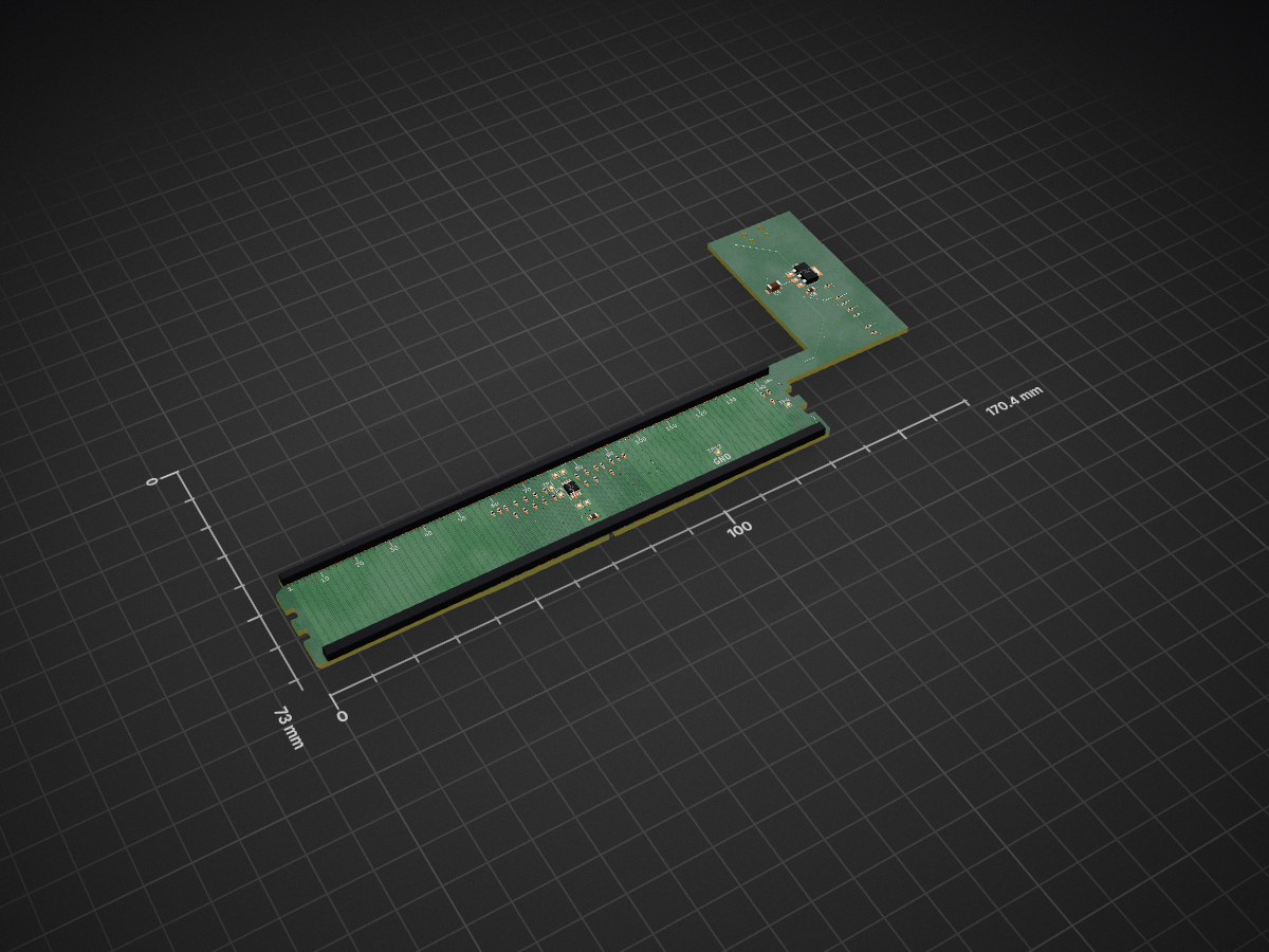
Fault injector is an open-source printed circuit board by batteringramattack, from the batteringramattack/batteringram repository on GitHub, published under the MIT licence. It is a 4-layer board of 170.4 × 73 mm with 88 parts on 244 nets, routed with 1,091 tracks and 259 vias.
It is built around the ADG902BRMZ. Its parts include 12 resistors, 9 capacitors, 9 ICs and 2 connectors. It belongs with the RP2040 boards of this library.
This directory contains the schematics and PCB layout (KiCad) of the Battering RAM interposer.
The interposer is configurable: it has several footprints for analog switches, of which only a few are populated, depending on which address lines you want to manipulate. The sections below describe which parts are always required, which depend on the configuration, and the configurations we used in the paper.
| Description | Reference | Part number | Populate |
|---|---|---|---|
| DDR4 DIMM connector | J2 | CONN-DDR4-288-SM | Always |
| Raspberry Pi Pico 2 | U3 | Raspberry Pi Pico 2 | Always |
| Voltage regulator, 2.5 V | U8 | LD1117S25TR | Always |
| Capacitor, 1206, 10 µF | C9 | Always | |
| Capacitor, 0603, 100 nF | C8 | Always | |
| Analog switch | U1, U2, U4–U7, U9 | ADG902BRMZ | Per configuration |
| Resistor, 0402, 1 kΩ | R1–R7 | Per configuration | |
| Capacitor, 0603, 100 nF | C1–C7 | Per configuration | |
| Jumper, 0402, 0 Ω | R8, R9, R11, R13, R17 | Per configuration |
The interposer has seven switch positions:
Axx -> Axx on the silkscreen.Axx -> A17 on the silkscreen. To connect the switch output to the DIMM, the output jumper must be populated.Each switch has its own pull-up resistor and decoupling capacitor. Each in-line switch also has a passthrough jumper that connects the line directly when the switch is not populated.
| Switch | CPU-side line | DIMM-side line | Passthrough jumper | Pull-up | Decoupling cap | Output Jumper |
|---|---|---|---|---|---|---|
| U4 | A11 | A11 | R11 | R4 | C2 | - |
| U1 | A13 | A13 | R13 | R1 | C3 | - |
| U6 | A17 | A17 | R17 | R5 | C5 | - |
| U5 | A11 | A17 | – | R3 | C4 | R8 |
| U2 | A13 | A17 | – | R2 | C1 | R9 |
| U7 | TP2 / TP11 | TP6 / TP12 | – | R6 | C6 | - |
| U9 | TP8 / TP9 | TP7 / TP10 | – | R7 | C7 | - |
Each populated switch needs a pull-up resistor (1 kΩ) and a 100 nF decoupling capacitor, see the table above. In-line switches (U4, U1, U6) that are left unpopulated need their passthrough jumper instead, otherwise the corresponding address line is not connected to the DIMM. The exception is A17 when one of the redirect switches (U5, U2) is installed: the redirect switch then drives A17, so R17 is left unpopulated.
[!NOTE] Each DIMM-side line must be driven by exactly one path: its in-line switch, its passthrough jumper, or (for A17) one of the redirect switches. For example, populating both U5 (A11 -> A17) and U6 (A17 -> A17), or U2 (A13 -> A17) together with R17, is invalid, as both would drive A17 on the DIMM.
Besides the switch positions, many other signals pass through 0402 jumper footprints (JP1–JP20 and JP23–JP43) that are bridged on the PCB by default. This includes most of the CA bus (all address lines except A11, A13 and A17, which go through the switch positions), the clock, reset and chip-select lines, among others. These signals work as-is without populating anything.
To manipulate one of these signals, cut the bridge between the jumper pads to interrupt the line, and wire the two pads to one of the general-purpose switches (U7, U9). To restore the original connection later, simply solder a 0402 0 Ω resistor onto the footprint.
| Populate | Passthrough jumpers |
|---|---|
| U1 (A13 -> A13) with R1, C3 | R11, R17 |
| Populate | Passthrough jumpers |
|---|---|
| U1 (A13 -> A13) with R1, C3 | R11 |
| U2 (A13 -> A17) with R2, C1, R9 |
| Populate | Passthrough jumpers |
|---|---|
| U4 (A11 -> A11) with R4, C2 | R17 |
| U1 (A13 -> A13) with R1, C3 |
Recommended settings when ordering the PCB:
[!NOTE] 1.6 mm is slightly thicker than regular DDR4 memory modules (1.4 mm). To avoid damaging the motherboard's DIMM socket, it is recommended to use a DDR4 DIMM extender between the motherboard and the interposer.
| Qty | Value | Footprint | References |
|---|---|---|---|
| 41 | Jumper_2_Bridged | badram:Jumper_0402_bridged | JP1, JP2, JP10, JP11, JP12, JP13, JP14, JP15, JP16, JP17, JP18, JP19, JP20, JP23, JP24, JP25 +25 |
| 15 | TestPoint | TestPoint:TestPoint_Pad_1.0x1.0mm | TP1, TP2, TP3, TP4, TP5, TP6, TP7, TP8, TP9, TP10, TP11, TP12, TP13, TP14, TP15 |
| 7 | 1k | Resistor_SMD:R_0402_1005Metric_Pad0.72x0.64mm_HandSolder | R1, R2, R3, R4, R5, R6, R7 |
| 7 | ADG902BRMZ | Package_SO:MSOP-8_3x3mm_P0.65mm | U1, U2, U4, U5, U6, U7, U9 |
| 7 | C_Small | Capacitor_SMD:C_0603_1608Metric_Pad1.08x0.95mm_HandSolder | C1, C2, C3, C4, C5, C6, C7 |
| 3 | 0R | Resistor_SMD:R_0402_1005Metric_Pad0.72x0.64mm_HandSolder | R11, R13, R17 |
| 2 | 0 | Resistor_SMD:R_0402_1005Metric_Pad0.72x0.64mm_HandSolder | R8, R9 |
| 1 | 100nF | Capacitor_SMD:C_0603_1608Metric_Pad1.08x0.95mm_HandSolder | C8 |
| 1 | 10uF | Capacitor_SMD:C_1206_3216Metric_Pad1.33x1.80mm_HandSolder | C9 |
| 1 | DDR4_to_DIMM | badram:ddr4-edge-conn-female-badram | J2 |
| 1 | DDR4_to_MB | fi-library:ddr4-edge-conn-male | J1 |
| 1 | LD1117S25TR_SOT223 | Package_TO_SOT_SMD:SOT-223-3_TabPin2 | U8 |
| 1 | Pico | badram:RPi_Pico_SMD_TH | U3 |
It measures 170.4 × 73 mm and has 4 copper layers, 1.6 mm thick.
88 parts, built around the ADG902BRMZ. The full list of its parts is on this page, with links to each part's symbol and footprint where PCBKit's library has them.
From the batteringramattack/batteringram repository on GitHub, at the commit this page was made from: the board is ddr4-interposer/fault-injector.kicad_pcb and its schematic ddr4-interposer/dimm-conn.kicad_sch. PCBKit opens the board in the browser, with nothing to install.
Its repository publishes it under the MIT licence: you may reuse it on that licence's terms (keep the author's notice, and for a copyleft licence share your changes alike).


conol-ai/openmicrokbd
Open-source recreation of OpenAI's Codex Micro macropad — PCB written in CoHDL, an AI-native hardware description language. Rust firmware (embassy) + companion app (makepad). MIT licensed. https://openmicrokbd.org


curtisseizert/Nanovoltmeter
A low noise nanovoltmeter design files and code


qwertpas/O32controller
Miniature closed-loop controller for brushless DC motors