6 layers90 × 94.5 mm
Fpga stm32-ifaces
azonenberg/misc-devboards
Miscellaneous prototype hardware that wasn't major enough to warrant a dedicated repo
274 parts17BSD-3-Clause
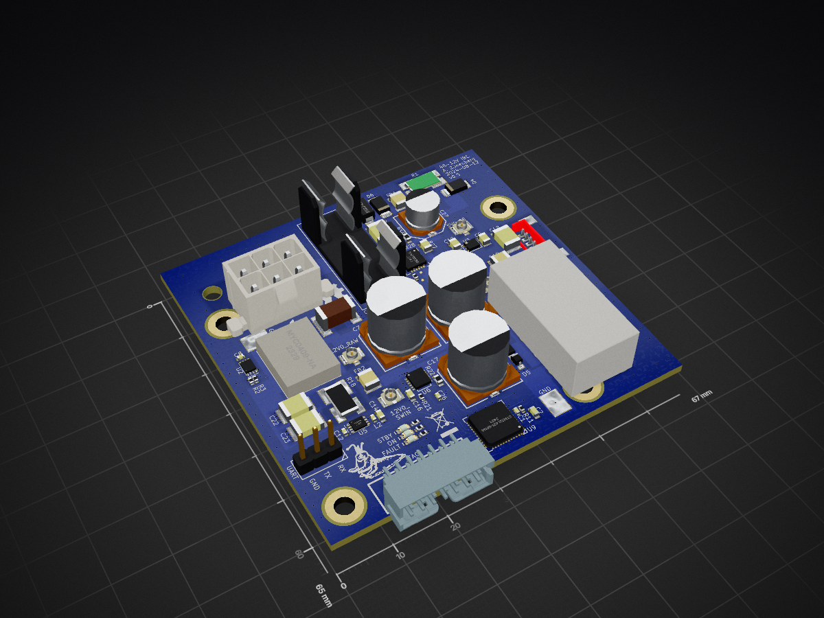
 azonenberg/common-ibc6
48-12V 72W intermediate bus converter common to all of my larger FPGA projects
Common ibc is an open-source printed circuit board by azonenberg, from the azonenberg/common-ibc repository on GitHub, published under the BSD-3-Clause licence. It is a 4-layer board of 67 × 65 mm with 112 parts on 82 nets, routed with 896 tracks and 468 vias.
It is built around the MUN12AD03-SE, MYC0409-NA and 74LVC1G08Z, with the NCP45560IMNTWG-H, TPS16630PWP and BLE32SN120BN1L among its other parts. Its parts include 38 resistors, 28 capacitors, 11 connectors, 10 ICs and 7 diodes. It belongs with the fPGA and programmable logic boards and the STM32 boards of this library.


This is a 48-12V 72W non-isolated intermediate bus converter which I plan to use in all of my larger FPGA projects.
It uses a charge pump which has a fixed divide-by-4 output ratio rather than using a regulating buck topology. This allows high efficiency but requires downstream loads to be able to tolerate a wider range of input voltages.
The architecture is scalable to 2 or 4 parallel converter modules, allowing 144W (12A) or 288W (24A) IBCs based on the same chipset to be constructed in a straightforward manner based on a scaling of this design, however there are no near-term plans to create such a converter since none of my near term project plans require that much power.
The input is +48VDC nominal on a 6-pin Molex Mini-Fit Jr connector, using a pinout compatible with the Mean Well GST280A48-C6P power brick (and possibly others). The negative terminal of the input power connection is connected to circuit ground.
The permissible operating range is 40 to 56VDC (corresponding to 10 to 14V output). An input protection circuit will disable the converter if the input is out of this range.
The unregulated output voltage is 1/4 of the input, so if the load has tighter requirements for accuracy of the 12V rail then this will further constrain the input supply voltage.
The converter is built around the Murata MYC0409-NA charge pump DC-DC module.
In addition to the high current 12V output (on an 8-pin Molex Mini-Fit Jr connector) the converter provides a 3.3V standby rail (using the Cyntec MUN12AD03-SE regulating off of the 12V rail), capable of up to 3A, which is intended for powering sleep/idle circuitry such as soft power on/off, rail sequencing, etc.
Both the primary 12V step-down converter and the 3.3V standby regulator are always enabled, however a load switch on the main 12V output allows it to be disabled to completely power down the bulk of the downstream device, keeping only the converter board and the 3V3_SB rail on the downstream device energized. The load switch has an integrated soft start, preventing high current surges when charging bulk capacitance on the load.
The onboard STM32L431 microcontroller monitors the PGOOD signals of internal regulators as well as the ALERT output of the onboard AT30TS74 temperature sensor. It also continually uses an internal ADC to record the input and output voltage, downstream load sense voltage, and input and output current. All of these sensor readings may be queried by the load over the I2C management bus.
The converter includes multiple levels of protection to minimize the risk of fire or equipment damage.
The most critical interlocks are implemented in hardware while additional protections with lower thresholds are implemented in software on the management MCU.
If a software interlock triggers, the 12V output is disabled. The management MCU will automatically attempt to restart the output (as long as the load is still requesting power) at periodic intervals once the fault condition is cleared.
The 3.3V standby output will remain active and the management MCU will remain operational while a software interlock is tripped.
The 48V input is fused at 2.5A using a socketed 5x20mm fast-blow fuse.
The 12V primary output is fused at 10A using a soldered-down fast-blow fuse.
The 3.3V standby output is current limited (typical range 3.8 - 5.2A) by the DC-DC converter and does not have an supplemental fuse.
If the 12V output current exceeds 6.5A, a software interlock is triggered. The output load switch also has a short circuit protection feature, however the software interlock is intended to trip at a lower level.
If any of the internal regulators indicates a problem (PGOOD low) a software interlock is triggered.
If the AT30TS74 indicates an out-of-bounds temperature (ALERT low) a software interlock is triggered.
The MCU does not configure the AT30TS74; on power up the default over-temperature limit (80C) is active. This sensor is located on the same I2C management bus as the MCU and may be reconfigured or queried by the load as required; the IBC will activate the interlock if the programmed temperature range is exceeded.
The input is monitored by a TPS16630 protection controller, which also provides soft-start for the input bulk capacitance. If the input voltage drops below 40V or rises above 56V (corresponding to 10-14V output) the system will shut down completely (input power cut off upstream of the charge pump, disabling the microcontroller, 3.3V standby rail, and all internal circuitry past the protection controller).
The input has a Schottky diode to ground in reverse polarity. If the input goes significantly negative (reverse polarity connection) the diode will conduct and blow the input fuse, hopefully protecting the load and possibly even the power supply from damage.
As an additional protection against catastrophic overvoltage at the input, a zener clamp will trip at approximately 58V, blowing the input fuse.
Since the output voltage is normally a fixed 4:1 scaling of the input, output voltage drifting beyond this range is likely indicative of a failure of the charge pump module.
| Qty | Value | Footprint | References |
|---|---|---|---|
| 9 | 0.47 uF | azonenberg_pcb:EIA_0402_CAP_NOSILK | C3, C4, C5, C8, C11, C12, C15, C25, C26 |
| 7 | 10K | azonenberg_pcb:EIA_0402_RES_NOSILK | R4, R15, R21, R24, R25, R26, R31 |
| 5 | U.FL | azonenberg_pcb:CONN_U.FL_TE_1909763-1 | J6, J7, J8, J9, J10 |
| 4 | SCREWHOLE | azonenberg_pcb:MECHANICAL_CLEARANCEHOLE_4_40 | MH1, MH2, MH3, MH4 |
| 3 | 1K | azonenberg_pcb:EIA_0402_RES_NOSILK | R8, R9, R32 |
| 3 | 4.7 uF | azonenberg_pcb:EIA_0603_CAP_NOSILK | C2, C13, C14 |
| 3 | 470 | azonenberg_pcb:EIA_0402_RES_NOSILK | R16, R17, R23 |
| 3 | DNP | azonenberg_pcb:EIA_0402_RES_NOSILK | R11, R35, R37 |
| 2 | 2.2 uF | azonenberg_pcb:EIA_0805_CAP_NOSILK | C9, C10 |
| 2 | 22 uF | azonenberg_pcb:EIA_1210_CAP_NOSILK | C19, C20 |
| 2 | 22 uF 25V | azonenberg_pcb:EIA_1812_CAP_NOSILK | C22, C23 |
| 2 | 33K | azonenberg_pcb:EIA_0402_RES_NOSILK | R10, R13 |
| 2 | 4.7K | azonenberg_pcb:EIA_0402_RES_NOSILK | R2, R3 |
| 2 | 62 nH | azonenberg_pcb:EIA_0402_CAP_NOSILK | L1, L2 |
| 2 | 8.06K | azonenberg_pcb:EIA_0402_RES_NOSILK | R12, R14 |
| 2 | AD8218 | azonenberg_pcb:DFN_8_0.5MM_2x3MM_TALL | U4, U5 |
| 2 | BLE32SN120BN1L | azonenberg_pcb:EIA_1210_CAP_NOSILK | FB1, FB2 |
| 2 | EEH-ZU1J101V | azonenberg_pcb:CAP_AL_10MM_SMT | C6, C7 |
| 2 | GREEN | azonenberg_pcb:EIA_0603_LED | D1, D2 |
| 2 | GROUND | azonenberg_pcb:TESTPOINT_SMT_KEYSTONE_5016 | J3, J4 |
| 2 | PTVS58VP1UP,115 | azonenberg_pcb:SOD128 | D4, D6 |
| 2 | TESTPOINT | azonenberg_pcb:TESTPOINT_SMT_0.5MM | TP2, TP3 |
| 1 | 0.015 uF | azonenberg_pcb:EIA_0603_CAP_NOSILK | C16 |
| 1 | 0.1 uF | azonenberg_pcb:EIA_0402_CAP_NOSILK | C1 |
| 1 | 1.33K | azonenberg_pcb:EIA_0402_RES_NOSILK | R6 |
| 1 | 10 nF | azonenberg_pcb:EIA_0402_CAP_NOSILK | C28 |
| 1 | 100k | azonenberg_pcb:EIA_0402_RES_NOSILK | R19 |
| 1 | 10A | azonenberg_pcb:EIA_1206_FUSE_NOSILK | F2 |
| 1 | 17.8K | azonenberg_pcb:EIA_0402_RES_NOSILK | R38 |
| 1 | 20K | azonenberg_pcb:EIA_0402_RES_NOSILK | R34 |
| 1 | 22 uF | azonenberg_pcb:EIA_1812_CAP_NOSILK | C18 |
| 1 | 22.1k | azonenberg_pcb:EIA_0402_RES_NOSILK | R20 |
| 1 | 25SVPF330M | azonenberg_pcb:CAP_AL_10MM_SMT | C17 |
| 1 | 33 | azonenberg_pcb:EIA_0402_RES_NOSILK | R7 |
| 1 | 39K | azonenberg_pcb:EIA_0402_RES_NOSILK | R5 |
| 1 | 4.7 uF 100V | azonenberg_pcb:CAP_TDK_CKG57K | C21 |
| 1 | 470 1/4W | azonenberg_pcb:EIA_0603_RES_NOSILK | R22 |
| 1 | 5x20 2.5A | azonenberg_pcb:FUSEHOLDER_KEYSTONE_4527 | F1 |
| 1 | 6.49K | azonenberg_pcb:EIA_0402_RES_NOSILK | R30 |
| 1 | 620 | azonenberg_pcb:EIA_0402_RES_NOSILK | R29 |
| 1 | 74LVC1G08 | azonenberg_pcb:DFN_6_0.5MM_1.4x1.00MM_NXP_X2-DFN1410-6 | U10 |
| 1 | 806K | azonenberg_pcb:EIA_0603_RES_NOSILK | R28 |
| 1 | 875105945001 | azonenberg_pcb:CAP_AL_6.3MM_SMT | C27 |
| 1 | 9.09K | azonenberg_pcb:EIA_0402_RES_NOSILK | R33 |
| 1 | AT30TS74_UDFN | azonenberg_pcb:DFN_8_0.5MM_2x3MM_TALL | U2 |
| 1 | CONN_01X03 | azonenberg_pcb:CONN_HEADER_2.54MM_1x3 | TP1 |
| 1 | CUHZ16V,H3F | azonenberg_pcb:SOD323H | D5 |
| 1 | DNP | azonenberg_pcb:EIA_0603_RES_NOSILK | R36 |
| 1 | DNP | azonenberg_pcb:EIA_0805_CAP_NOSILK | R27 |
| 1 | ES2J-LTP | azonenberg_pcb:SMA | D7 |
| 1 | GA343DR7GD472KW01L | azonenberg_pcb:EIA_1812_CAP_NOSILK | C24 |
| 1 | LOGO | w_logo:Logo_silk_OSHW_6x6mm | M2 |
| 1 | LOGO | w_logo:Logo_silk_WEEE_3.4x5mm | M4 |
| 1 | LOGO | azonenberg_pcb:LONGTHING-1200DPI | M1 |
| 1 | LOGO | w_logo:Logo_silk_ROHS_5x2.8mm | M3 |
| 1 | LVK24R025DER | azonenberg_pcb:OHMITE_LVK24 | R1 |
| 1 | LVK25R005FER | azonenberg_pcb:OHMITE_LVK25 | R18 |
| 1 | MI0603J601R-10 | azonenberg_pcb:EIA_0603_INDUCTOR_NOSILK | FB3 |
| 1 | MOLEX_0039291067 | azonenberg_pcb:CONN_MOLEX_MINIFITJR_6POS_0039291067 | J2 |
| 1 | MOLEX_0039291087 | azonenberg_pcb:CONN_MOLEX_MINIFITJR_8POS_0039291087 | J11 |
| 1 | MOLEX_0532610571 | azonenberg_pcb:CONN_MOLEX_PICOBLADE_5POS_0532610571 | J5 |
| 1 | MUN12AD03-SE | azonenberg_pcb:MODULE_CYNTEC_MUN12AD03-SE | U7 |
| 1 | MYC0409-NA | azonenberg_pcb:MODULE_MURATA_MYC0409-NA | U8 |
| 1 | NCP45560IMNTWG-H | azonenberg_pcb:DFN_12_0.5MM_3x3MM | U6 |
| 1 | RED | azonenberg_pcb:EIA_0603_LED | D3 |
| 1 | STM32L431-QFN48 | azonenberg_pcb:QFN_48_0.5MM_7x7MM | U9 |
| 1 | TPS16630 | azonenberg_pcb:QFN_24_0.5MM_4x4MM | U1 |
| 1 | TPS7A2550DRVR | azonenberg_pcb:DFN_6_0.65MM_2x2MM | U3 |
| 1 | XILINX_JTAG | azonenberg_pcb:XILINX_JTAG_PTH_MOLEX_0878311420 | J1 |
It measures 67 × 65 mm and has 4 copper layers, 1.6 mm thick.
112 parts, built around the MUN12AD03-SE, MYC0409-NA, 74LVC1G08Z and NCP45560IMNTWG-H. The full list of its parts is on this page, with links to each part's symbol and footprint where PCBKit's library has them.
From the azonenberg/common-ibc repository on GitHub, at the commit this page was made from: the board is pcb/common-ibc.kicad_pcb and its schematic pcb/common-ibc.kicad_sch. PCBKit opens the board in the browser, with nothing to install.
Its repository publishes it under the BSD-3-Clause licence: you may reuse it on that licence's terms (keep the author's notice, and for a copyleft licence share your changes alike).
azonenberg/misc-devboards
Miscellaneous prototype hardware that wasn't major enough to warrant a dedicated repo

azonenberg/latentred
Open hardware 48x 1000baseT + 2x 25G SFP28 Ethernet switch

azonenberg/triggercrossbar
Rack mountable crossbar matrix for T&M trigger in/out signals, allowing dynamic reconfiguration of an experiment without recabling


jagdeepsingh02/ENNOID-Dual-Gate-Driver
Dual Gate Driver for IGBT or Mosfet modules

misko/prompt2device
The separate vNext PCB skill and orchestrator package is available alongside the reference workflow below; existing projects keep their accepted toolchain until an explicit migration.