2 layers32 × 20 mm
 awong-dev/pager
Low-powered, gps and messaging capable pager for kids
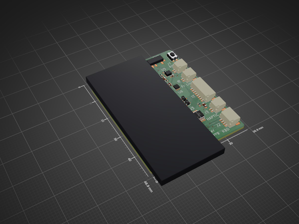
Pager carrier is an open-source printed circuit board by awong-dev, from the awong-dev/pager repository on GitHub. It is a 2-layer board of 38.9 × 48.9 mm with 79 parts on 83 nets, routed with 1,023 tracks and 69 vias.
It is built around the SN74LVC2G126DCUR, CP2102N-A02-GQFN24 and TPS62840DLCR, with the BQ25185DLHR, LIS2DW12TR-MS and MAX17048G+T10 among its other parts. Its parts include 36 resistors, 19 capacitors, 8 connectors, 7 ICs and 4 transistors.


KiCad 10 projects for the carrier board that replaces the Adafruit breakouts
around the Walter module, and for the small panel board that drives the
2.9" SSD1680 e-ink glass. Both started as Python under gen/.
Carrier: hand-edited since 19 Oct 2026 (commit "Manually review and fix
carrier board schematic"). The carrier .kicad_sch files are the source of
truth; gen/carrier.py / gen/carrier_pcb.py / gen/build.py describe the
17 Oct version and must NOT be re-run (they overwrite the hand edits). The
carrier .kicad_pcb still matches the 17 Oct netlist and needs "Update PCB
from schematic" after the schematic rework.
Panel: still generated. gen/panel.py + gen/panel_pcb.py are current;
regenerate only the panel with a driver that calls build.build_panel(True)
(never build.py's main, which rebuilds the carrier too), then
panel_pcb.py --route and finish_pcb.py panel with KiCad's python.
Brief: the "Pager Carrier Board — KiCad Handoff" doc (17 Oct 2026). The owner added two changes on 17 Oct: the fuel gauge is populated, and the e-ink ZIF and boost cluster moved to a separate panel board that sits between the glass and the battery, cabled to the carrier over an 8-way JST SH.
| Path | What |
|---|---|
pager-carrier.kicad_pro/.kicad_sch/.kicad_pcb | carrier project, root schematic, board |
power.kicad_sch … peripherals.kicad_sch | the five hierarchical sheets from the brief |
pager-carrier.kicad_sym, pager-carrier.pretty/ | project symbols (Walter, BQ25185, TPS62840, LIS2DW12, DRV2605L, MAX17048, rail power symbols) and custom footprints (Walter, BQ25185, TPS62840, USB4235, FH34SRJ 24S/6S) |
panel/ | pager-panel project (display ZIF, front-light ZIF, boost, 10-way SH), shares the symbol library above |
out/, panel/out/ | ERC and DRC reports, schematic PDF, BOM CSV, netlist, Freerouting DSN/SES |
gen/ | generator: build.py (schematics + exports), carrier_pcb.py / panel_pcb.py (boards, run with KiCad's python), finish_pcb.py |
Regenerate: python3 gen/build.py (schematics, ERC, PDF, BOM, netlist), then
/Applications/KiCad/KiCad.app/Contents/Frameworks/Python.framework/Versions/Current/bin/python3 gen/carrier_pcb.py --route
(needs the Freerouting jar path in gen/pcb.py) and the same for panel_pcb.py.
Walter_Module_2x14_THT: datasheet rev 1.1 (hw 1.6) section 6 plus the
vendor walter-solder.kicad_mod in ~/src/walter-hardware. Rows 17.78 mm
apart, 2.54 pitch, pin 1 at 9.72 mm from the USB-C end, 1.02 drill / 1.7 pad.
The carrier sits above a header-side-up Walter, so the pattern is the
mirror of the vendor's: pin 1 is on the +X row as seen from the carrier
top. SIM holder, u.FL jacks and USB-C are marked on User.Comments.BQ25185_WSON-10_DLH0010A_2.2x2mm_P0.4mm_EP0.9x1.5mm: TI drawing 4226298/A
(datasheet SLUSF65B): pads 0.5 x 0.2 on 0.4 pitch, columns 2.1 mm apart,
thermal pad 0.9 x 1.5 with two 0.2 mm vias. Matches the SnapEDA footprint in
~/Documents/KiCad/KidPager/BQ25185DLHR/ and KiCad's stock
Texas_DLH0010A_WSON-10-1EP_2.2x2mm_P0.4mm_EP0.9x1.5mm pad for pad.USB_C_Receptacle_GCT_USB4235_Vertical: GCT drawing rev A (21 Aug 2024).
16 pads 0.30 x 0.87 on 0.5 pitch at x = ±0.25/0.75/1.25/2.75, rows at
y = ±0.87; plated shell slots 0.6 x 0.85 (1.1 x 1.35 copper) at x = ±5.0; NPTH
pegs 0.6 mm at x = ±3.75. Height 6.5 mm. Only ordering code: USB4235-03-C.TPS62840_VSON-HR-8_DLC0008B_1.5x2mm_P0.5mm: TI DLC0008B land pattern, pads
0.6 x 0.25 at x = ±0.65 (the stock SOT-583-8 is 0.09 mm wider per side).Hirose_FH34SRJ-24S-0.5SH and -6S-: Hirose FH34SRJ catalog (Nov 2018)
page 4 land pattern: contact pads 0.3 x 0.8 on 0.5 pitch, fitting pads
0.4 x 0.8 at the E/F spans 3.3 mm behind the contacts; body D wide, 3.8 deep,
1.0 mm high, top and bottom contact, back-flip actuator. Pin 1 at -X with
the contacts (FPC entry) at -Y, the same convention as KiCad's FH12 footprints.
KiCad 10 ships no FH34SRJ footprints.| Part | Height above its board |
|---|---|
| J1 USB4235 vertical USB-C | 6.5 mm (owner's choice; the horizontal fallback is 3.2) |
| J2, J4 JST PH side-entry (S2B/S4B-PH-SM4-TB) | 5.5 mm (6.0 deep; JST ePH catalog p.4) |
| SW1 slide switch JS102011SAQN | 3.5 mm |
| J3 JST SH side-entry SM10B-SRSS-TB | 2.9 mm |
| SW2 tactile SKQGAFE010 | 1.5 mm (sits beside the glass, below the glass top) |
| everything under the glass | ≤ 1.3 mm: 0805 caps 1.25, SOT-23 1.1, QFN 0.9, L2 1.0 (the 1210 100 µF at 2.5 mm is gone) |
| glass GDEY029T94-FL03 | 2.01 mm incl. the front-light plate |
| panel board | 1.0 mm FR4 + 1.5 mm (L1) ; FH34SRJ ZIFs 1.0, SOD-123 1.1 — a 0.8 mm board is fine |
So above the carrier: glass stack ≈ 1.3 + 2.0 (or panel 1.0 + 1.5 + 2.0 at the tail end), and the USB-C at 6.5 is the only thing taller than 3.5 mm.
pins.h entry for it.TDFN-8-1EP_2x2mm_P0.5mm_EP0.8x1.2mm
(matches the Maxim 21-0168 drawing); DRV2605L uses TSSOP-10_3x3mm_P0.5mm
(TI DGS land within 0.05 mm).Battery only, SW1 on, Walter asleep. Carrier parts, from the datasheets:
| Consumer | Sleep current | Note |
|---|---|---|
| BQ25185 battery quiescent (IQ_BAT) | 4 µA typ, 5 max | unavoidable while the cell is connected |
| MAX17048 | 3 µA hibernate (23 µA active) | firmware must leave HIBRT at its default so it auto-hibernates, or force hibernate |
| TPS62840 3V3 buck | ~0.1 µA (36 nA VIN + 56 nA VOS) | |
| TPS22917 (3V3_EPD off) | 10 nA | 0.5 µA when on |
| LIS2DW12 low-power mode 1 | ~1 µA | shake wake; 50 nA if powered down |
| Q1 gate network | 1.9 µA (was 38 µA) | 100 k pull-up changed to 2.2 M; the ON switch pulls the gate low through 10 k + pull-up |
| SN74LVC2G126 U6 | 0 (was up to ~10 µA) | VCC moved from 3V3 to BRG_VDD (CP2102N regulator), so it is unpowered without USB; Ioff outputs, ESP_RX0 held by its 10 k |
| CP2102N | 0 | bus powered |
| STAT/ACC/RX0/FL_BTN pull-ups, VBUS dividers | 0 | all idle high or on VBUS |
| front light, Q4, keyboard rail, panel rail | 0 | switched off |
Carrier total ≈ 10 µA on top of the Walter's own deep-sleep draw. Nothing else on the carrier is worth a part swap; the fuel gauge is the biggest remaining item and it is the one the owner asked to keep.
No. Every TPS6284x orderable (TPS62840 1.8–3.3 V, TPS62841 0.8–1.55 V, TPS62842 1.8–3.6 V; DLC, YBG and DGR packages) sets its output with the VSET resistor; there is no fixed-3.3 V code. The 267 k 0603 stays.
| Qty | Value | Footprint | References |
|---|---|---|---|
| 8 | 100nF | pager-carrier:C_0402_1005Metric_NoSilk | C2, C3, C5, C9, C12, C14, C17, C18 |
| 7 | 10k | pager-carrier:R_0402_1005Metric_NoSilk | R7, R8, R14, R24, R26, R28, R30 |
| 6 | 100k | pager-carrier:R_0402_1005Metric_NoSilk | R4, R5, R6, R10, R34, R37 |
| 4 | 4.7k | pager-carrier:R_0402_1005Metric_NoSilk | R15, R16, R17, R18 |
| 3 | 0R | pager-carrier:R_0402_1005Metric_NoSilk | R11, R23, R39 |
| 3 | 10uF | pager-carrier:C_0402_1005Metric_NoSilk | C15, C16, C19 |
| 2 | 100uF | Capacitor_SMD:C_0805_2012Metric | C6, C7 |
| 2 | 1M | pager-carrier:R_0402_1005Metric_NoSilk | R22, R32 |
| 2 | 1k | pager-carrier:R_0402_1005Metric_NoSilk | R3, R9 |
| 2 | 1uF | pager-carrier:C_0402_1005Metric_NoSilk | C10, C11 |
| 2 | 220R | pager-carrier:R_0402_1005Metric_NoSilk | R19, R20 |
| 2 | 5.1k | pager-carrier:R_0402_1005Metric_NoSilk | R29, R31 |
| 1 | 10uF | Capacitor_SMD:C_0603_1608Metric | C8 |
| 1 | 15R | Resistor_SMD:R_0603_1608Metric | R12 |
| 1 | 18k | pager-carrier:R_0402_1005Metric_NoSilk | R25 |
| 1 | 1uF/25V | Capacitor_SMD:C_0603_1608Metric | C13 |
| 1 | 2.2uH | pager-carrier:L_Murata_DFE201610P_NoSilk | L1 |
| 1 | 22k | pager-carrier:R_0402_1005Metric_NoSilk | R1 |
| 1 | 267k | pager-carrier:R_0402_1005Metric_NoSilk | R38 |
| 1 | 330R | pager-carrier:R_0402_1005Metric_NoSilk | R21 |
| 1 | 4.7uF | Capacitor_SMD:C_0603_1608Metric | C1 |
| 1 | 4.7uF | pager-carrier:C_0402_1005Metric_NoSilk | C4 |
| 1 | 47k | pager-carrier:R_0402_1005Metric_NoSilk | R2 |
| 1 | 56k | pager-carrier:R_0402_1005Metric_NoSilk | R33 |
| 1 | 604R | pager-carrier:R_0402_1005Metric_NoSilk | R27 |
| 1 | AO3401A | Package_TO_SOT_SMD:SOT-23 | Q4 |
| 1 | BATTERY | Connector_JST:JST_SH_SM02B-SRSS-TB_1x02-1MP_P1.00mm_Horizontal | J7 |
| 1 | BQ25185DLHR | pager-carrier:BQ25185_WSON-10_DLH0010A_2.2x2mm_P0.4mm_EP0.9x1.5mm | U5 |
| 1 | CARDKB | Connector_JST:JST_SH_SM04B-SRSS-TB_1x04-1MP_P1.00mm_Horizontal | J2 |
| 1 | CP2102N-A02-GQFN24 | Package_DFN_QFN:QFN-24-1EP_4x4mm_P0.5mm_EP2.6x2.6mm | U1 |
| 1 | DRV2605LDGSR | Package_SO:TSSOP-10_3x3mm_P0.5mm | U3 |
| 1 | EXT_LED | Connector_JST:JST_SH_SM02B-SRSS-TB_1x02-1MP_P1.00mm_Horizontal | J4 |
| 1 | FRONTLIGHT | Connector_JST:JST_SH_SM02B-SRSS-TB_1x02-1MP_P1.00mm_Horizontal | J8 |
| 1 | HAPTIC | Connector_JST:JST_SH_SM02B-SRSS-TB_1x02-1MP_P1.00mm_Horizontal | J3 |
| 1 | KMR221GLFS | Button_Switch_SMD:SW_Push_1P1T_NO_CK_KMR2 | SW1 |
| 1 | LIS2DW12TR-MS | pager-carrier:LGA-12_2x2mm_P0.5mm_NoSilk | U4 |
| 1 | MAX17048G+T10 | Package_DFN_QFN:TDFN-8-1EP_2x2mm_P0.5mm_EP0.8x1.2mm | U6 |
| 1 | MMST3904 | Package_TO_SOT_SMD:SOT-323_SC-70 | Q3 |
| 1 | MSS12C02LS-HB2.0 | pager-carrier:SW_SPDT_ShouHan_MSS12C02LS_TopActuated | SW2 |
| 1 | PANEL | Connector_JST:JST_SH_SM08B-SRSS-TB_1x08-1MP_P1.00mm_Horizontal | J1 |
| 1 | PIEZ | Connector_JST:JST_SH_SM02B-SRSS-TB_1x02-1MP_P1.00mm_Horizontal | J5 |
| 1 | SI1308EDL | Package_TO_SOT_SMD:SOT-323_SC-70 | Q2 |
| 1 | SN74LVC2G126DCUR | Package_SO:VSSOP-8_2.3x2mm_P0.5mm | U2 |
| 1 | TPS62840DLCR | pager-carrier:TPS62840_VSON-HR-8_DLC0008B_1.5x2mm_P0.5mm | U7 |
| 1 | TYPE-C 16PLT-H6.5 | pager-carrier:USB_C_Receptacle_ShouHan_TYPE-C-16PLT-H6.5_Vertical | J6 |
| 1 | UMH3N | Package_TO_SOT_SMD:SOT-363_SC-70-6 | Q1 |
| 1 | USBLC6-2P6 | Package_TO_SOT_SMD:SOT-666 | D1 |
| 1 | Walter | pager-carrier:Walter_Module_2x14_THT | M1 |

nguyencanhanh/luckfox-rv1103-drone
AI quadcopter on one RV1103 (Luckfox Pico Mini B): Linux + RISC-V MCU flight loop, SITL with 3D pilot view, KiCad flight-controller board

aliaksei-lameyka/ENKU-Clock
Open, repairable, local-first e-paper alarm clock.

FelixStA52/BRACHIOSAURUS
Boxed Recorder Analyzing Change in Height of Ice with On Site Accelerometer and Ultrasonic Readers Utilizing Support (BRACHIOSAURUS)

rees3901/BluepawsV4
version 4 of my on-going cat tracker project. this differs in structure in that both the TX collar and Rx homehub will be in the same repo to ensure intercompatability


balu-16/SeedGrant_Safety
Personal-safety project: Expo / React Native client + FastAPI + PostgreSQL (Supabase) backend + React admin portal.
It measures 38.9 × 48.9 mm and has 2 copper layers, 1 mm thick.
79 parts, built around the SN74LVC2G126DCUR, CP2102N-A02-GQFN24, TPS62840DLCR and BQ25185DLHR. The full list of its parts is on this page, with links to each part's symbol and footprint where PCBKit's library has them.
From the awong-dev/pager repository on GitHub, at the commit this page was made from: the board is hardware/carrier/pager-carrier.kicad_pcb and its schematic hardware/carrier/core_components.kicad_sch. PCBKit opens the board in the browser, with nothing to install.
Its repository states no licence, so its author keeps all rights: ask awong-dev before reusing the design.