
4 layers27.8 × 43.6 mm
USB 3.0 to Sata
Cath272/USB-3.1-to-SATA-6Gbps
USB 3.1(10Gbps, SuperSpeed 10Gbps, USB 3.2 gen 2) to SATA 6Gbps
40 parts4

 atomic14/usb-tester85
A nice simple USB tester
Usb tester is an open-source printed circuit board by atomic14, from the atomic14/usb-tester repository on GitHub, published under the MIT licence. It is a 2-layer board of 69.1 × 41 mm with 59 parts on 52 nets, routed with 423 tracks and 46 vias.
It is built around the TYPEC-324-BCP24 and BS-06-B4AK008. Its parts include 25 resistors, 2 connectors and 1 diode.
This is a work in progress.
It's a nice simple USB cable tester - you can watch a background video on it here.
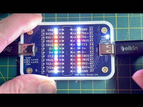
The above video covers versions 1 and 2. The current version is 3.
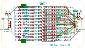
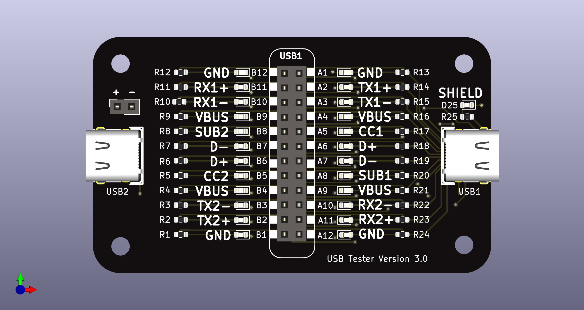
The BOM is pretty straight forward, 100 ohm resistors and whatever color LEDs you would like to use.
The USB sockets are these ones: https://www.lcsc.com/product-detail/USB%20Connectors_XUNPU-TYPEC-324-BCP24_C2835314.html
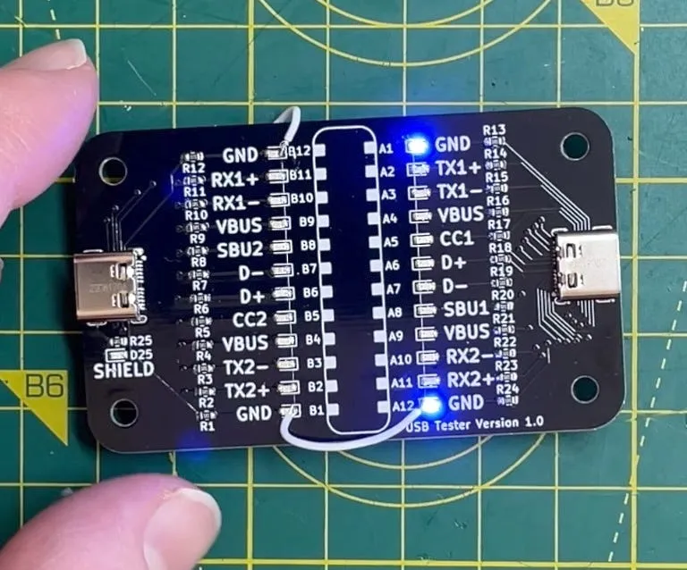
For the first version I used these USB sockets.
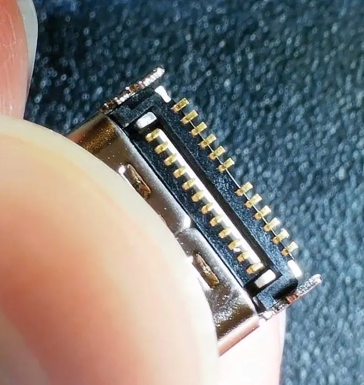
These break out all the pins - but unfortunately half the pins are hidden under the socket so you can’t see if you have solder bridges or bad connections. That coupled with a couple of design errors made the first version of the board a bit of a failure.
So for version 2 I opted to use these sockets:
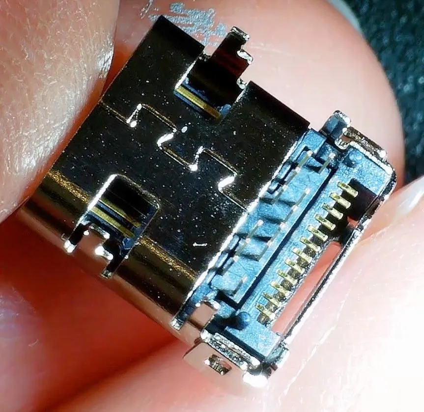
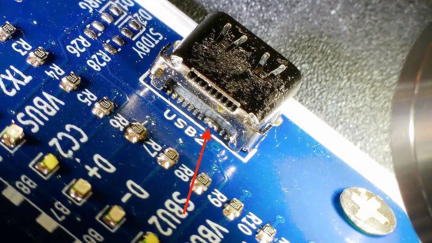
These are a lot easier to inspect. Half the pins a through hole and the other half are visible at the back of the socket.
It is still pretty hard to solder up and not get any bridges, but at least now we can see them easily.
Version 2 works pretty well, we can test various cables - for example here’s a good quality cable that should be able to for 40Gbps.
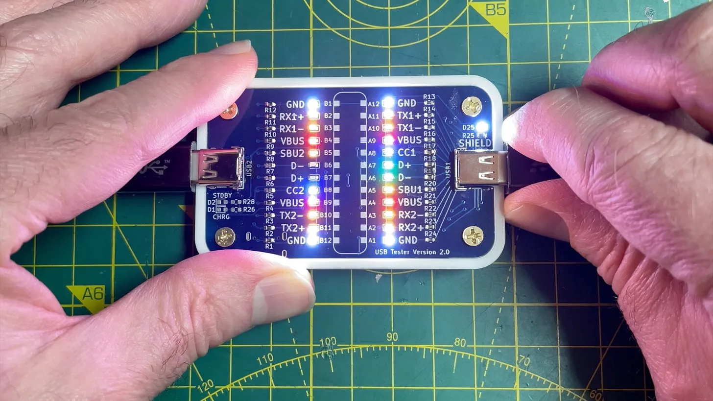
And here’s a cable that is ok for normal USB - but it’s not going to set the world on fire when it comes to speed.
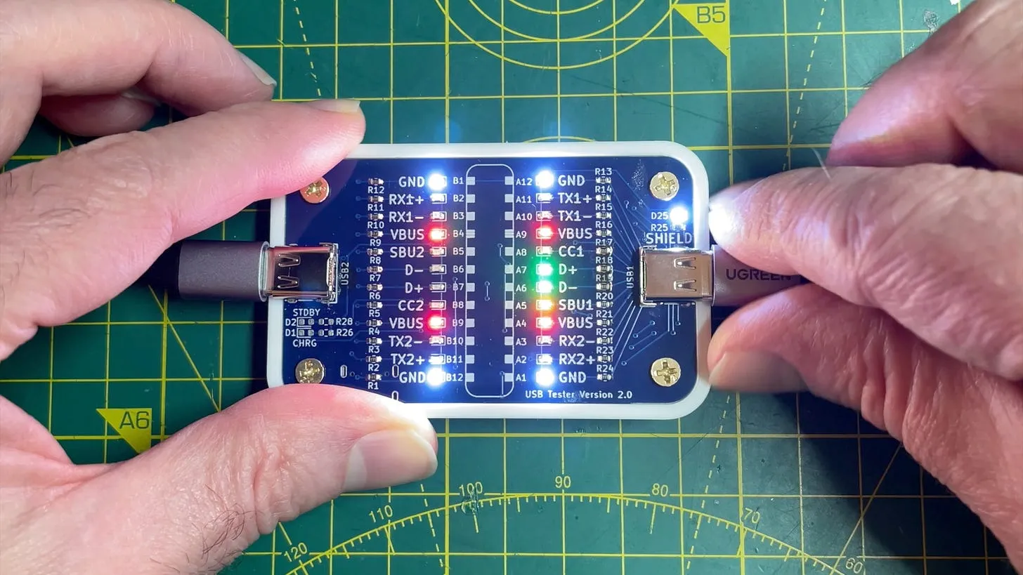
I’ve got a new version under construction. With the previous two versions it’s been really hard to tell if the sockets are soldered on properly. So I’ve now broken out all the connections and can easily build a test jig to check for shorts.
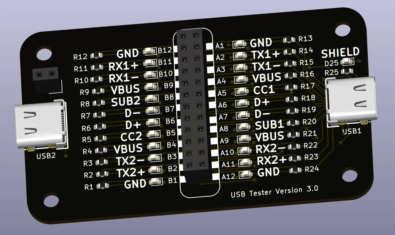
| Qty | Value | Footprint | References |
|---|---|---|---|
| 24 | 100 | Resistor_SMD:R_0603_1608Metric | R1, R2, R10, R11, R12, R13, R14, R15, R16, R17, R18, R19, R20, R21, R22, R23 +8 |
| 8 | LEDY | LED_SMD:LED_0603_1608Metric | A2, A3, A10, A11, B2, B3, B10, B11 |
| 4 | LEDG | LED_SMD:LED_0603_1608Metric | A6, A7, B6, B7 |
| 4 | LEDR | LED_SMD:LED_0603_1608Metric | A4, A9, B4, B9 |
| 4 | LEDW | LED_SMD:LED_0603_1608Metric | A1, A12, B1, B12 |
| 4 | MountingHole | MountingHole:MountingHole_3.2mm_M3 | H1, H2, H3, H4 |
| 2 | LEDB | LED_SMD:LED_0603_1608Metric | A5, B5 |
| 2 | LEDV | LED_SMD:LED_0603_1608Metric | A8, B8 |
| 2 | TYPEC-324-BCP24 | easyeda2kicad:USB-C-SMD_TYPEC-324-BCP24 | USB1, USB2 |
| 1 | 1000 | Resistor_SMD:R_0603_1608Metric | R25 |
| 1 | BS-06-B4AK008 | BAT-SMD_BS-06-B4AA012:BAT-SMD_BS-06-B4AA012 | BT2 |
| 1 | Conn_01x02 | Connector_PinSocket_2.54mm:PinSocket_1x02_P2.54mm_Vertical | J2 |
| 1 | Conn_02x12_Odd_Even | Connector_PinSocket_2.54mm:PinSocket_2x12_P2.54mm_Vertical | J1 |
| 1 | LED | LED_SMD:LED_0603_1608Metric | D25 |
It measures 69.1 × 41 mm and has 2 copper layers, 1.6 mm thick.
59 parts, built around the TYPEC-324-BCP24 and BS-06-B4AK008. The full list of its parts is on this page, with links to each part's symbol and footprint where PCBKit's library has them.
From the atomic14/usb-tester repository on GitHub, at the commit this page was made from: the board is USB-tester.kicad_pcb and its schematic USB-tester.kicad_sch. PCBKit opens the board in the browser, with nothing to install.
Its repository publishes it under the MIT licence: you may reuse it on that licence's terms (keep the author's notice, and for a copyleft licence share your changes alike).
Cath272/USB-3.1-to-SATA-6Gbps
USB 3.1(10Gbps, SuperSpeed 10Gbps, USB 3.2 gen 2) to SATA 6Gbps

davidphilipbarr/Sweep
Sweep - a small promicro based keyboard inspired by the Ferris.


VoronDesign/Voron-Hardware
Cool Hardware designed by the Voron Design group


dmcke5/NucDeck
The Open Source DIY Handheld Gaming PC!

jackw01/scanlight
A better light source for scanning color negative film

ChrisChrisLoLo/beyblock20
The magnetic, modular, 20-key macropad that can join together to form an ortholinear board