

2 layers35.6 × 88.9 mm

 atait/DIPcap
Variable capacitor based on DIP switches ranging from 1nF to 1mF
Switch boxes panelized is an open-source printed circuit board by atait, from the atait/DIPcap repository on GitHub. It is a 2-layer board of 202.2 × 229.8 mm with 881 parts on 256 nets, routed with 1,064 tracks and 96 vias.
It is built around the SMXS-08K-TP. Its parts include 216 capacitors, 32 connectors, 32 switches and 8 resistors.
A variable capacitor bank built from DIP switches. Six decades of coverage (1 nF to 1 mF) for under $10 to build.
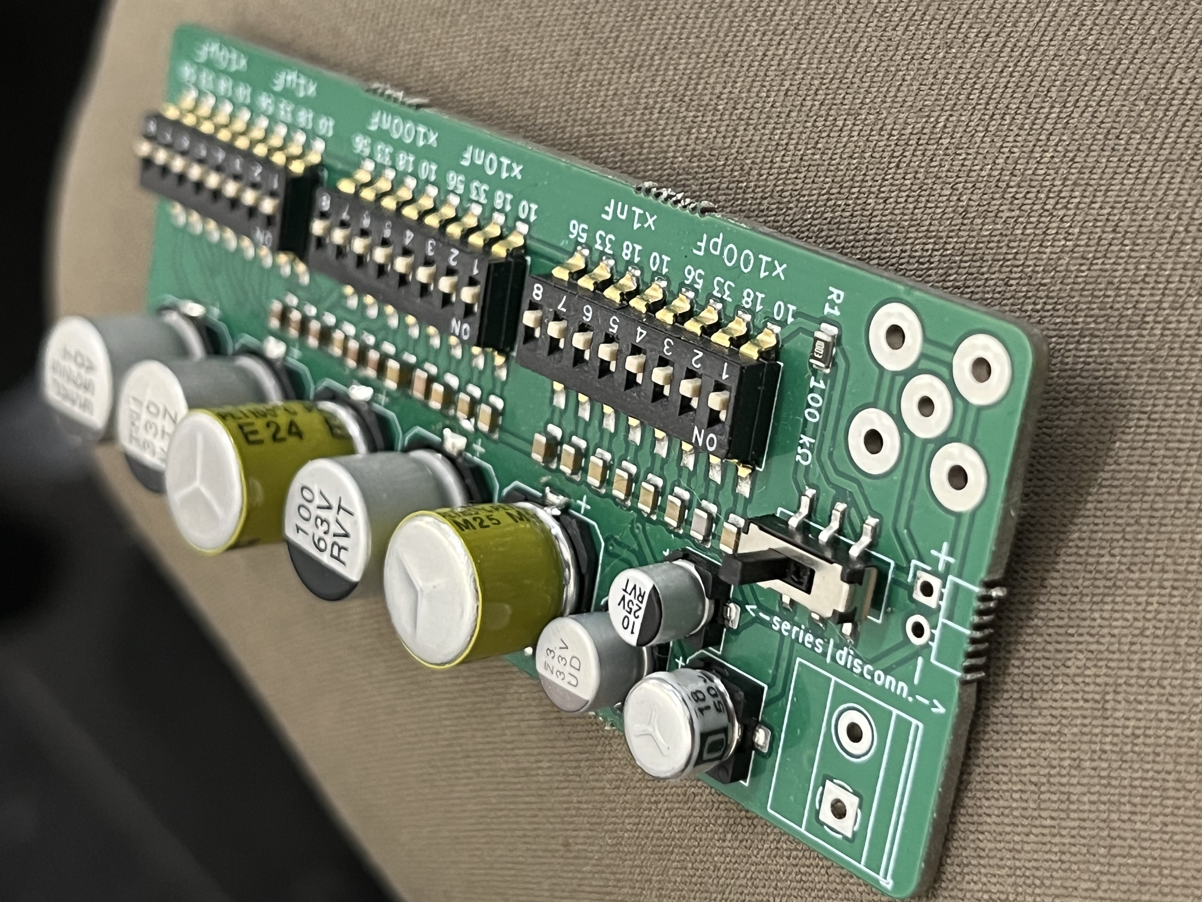
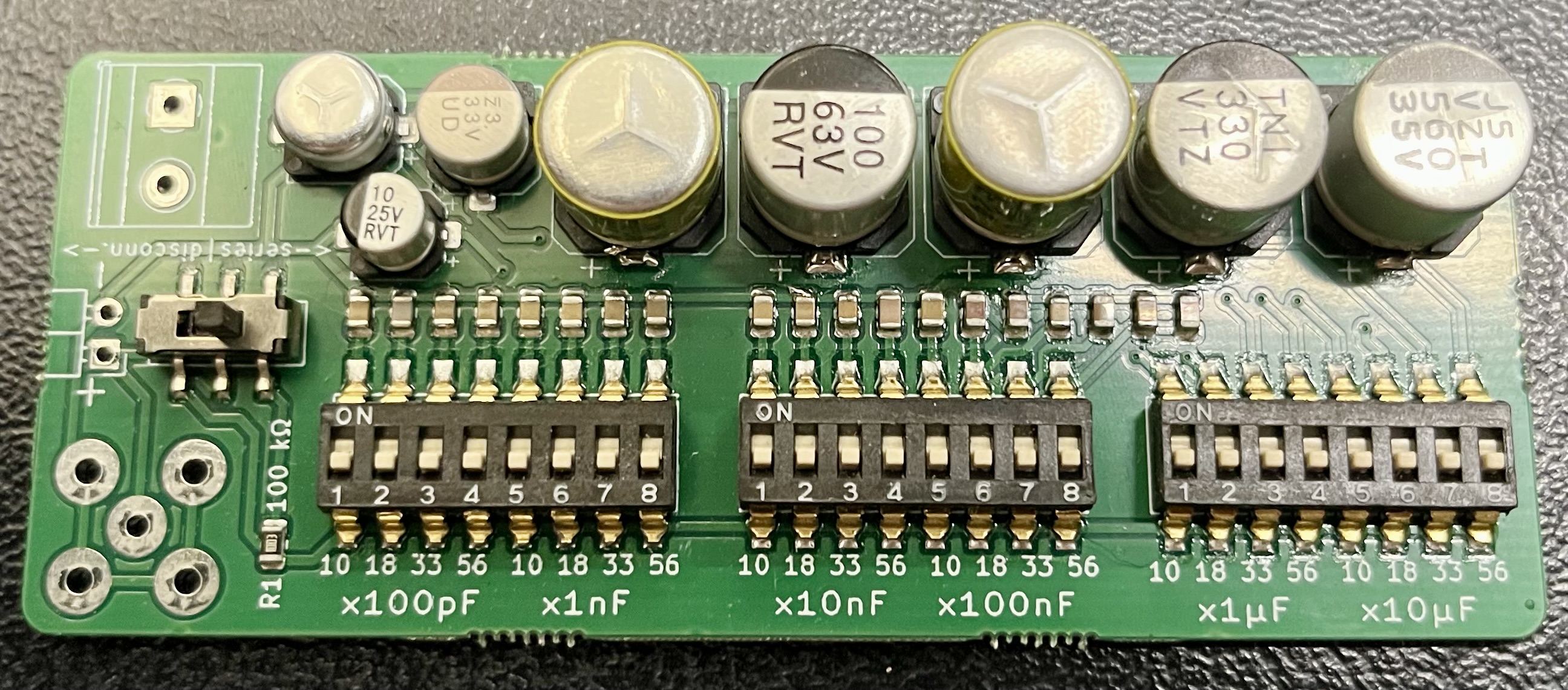
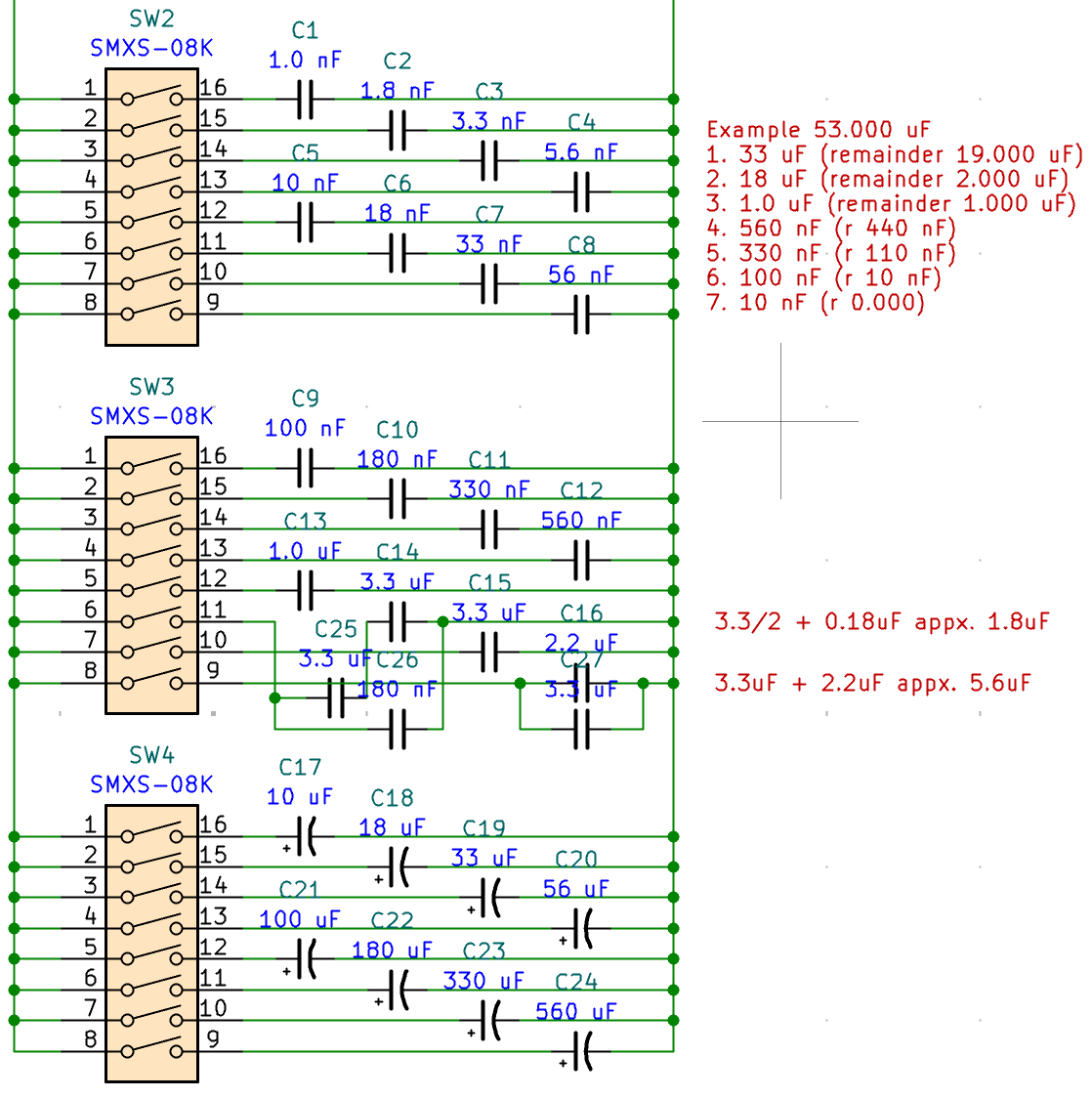
DIPcap covers six decades with 24 switches arranged in three groups of eight, using a non-standard but deliberate value series that guarantees full range coverage with the optimal number of switches per decade.
The calibration guarantee is the interesting part: even with ±10% tolerance on individual capacitors, some combination of switches will converge on any target value.
| Parameter | Value |
|---|---|
| Range | 1 nF – 1,130 µF |
| Max voltage | 0-35V, or ±50V for values < 1 µF |
| Tolerance (dead reckoning) | ±10% |
| Parasitic capacitance (all off) | 28 pF (measured) |
| Output connector | BNC + screw terminal + pin header |
| Cost to build | ~$10/unit (panelized at 8) |
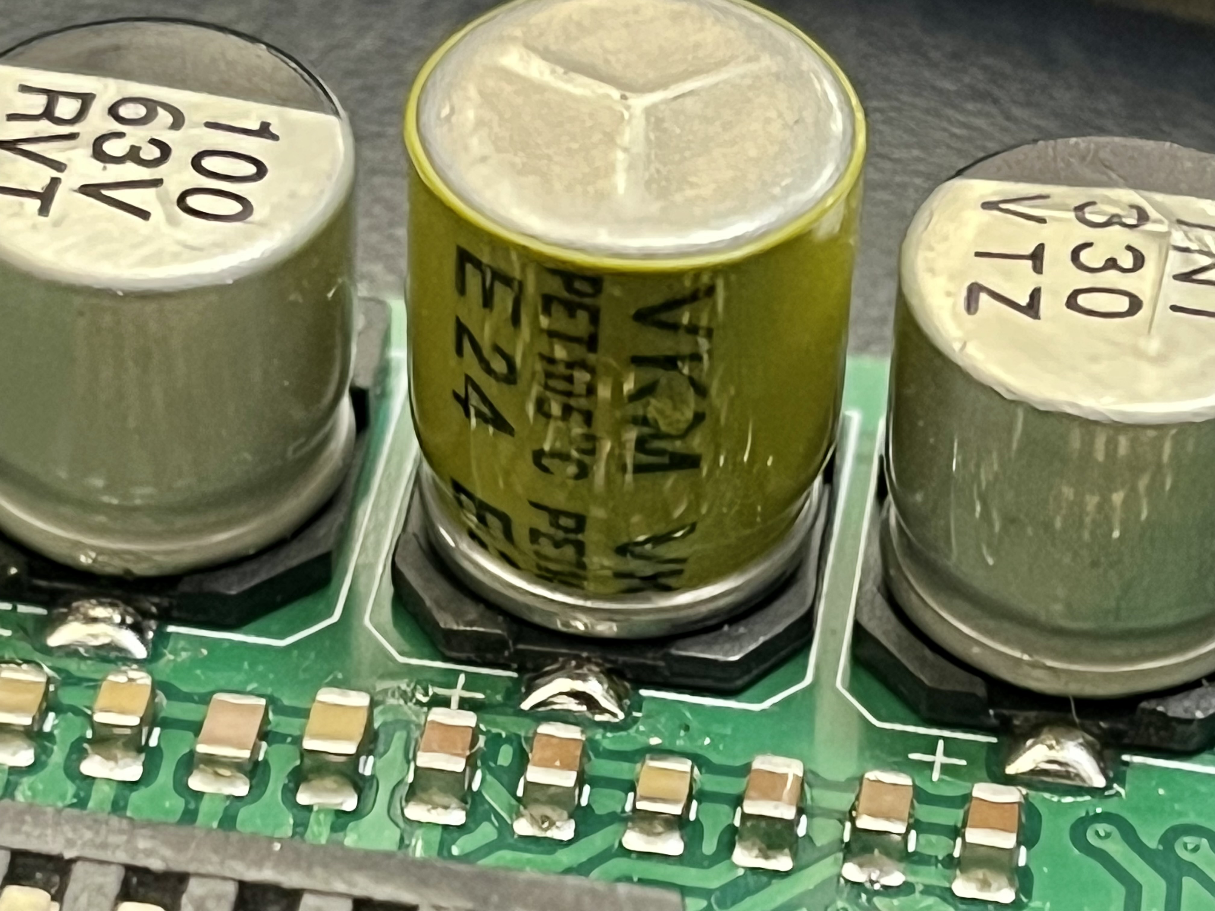
The values per decade are 10, 18, 33, 56 (in units of the decade's base, e.g. ×100pF, ×1nF, etc.). This is not a standard E-series but is drawn from E12 so that common components are available.
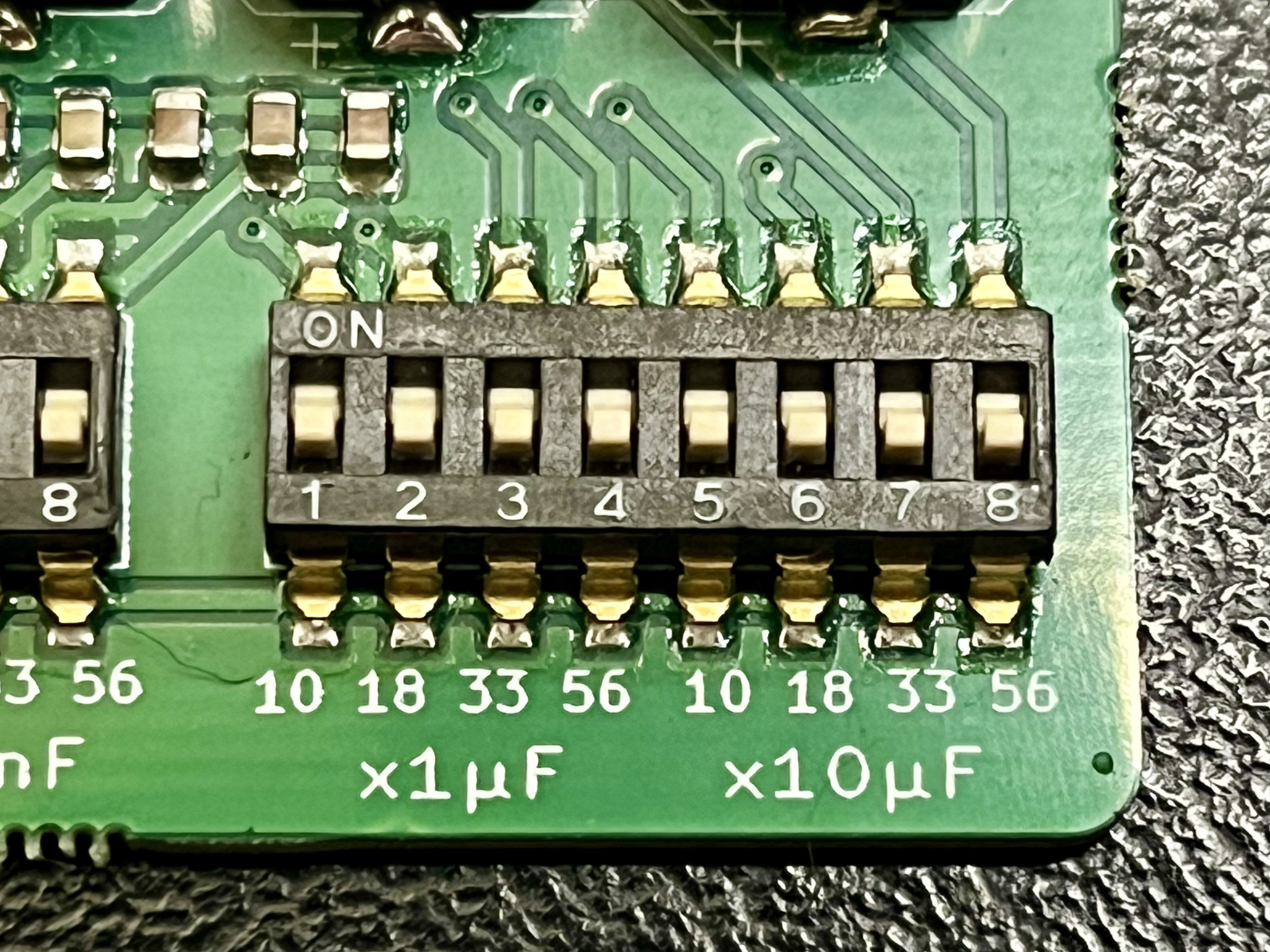
Full coverage means every value between 10–100 (in normalized units) is reachable within ±10% by some switch combination, and the next lower decade handles the remaining gap.
The choice of four switches per decade follows from a coverage argument:
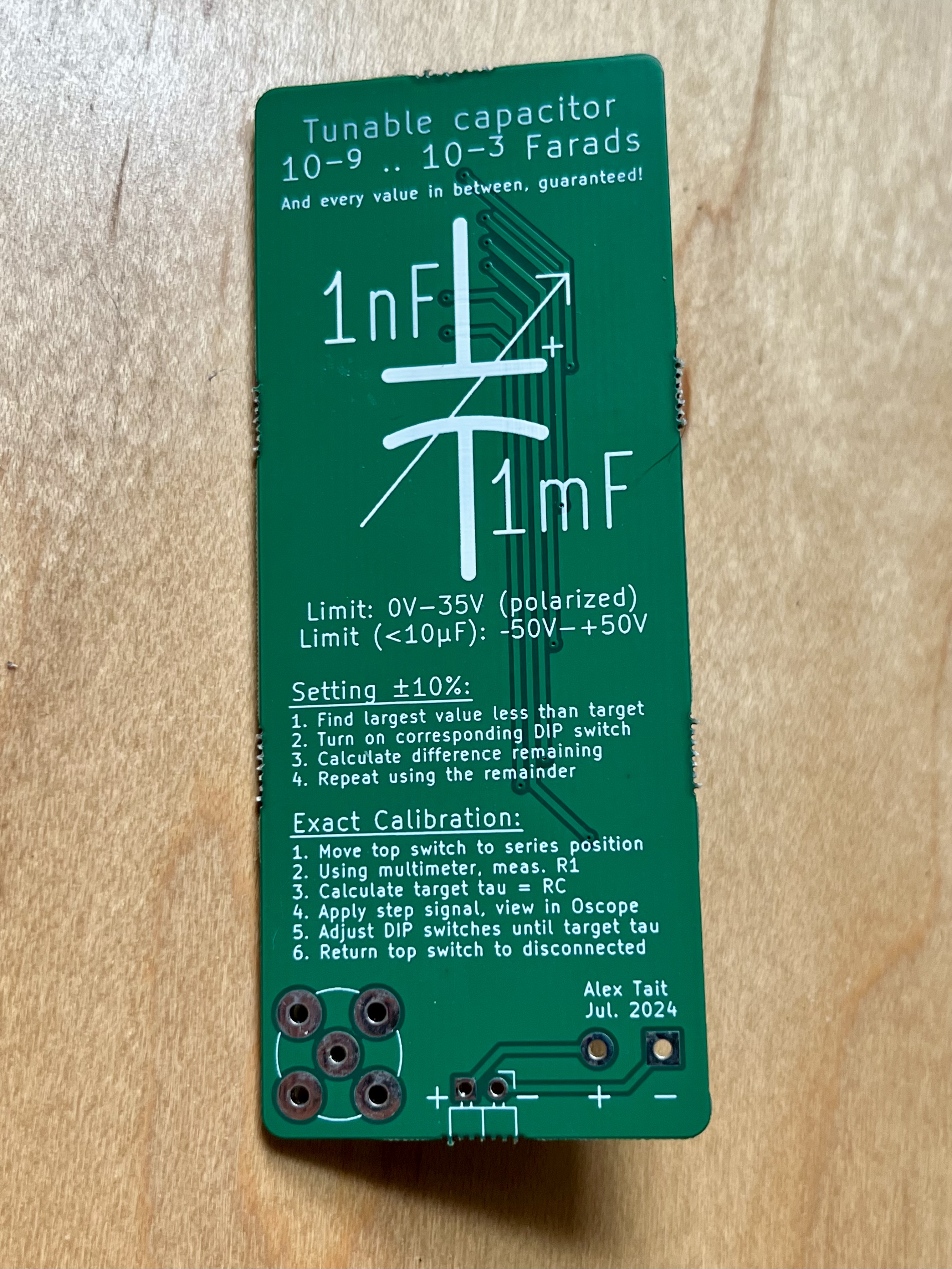
There are two ways to use DIPcap:
The instructions are silkscreened on the back of the board.
DIPresi — the same concept applied to resistance. Binary-weighted resistor bank with DIP switches, covering several decades of resistance.
Hardware released under CERN-OHL-S v2. Design files are the Complete Source as defined by the licence.
© 2026 Alex Tait — source location: https://github.com/atait/dipcap
| Qty | Value | Footprint | References |
|---|---|---|---|
| 587 | NPTH | NPTH | KiKit_MB_10_1, KiKit_MB_10_2, KiKit_MB_10_3, KiKit_MB_10_4, KiKit_MB_10_5, KiKit_MB_10_6, KiKit_MB_10_7, KiKit_MB_10_8, KiKit_MB_11_1, KiKit_MB_11_2, KiKit_MB_11_3, KiKit_MB_11_4, KiKit_MB_11_5, KiKit_MB_11_6, KiKit_MB_11_7, KiKit_MB_11_8 +571 |
| 32 | 3.3 uF | Capacitor_SMD:C_0805_2012Metric | C14, C14, C14, C14, C14, C14, C14, C14, C15, C15, C15, C15, C15, C15, C15, C15 +16 |
| 24 | SMXS-08K | atait-sensors:SW_DIP_SPSTx08_P2.54mm_easyEDA | SW2, SW2, SW2, SW2, SW2, SW2, SW2, SW2, SW3, SW3, SW3, SW3, SW3, SW3, SW3, SW3 +8 |
| 16 | 180 nF | Capacitor_SMD:C_0805_2012Metric | C10, C10, C10, C10, C10, C10, C10, C10, C26, C26, C26, C26, C26, C26, C26, C26 |
| 16 | Conn_01x02 | Connector_PinHeader_2.54mm:PinHeader_1x02_P2.54mm_Horizontal | J1, J1, J1, J1, J1, J1, J1, J1, J3, J3, J3, J3, J3, J3, J3, J3 |
| 8 | 1.0 nF | Capacitor_SMD:C_0805_2012Metric | C1, C1, C1, C1, C1, C1, C1, C1 |
| 8 | 1.0 uF | Capacitor_SMD:C_0805_2012Metric | C13, C13, C13, C13, C13, C13, C13, C13 |
| 8 | 1.8 nF | Capacitor_SMD:C_0805_2012Metric | C2, C2, C2, C2, C2, C2, C2, C2 |
| 8 | 10 nF | Capacitor_SMD:C_0805_2012Metric | C5, C5, C5, C5, C5, C5, C5, C5 |
| 8 | 10 uF | Capacitor_SMD:CP_Elec_5x5.4 | C17, C17, C17, C17, C17, C17, C17, C17 |
| 8 | 100 kΩ | Resistor_SMD:R_0805_2012Metric | R1, R1, R1, R1, R1, R1, R1, R1 |
| 8 | 100 nF | Capacitor_SMD:C_0805_2012Metric | C9, C9, C9, C9, C9, C9, C9, C9 |
| 8 | 100 uF | Capacitor_SMD:CP_Elec_10x10.5 | C21, C21, C21, C21, C21, C21, C21, C21 |
| 8 | 18 nF | Capacitor_SMD:C_0805_2012Metric | C6, C6, C6, C6, C6, C6, C6, C6 |
| 8 | 18 uF | Capacitor_SMD:CP_Elec_6.3x5.7 | C18, C18, C18, C18, C18, C18, C18, C18 |
| 8 | 180 uF | Capacitor_SMD:CP_Elec_10x12.5 | C22, C22, C22, C22, C22, C22, C22, C22 |
| 8 | 2.2 uF | Capacitor_SMD:C_0805_2012Metric | C16, C16, C16, C16, C16, C16, C16, C16 |
| 8 | 3.3 nF | Capacitor_SMD:C_0805_2012Metric | C3, C3, C3, C3, C3, C3, C3, C3 |
| 8 | 33 nF | Capacitor_SMD:C_0805_2012Metric | C7, C7, C7, C7, C7, C7, C7, C7 |
| 8 | 33 uF | Capacitor_SMD:CP_Elec_6.3x5.8 | C19, C19, C19, C19, C19, C19, C19, C19 |
| 8 | 330 nF | Capacitor_SMD:C_0805_2012Metric | C11, C11, C11, C11, C11, C11, C11, C11 |
| 8 | 330 uF | Capacitor_SMD:CP_Elec_10x10.5 | C23, C23, C23, C23, C23, C23, C23, C23 |
| 8 | 5.6 nF | Capacitor_SMD:C_0805_2012Metric | C4, C4, C4, C4, C4, C4, C4, C4 |
| 8 | 56 nF | Capacitor_SMD:C_0805_2012Metric | C8, C8, C8, C8, C8, C8, C8, C8 |
| 8 | 56 uF | Capacitor_SMD:CP_Elec_10x10 | C20, C20, C20, C20, C20, C20, C20, C20 |
| 8 | 560 nF | Capacitor_SMD:C_0805_2012Metric | C12, C12, C12, C12, C12, C12, C12, C12 |
| 8 | 560 uF | Capacitor_SMD:CP_Elec_10x10 | C24, C24, C24, C24, C24, C24, C24, C24 |
| 8 | BNC | Connector_Coaxial:BNC_TEConnectivity_1478204_Vertical | J2, J2, J2, J2, J2, J2, J2, J2 |
| 8 | Conn_01x02 | TerminalBlock_Phoenix:TerminalBlock_Phoenix_MKDS-1,5-2-5.08_1x02_P5.08mm_Horizontal | J4, J4, J4, J4, J4, J4, J4, J4 |
| 8 | SW_Push_DPDT | atait-sensors:SW_DPDT_XKB_SS-3235S-L3 | SW1, SW1, SW1, SW1, SW1, SW1, SW1, SW1 |
| 6 | Fiducial | Fiducial | KiKit_FID_B_1, KiKit_FID_B_2, KiKit_FID_B_3, KiKit_FID_T_1, KiKit_FID_T_2, KiKit_FID_T_3 |
It measures 202.2 × 229.8 mm and has 2 copper layers, 1.6 mm thick.
881 parts, built around the SMXS-08K-TP. The full list of its parts is on this page, with links to each part's symbol and footprint where PCBKit's library has them.
From the atait/DIPcap repository on GitHub, at the commit this page was made from: the board is dipcap-src/Panelized/Switch-boxes-panelized.kicad_pcb and its schematic dipcap-src/Switch-boxes.kicad_sch. PCBKit opens the board in the browser, with nothing to install.
Its repository states no licence, so its author keeps all rights: ask atait before reusing the design.


pozsarzs/zacchaeus
8-bit microcomputer built from commercially available and home-built components


SolderedElectronics/Soldered-Inkplate-6-FLICK-hardware-design
Hardware design, BOM, gerbers and 3D files for Soldered-Inkplate-6-FLICK designed by Soldered Electronics.


sparkfun/SparkFun_BlueSMiRF-v2
Documentation, firmware, and hardware Files for the SparkFun BlueSMiRF v2. These boards work as a wireless UART pipe and are a great wireless replacement for serial cables.