


2 layers89.2 × 63.5 mm
HF PA v10
kholia/HF-PA-v10
HF-PA-v10 ;) Is this the end of the search for a 5W Digital PA? HF-PA-v10 is now a rugged 10W PA! We also do 100W+ now ;)
59 parts24
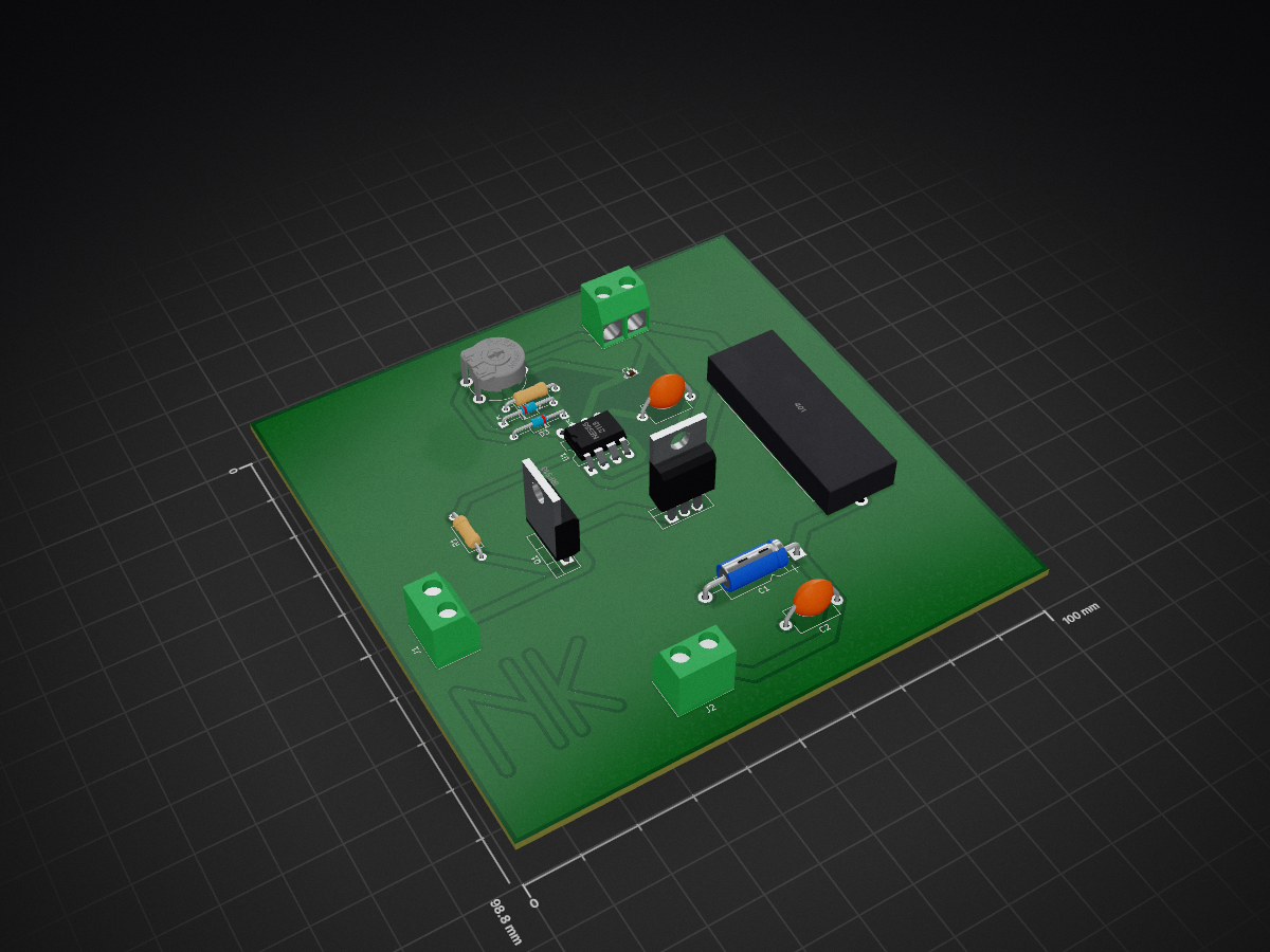
kicad, back schematic
Back is an open-source printed circuit board by Asiderr, from the Asiderr/prototype repository on GitHub. It is a 2-layer board of 100 × 98.8 mm with 16 parts on 12 nets, routed with 99 tracks and 0 vias.
It is built around the NE555 and IRF510. Its parts include 4 capacitors, 3 diodes, 3 connectors, 2 resistors and 1 IC.
| Qty | Value | Footprint | References |
|---|---|---|---|
| 3 | Screw_Terminal_01x02 | TerminalBlock:TerminalBlock_bornier-2_P5.08mm | J1, J2, J3 |
| 2 | 100n | Capacitor_THT:C_Disc_D7.5mm_W5.0mm_P10.00mm | C2, C3 |
| 2 | D | Diode_THT:D_DO-34_SOD68_P10.16mm_Horizontal | D2, D3 |
| 1 | 1k | Resistor_THT:R_Axial_DIN0207_L6.3mm_D2.5mm_P10.16mm_Horizontal | R2 |
| 1 | 22u | Capacitor_THT:CP_Axial_L11.0mm_D5.0mm_P18.00mm_Horizontal | C1 |
| 1 | 330 | Resistor_THT:R_Axial_DIN0207_L6.3mm_D2.5mm_P10.16mm_Horizontal | R1 |
| 1 | 400u | Footprints:ind_W60mm_D19mm_P38mm | L1 |
| 1 | 820p | Capacitor_SMD:C_0603_1608Metric_Pad1.05x0.95mm_HandSolder | C4 |
| 1 | D_x2_KCom_KAA | Package_TO_SOT_THT:TO-220-3_Vertical | D1 |
| 1 | IRF510 | Package_TO_SOT_THT:TO-220-3_Vertical | Q1 |
| 1 | NE555 | Package_DIP:DIP-8_W10.16mm_LongPads | U1 |
| 1 | R_POT_TRIM | Potentiometer_THT:Potentiometer_Piher_PT-10-V10_Vertical | RV1 |
It measures 100 × 98.8 mm and has 2 copper layers, 1.6 mm thick.
16 parts, built around the NE555 and IRF510. The full list of its parts is on this page, with links to each part's symbol and footprint where PCBKit's library has them.
From the Asiderr/prototype repository on GitHub, at the commit this page was made from: the board is back/back.kicad_pcb. PCBKit opens the board in the browser, with nothing to install.
Its repository states no licence, so its author keeps all rights: ask Asiderr before reusing the design.
kholia/HF-PA-v10
HF-PA-v10 ;) Is this the end of the search for a 5W Digital PA? HF-PA-v10 is now a rugged 10W PA! We also do 100W+ now ;)

kholia/Easy-Beacons-STEM
Easy-Beacons project adapted for STEM education. Powered by Raspberry Pi Pico (W) boards. WSPR + FT8 beacons for science (TM).

kholia/HF-PA-v6
RF "Lego" blocks. Quite-Linear HF broadband RF amplifier experiments for higher bands.


kholia/Global-Communications-Transceiver
Open-source files for Global Communications Transceiver


