DIY FOC Motor Controller V1: Custom Hardware & Firmware from Scratch


A custom-designed, 60V 50A Field Oriented Control (FOC) BLDC motor controller built from scratch. Designed for high-performance robotics, featuring a 4-layer power PCB, isolated USB telemetry, and CAN bus communication.
Overview
I started this project to deeply understand the hardware architecture of modern, high-power motor drivers like the VESC and ODrive. Instead of just buying an off-the-shelf driver, I wanted to design one from the ground up to learn the intricacies of power electronics, mixed-signal PCB layout, gate driving, and hardware debugging.
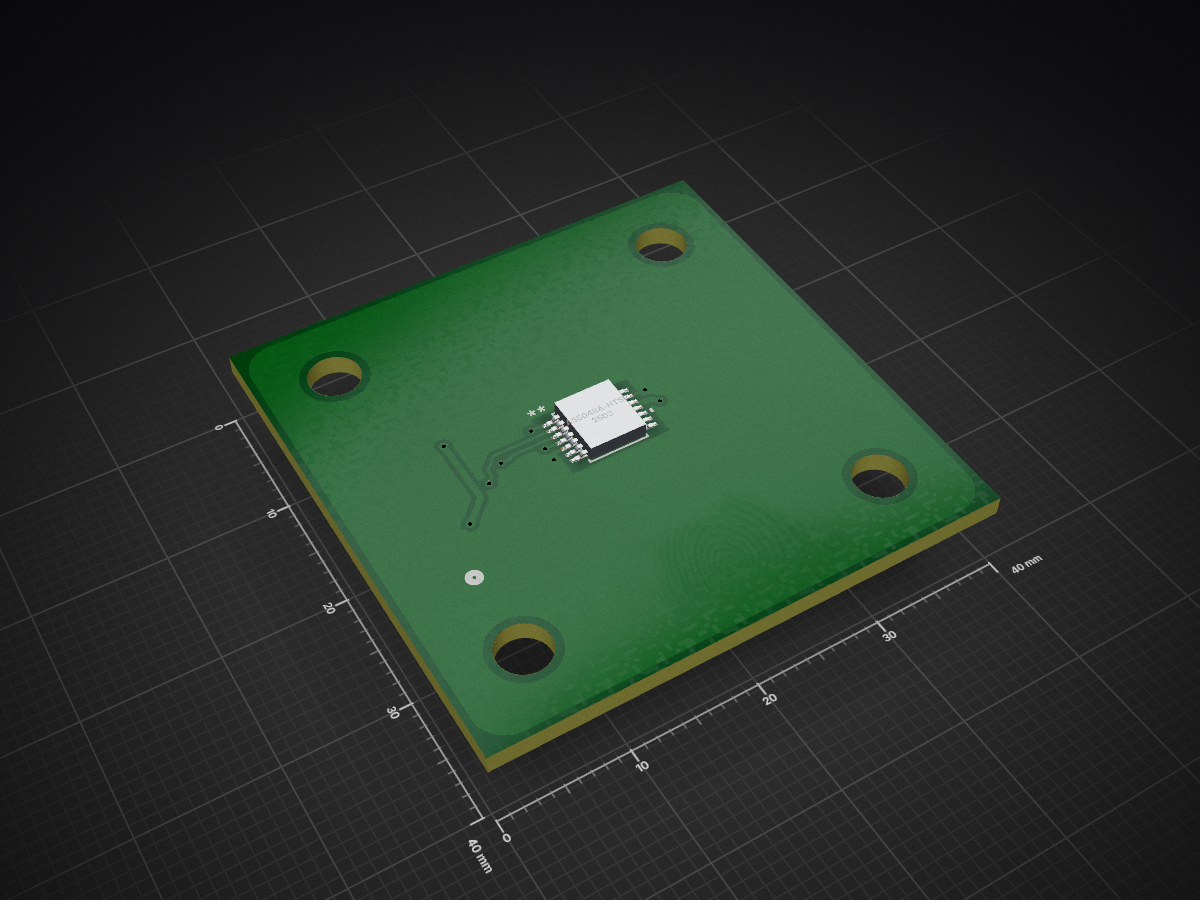
The system is split into a 4-layer main power board (handling the MCU and 60V power stage) and a separate 2-layer magnetic encoder board mounted directly to the motor. This approach kept the overall footprint compact and reduced manufacturing costs.
As the project progressed, it evolved beyond "build a VESC clone" into writing a full custom bare-metal FOC firmware stack from scratch. As of October 3, 2026, the board successfully runs closed-loop Field-Oriented Control, achieving smooth velocity control. Having fulfilled its purpose as a deep-dive educational tool into power electronics and motor control theory, this project is now officially concluded. The repository remains as a documented post-mortem and reference for DIY FOC development.
Key Features
- Working Closed-Loop FOC: Fully custom bare-metal firmware achieves smooth closed-loop current control and velocity control.
- 60V Power Stage: 60V-rated MOSFETs capable of handling 10S Li-Po battery voltages and regenerative braking spikes.
- Precision Current Sensing: 1mΩ shunt resistors utilizing strict Kelvin connections and RC-filtered differential amplifiers.
- Isolated Telemetry: ADuM3160-based USB isolation to protect the host computer from catastrophic 60V transients during live tuning.
- Robust Communication: TJA1051T/3 CAN bus transceiver with 120Ω termination for robot networking.
- Modular Encoder: Separate 2-layer AS5048A magnetic encoder PCB using JST-GH SMD connectors.
Hardware
Computing & Control
- Microcontroller: STM32F405RGT6 (Chosen for its floating-point unit, advanced motor control timers, and native VESC compatibility)
- Gate Driver: TI DRV8301 (Features a built-in 5V buck converter and dual current shunt amplifiers. Chosen over the DRV8323 for VESC compatibility)
Power Stage
- MOSFETs: Infineon IRFS7530 in D2PAK-7 (Rated for 60V, providing ample headroom for a 10S ~40V battery and regenerative braking)
- Current Sense: Yageo PU2512FK-070R001L (1mΩ, 2W metal alloy shunts)
- Protection: Littelfuse SMCJ43A TVS Diode (Clamps dangerous voltage spikes generated by motor back-EMF during hard braking)
- Connectors: Amass XT90-S (Anti-spark) for battery input
Sensing & Telemetry
- Encoder: AMS AS5048A (14-bit absolute magnetic encoder reading a 6x2.5mm diametrically magnetized NdFeB magnet)
- Temperature: Murata 10kΩ 0603 NTC Thermistor (Placed directly adjacent to the MOSFETs to monitor power stage thermals)
- Voltage Sensing: 39kΩ / 2.2kΩ voltage divider to safely scale the 60V bus down to the STM32's 3.3V ADC range
PCB Design & Layout
The board utilizes a 4-layer stackup to safely separate high-current paths from delicate digital signals:
- Layer 1 (Top): Components, massive copper polygons for Motor Phases and 42V supply.
- Layer 2 (Inner 1): Solid GND plane (Acts as an EMI shield for the signal layer).
- Layer 3 (Inner 2): Signal routing (SPI, CAN, Gate Drive traces).
- Layer 4 (Bottom): Additional GND and 42V copper pours, heavily via-stitched to the top layer to maximize current carrying capacity and thermal dissipation.
Challenges and Lessons Learned
Building a high-power motor controller from scratch provided an intense, hands-on education in hardware and firmware debugging.
Solder Wicking and Clearance Tolerances (V1.0)
After freshly soldering the V1.0 PCB, I felt an unusually strong resistance when I tried to rotate the motor by hand. I learned this is caused by back-EMF when phase wires are shorted together. Multimeter testing confirmed that V++, GND, and all three motor phases were dead-shorted.
Upon inspection, I realized the clearance between my GND copper pour and the soldering pads for V++ and the phase wires was very small (0.15mm). When hand-soldering the massive motor wires, the liquid solder easily wicked across that tiny gap into the GND pour.
For V1.1, I redesigned the board with strict Net Classes, increasing the clearance around high-power wire pads to 0.6mm to create a physical "moat", while keeping the MCU digital clearance at 0.15mm for dense routing.
The "Bad Internet Symbol" Trap (V1.1)
After successfully assembling V1.1 with new stencils and corrected clearances, the board still exhibited a short between V++, GND, and the phase wires.
I started isolating the issue by desoldering components one by one. I checked a bare V1.0 board and found no shorts, meaning the layout itself wasn't fundamentally shorted. I desoldered the MCU and gate driver — the short was still there. Finally, I desoldered the high-side MOSFETs one by one. Removing the last high-side MOSFET finally severed the short between V++ and the motor phases.
I probed the desoldered MOSFET and found a short between Pin 7 and the Source pins (Pins 2-6). Initially, I thought the MOSFET had overheated and failed closed during hot-plate reflow. However, I looked into the Infineon datasheet and saw a catastrophic error in the third-party CAD symbol I had downloaded.
The symbol incorrectly labeled Pin 7 as "Drain". In reality, the D2PAK-7 package uses the large back EPAD as the Drain, and Pins 2 through 7 are all Source pins. Because I followed the flawed schematic, my PCB layout drew a massive copper pour that physically connected the Drain (EPAD) to the Source (Pin 7). The PCB itself was shorting the circuit by design, while the MOSFETs were actually unharmed.
Lesson learned: Never trust third-party CAD footprints without verifying against the manufacturer's datasheet.
The USB D+/D- Swap (V1.2)
With the phase-short issue resolved, V1.2 soldered up cleanly with no shorts between V++, GND, or the phase wires. After hours of VESC firmware macro configuration, I successfully flashed VESC firmware onto the board. However, the board never enumerated over USB — nothing populated on the host PC.
I re-checked the firmware configuration and it looked correct, so I moved to the hardware. It turned out to be a wiring mistake on my end, though the confusing pin naming in the schematic symbol didn't help: instead of connecting DP1↔DP2 and DN1↔DN2 (the isolator-side and MCU-side USB differential pairs), I had wired DP1↔DN1 and DP2↔DN2 — crossing the differential pairs instead of linking them straight through. I corrected this for V1.3.
The Mysterious Non-Enumerating USB (V1.3)
V1.3 fixed the DP/DN wiring mistake. USB still did not enumerate.
At this point I was confident the hardware was correct, so I wrote a minimal bare-metal STM32 firmware (via STM32CubeMX, STM32CubeIDE, and STM32CubeProgrammer) with nothing but a USB CDC "hello world" to test enumeration independently of VESC firmware. It worked immediately — the host PC detected the board and the virtual COM port came up cleanly. This confirmed the hardware (including the USB isolation and the DP/DN fix) was fine, and the problem was somewhere inside VESC firmware itself.
After a weekend of digging, my working theory is that VESC firmware assumes VBUS sensing on a specific pin by default, which on my board doesn't correspond to an actual VBUS-sensing net — that pin (PA9 / TIM1_CH2) is repurposed as a motor PWM output on my hardware. If VESC firmware is waiting on a VBUS-sense signal that physically doesn't exist on my board, USB enumeration would never complete, since the firmware assumes the connection is dead.
Rather than dig further into VESC's fairly large and unfamiliar codebase to patch around this, I decided to use this as an opportunity to learn embedded systems more deeply from first principles by writing my own bare-metal FOC firmware from scratch.
The Deceiving Cogging Torque (Open-Loop Commutation)
After first achieving open-loop commutation, I later struggled to reproduce it and assumed something had regressed in the firmware. After investigation, I realized the real cause: during my initial successful test, the motor had warmed up from repeated open-loop parameter tuning, which reduced its cogging torque (magnetic detent force) enough for the open-loop drive to overcome it smoothly. On a cold motor, the same open-loop parameters weren't enough to break through cogging torque cleanly. This was a good reminder that motor behavior is temperature-dependent, and that "it worked once" isn't the same as "it's tuned correctly."
Missing Bulk Decoupling Capacitor (Current Sensing Noise)
While debugging noisy phase current readings, a senior pointed out that the DRV8301's built-in 5V buck converter was missing a bulk decoupling capacitor on my board. Without it, switching-induced ripple on the 5V rail was likely feeding through to the gate driver's built-in current sense amplifiers, degrading signal quality. I added the missing capacitor directly onto the existing V1.3 board (Frankenstein-style, dead-bug soldered), which noticeably cleaned up the current readings enough for stable closed-loop control. This will be properly integrated into the layout for the next PCB revision.
Current Sensing Offsets and Phase Anomalies (The Final Hurdle)
While closed-loop velocity control was achieved, the final hurdle involved anomalies in the low-side current sensing. Through telemetry analysis under load, I observed three distinct issues:
- DC Offsets: Despite software calibration, i_a exhibited a heavy positive offset (min -0.05A, max 0.35A), i_b (calculated) had a heavy negative offset, and i_c was relatively balanced. This points to inherent analog front-end biases or layout-induced ground offsets.
- Noise: Low-side sensing is notoriously susceptible to switching noise. Even with ADC sampling synchronized to the timer's update event (the "quiet window"), the raw data remained spiky, pushing the limits of the software's low-pass filters.
- The 180-Degree Phase Shift Anomaly: Telemetry revealed that i_a and i_c appeared to be roughly 180 degrees out of phase, rather than the expected 120 degrees. Initially, one might suspect a flipped differential pair on the PCB, but mathematically, inverting a 120-degree signal results in a 300-degree (-60 degree) phase shift, not 180 degrees. This anomaly is much more likely an artifact of severe layout-induced noise, ground bounce, or the inherent limitations of low-side current sensing on a noisy DIY board skewing the reconstructed waveforms.
Lesson learned: Mixed-signal PCB layout for high-current switching requires extreme care. For V2, I would transition to in-line current sensing with dedicated isolated amplifiers, ensure perfectly matched differential pair routing for the shunts, and implement a more robust analog filtering stage.
Custom Firmware Development
Since abandoning VESC firmware, I built a custom bare-metal firmware stack using STM32CubeMX, STM32CubeIDE, and FreeRTOS (for telemetry and state management), with the actual FOC control loop implemented as a hardware-timer/ADC-interrupt-driven routine.
MCU Pinout
PWM (TIM1, Center-Aligned, Complementary Outputs)
| Pin | Function |
|---|
| PA8 | TIM1_CH1 |
| PA9 | TIM1_CH2 |
| PA10 | TIM1_CH3 |
| PB13 | TIM1_CH1N |
| PB14 | TIM1_CH2N |
| PB15 | TIM1_CH3N |
ADC (Current & Voltage Sensing)
| Pin | Function |
|---|
| PA0 | ADC1_IN0 — Phase A Current |
| PA1 | ADC2_IN1 — Phase C Current |
| PA2 | ADC3_IN2 — VBUS Voltage Sensing |
| PA3 | ADC3_IN3 — MOSFET Temperature |
DRV8301 Gate Driver (SPI1)
| Pin | Function |
|---|
| PC1 | EN_GATE |
| PC2 | DC_CAL |
| PC0 | nFAULT (EXTI0) |
| PB3 | SPI1_SCK |
| PB4 | SPI1_MISO |
| PB5 | SPI1_MOSI |
| PD2 | CS |
Encoder (SPI3)
| Pin | Function |
|---|
| PC10 | SPI3_SCK |
| PC11 | SPI3_MISO |
| PC12 | SPI3_MOSI |
| PA15 | CS |
CAN
| Pin | Function |
|---|
| PB8 | CAN1_RX |
| PB9 | CAN1_TX |
USB
Critical note: VBUS sensing on PA9 is intentionally not used — PA9 is a motor PWM pin on this board (see the V1.3 debugging story above). USB is forced to enumerate without relying on VBUS sensing.
STM32CubeMX Configuration Notes
- Deadtime configured on the PWM timer to prevent shoot-through.
- Center-aligned PWM mode for reduced current ripple.
- ADC sampling is hardware-synchronized to PWM switching using TIM1's "Update Event" as the ADC "Trigger Event Selection," so current is always sampled at a consistent point in the switching cycle.
- Third phase current is reconstructed using Kirchhoff's Current Law rather than measured directly (only two shunts are sensed).
- ADC current sensing uses injected conversion mode so it can be hardware-triggered directly by the timer.
- ADC interrupt enabled in NVIC settings for the current-sensing ADC.
- Encoder SPI configured with DMA in full-duplex master mode.
- USB configured using the USB CDC class for direct serial communication with the host PC.
Firmware Development Progress
- ✅ Pinout and hardware configuration in CubeMX
- ✅ USB CDC enumeration working
- ✅ DRV8301 register read helper function + gate driver wake-up sequence
- ✅ SPI encoder DMA callback
- ✅ Open-loop SPWM commutation and tuning
- ✅ DRV8301 register write helper function for current amplifier gain configuration
- ✅ ADC hardware interrupt callback for current sensing (
HAL_ADC_ConvCpltCallback)
- ✅ FOC algorithm implemented inside
HAL_ADC_ConvCpltCallback
- ✅ Closed-loop current control achieved
- ✅ Closed-loop velocity control achieved — smooth motor spin under true FOC
Current Firmware State (Final)
- Closed-loop Field-Oriented Control is working on hardware: the motor spins smoothly under closed-loop velocity control.
- Open-loop SPWM commutation, ADC-synchronized current sensing, and gate driver configuration are validated.
- Future Improvements (Left as an exercise for V2): Transitioning to in-line current sensing to resolve the noise and phase shift anomalies, implementing automatic motor R and L measurement, and adding trajectory generation (slew-rate limiting) for smoother bidirectional startups.
Current Status
- V1.0 & V1.1: Deprecated — used for footprint verification and short-circuit debugging (solder wicking clearance issue, mislabeled MOSFET footprint).
- V1.2: Deprecated — resolved the phase-short issues from V1.0/V1.1, but had a USB differential pair wiring mistake (DP/DN crossed) that prevented USB enumeration.
- V1.3 (Final): USB wiring fixed and verified via custom bare-metal USB CDC test firmware. Pivoted to a fully custom bare-metal FOC firmware stack. Closed-loop FOC achieved and validated on hardware. Smooth closed-loop velocity control is working. The project is now officially closed, serving as a successful proof-of-concept and an invaluable learning experience in embedded systems and power electronics.
Project Timeline
| Date | Milestone |
|---|
| Jun 5 | Project start |
| Jun 19 | Theory research complete |
| Jul 2 | Schematic & component sourcing complete |
| Jul 13 | V1.0 PCB layout complete |
| Jul 23 | V1.0 assembled |
| Jul 27 | V1.0 testing — discovered phase/GND short from insufficient copper clearance (0.15mm) |
| Jul 30 | V1.1 redesigned with wider clearances |
| Aug 22 | V1.1 assembled — short persisted |
| — | Root cause found: mislabeled MOSFET footprint (Drain/Source swap) |
| Aug 28 | V1.2 arrives (footprint fixed) |
| — | Discovered incorrect USB D+/D- wiring |
| Sep 9 | V1.3 arrives (USB wiring corrected) |
| Sep 13 | Began VESC firmware integration — blocked by USB enumeration failure |
| Sep 17 | Diagnosed VBUS-sensing conflict; pivoted to custom bare-metal firmware |
| Sep 19 | Open-loop commutation achieved (later traced intermittent failures to motor-temperature-dependent cogging torque) |
| Sep 22 | ADC current sensing achieved (noisy — later traced to missing decoupling capacitor) |
| Sep 24 | Fixed missing decoupling capacitor; current sensing quality improved |
| Sep 25 | Closed-loop current control achieved |
| Sep 28 | Closed-loop velocity control achieved — true FOC working |
| Oct 3 | Telemetry analysis completed. Project officially concluded and documented as a post-mortem. |